

Page 1
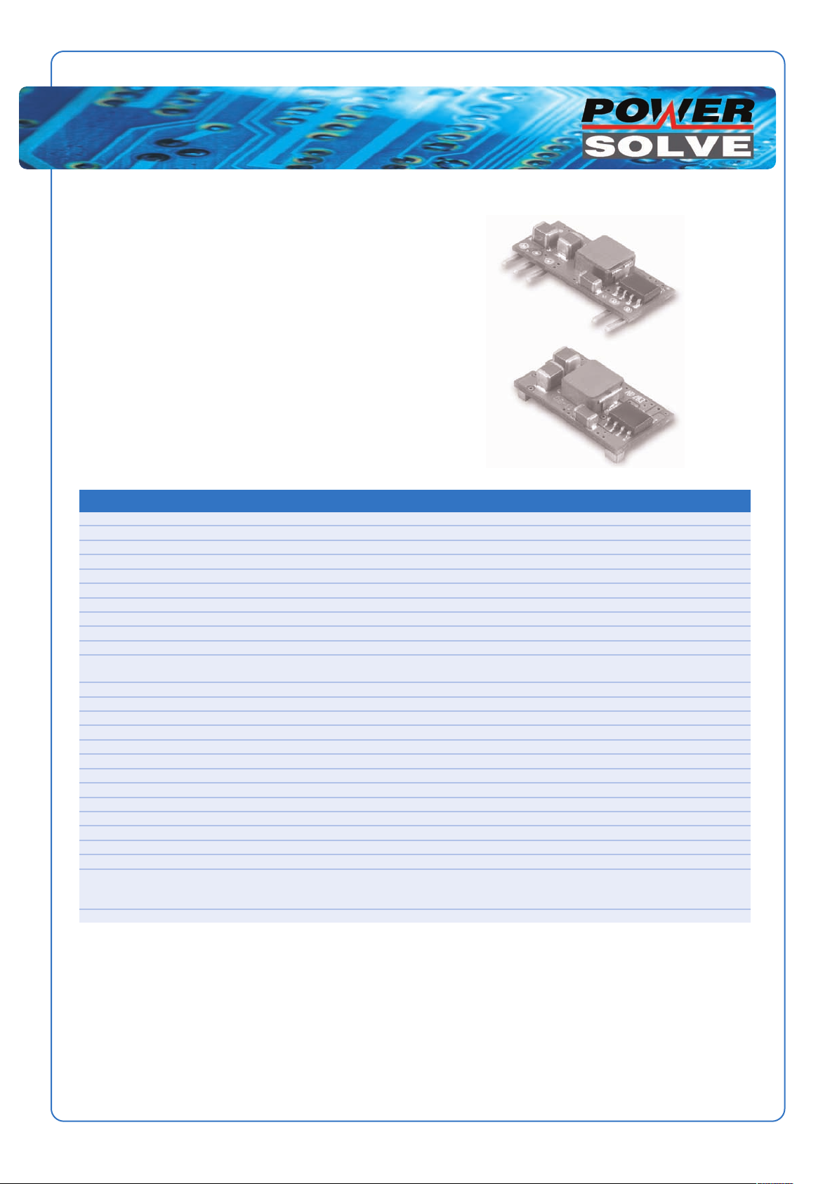
DC-DC Switching Regulator
SR05-05 Series
www.powersolve.co.uk
5A SIP & SMT Packages
Non-Isolated
Features
• Non-Isolated POL Converter
• SIP / SMT Packages
• Output Current 5A
• Input Voltage Range 3.0 - 5.5VDC
• Output Voltage Range 0.75 - 3.63VDC
• Efficiency to 94%
• Over Temperature Protection
• Continuous Short Circuit Protection
• Remote On/Off Control
Electrical Specification
INPUT
Input Voltage Range 3.0 - 5.5V (Vout set < Vin - 0.5VDC)
Under Voltage Lock-out 2.0V typ. (Power Up)
1.9V typ. (Power Down)
Input Filter Capacitive
Remote On/Off Control Open Circuit or equal to Vin (Module On)
<0.4VDC (Module Off)
OUTPUT
Voltage Accuracy ±1.5% max.
Transient Response: 25% step load change <200µ sec.
Ripple and Noise (20MHz BW) [3] 20mV rms, 50mV pk-pk max.
Temperature Coefficient ±0.03% / °C
Short Circuit Protection Continuous
Line Regulation [1] ±0.4%
Load Regulation [2] ±0.5%
Capacitive Load, Low ESR 3000µF max.
External Trim Adj. Range (see table) Vo = 0.75 - 3.63VDC
GENERAL
Efficiency See Table
Isolation Voltage Non-Isolated
Switching Frequency 300KHz typ.
Over Temperature Protection 120°C typ.
Operating Temperature Range -40°C to +85°C
Power Derating See derating curves
Storage Temperature Range -55°C to +125°C
Dimensions 22.9 x 10.16 x 5.6 mm (0.90 x 0.40 x 0.22 Inches) (SIP Package)
Case Non-potted open frame type
Weight 2.3g
NOTE:
1. Measured from High Line to Low Line (Vo set to 1.8VDC).
2. Measured from Full Load to No Load (Vo set to 3.3VDC).
3. Output noise & ripple is measured with a 10µF tantalum & 1µF ceramic capacitor across the output.
4. It is recommended to put a 100µF capacitor with ESR<100mΩ across the input to reduce the input ripple voltage.
5. Suffix ‘N’ to model number for Negative Logic Remote On/Off Control.
20.3 x 11.43 x 6.09 mm (0.80 x 0.45 x 0.24 Inches) (SMT Package)
Typical at nominal line, full load & 25°C unless otherwise stated.
Powersolve Electronics Ltd. 8A Arnhem Road, Newbury, RG14 5RU. England
Tel: 01635 521858 Fax: 01635 523771 Email: [email protected]
Page 2
DC-DC Switching Regulator
www.powersolve.co.uk
Output Voltage and Current Ratings
MODEL INPUT OUTPUT OUTPUT INPUT CURRENT % EFF.
SR05-05-33TH 3.0 - 5.5VDC 1.2V 5A 30mA 1412mA 85%
(SIP Package) 3.0 - 5.5VDC 1.5V 5A 30mA 1724mA 87%
SR05-05-33SM 3.0 - 5.5VDC 2.0V 5A 35mA 2222mA 90%
(SMT Package) 3.0 - 5.5VDC 2.5V 5A 35mA 2217mA 92%
Nominal Input Voltage 5VDC.
VOLTAGE VOLTAGE CURRENT No Load Full Load
3.0 - 5.5VDC 0.75V 5A 25mA 949mA 79%
3.0 - 5.5VDC 1.8V 5A 35mA 2022mA 89%
4.5 - 5.5VDC 3.3V 5A 35mA 3511mA 94%
External Resistor Values for
Programming Output Voltage
Vo set (V) Rtrim (KΩ)
0.75 Open
1.2 41.71
1.5 22.98
1.8 14.96
2.0 11.75
2.5 6.93
3.3 3.15
3.63 2.20
Simplified Schematic
Mechanical and Connection Details
SIP Packages
SR05-05-33SM (Vo = 3.3V) Derating CurveSR05-05-33TH (Vo = 3.3V) Derating Curve
All Dimensions in Inches (mm).
Tolerance: Inches x.xx ±0.02 x.xxx ±0.010
Millimeters x.x ±0.5 x.xx ±0.25
SMT Packages
BOTTOM VIEW OF BOARD
Pin Function
1 +Vout
2 Trim
3 Common
4 +Vin
5 On/Off
Powersolve Electronics Ltd. 8A Arnhem Road, Newbury, RG14 5RU. England
Tel: 01635 521858 Fax: 01635 523771 Email: [email protected]
 Loading...