

Power MATE TECHNOLOGY FEC15 User Manual
A
r
A
A
A
•
查询FEC15供应商
• 15 WATTS OUTPUT POWER
• 2:1 WIDE INPUT VOLTAGE RANGE
• INTERNATIONAL SAFETY STANDARD APPROVAL
• SIX-SIDED CONTINUOUS SHIELD
• HIGH EFFICIENCY UP TO 88%
VER:03 1 / 2
• STANDARD 2” X 1” X 0.4” PACKAGE
UL E193009
TUV
CB
CE MARK
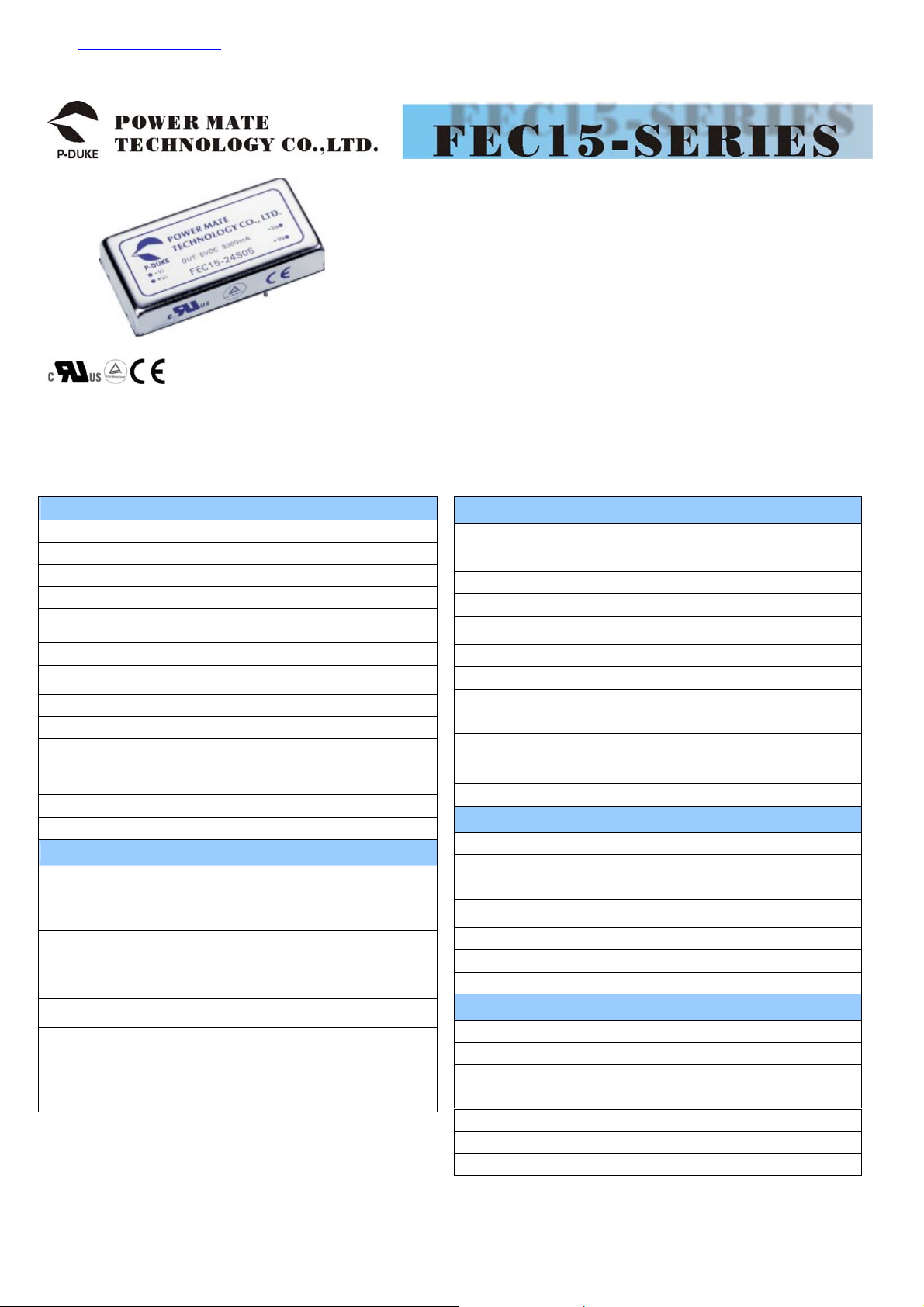
The FEC15 series offer 15 watts of output power from a 2 x 1 x 0.4 inch package. The
FEC15 series with 2:1 wide input voltage of 9-18, 18-36 and 36-75VDC. The FEC15
features 1600VDC of isolation, short-circuit and over-voltage protection, as well as six
sided shielding. A safety approval to EN60950-1 and UL60950-1. All models are
particularly suited to telecommunications, industrial, mobile telecom and test equipment
applications.
FIXED SWITCHING FREQUENCY
TECHNICAL SPECIFICATION All specifications are typical at nominal input, full load and 25ºC otherwise noted
OUTPUT SPECIFICATIONS
Output power 15 Watts max
Voltage accuracy Full load and nominal Vin ± 1%
Minimum load (Note 1)
Line regulation LL to HL at Full Load
Load regulation 10% to 100% FL
Cross regulation (Dual) Asymmetrical load 25% / 100% FL ± 5%
Ripple and noise 20MHz bandwidth
Temperature coefficient
Transient response recovery time 25% load step change 250uS
Over voltage protection
(Zener diode clamp)
Over load protection % of FL at nominal input 150% max
Short circuit protection Hiccup, automatics recovery
3.3V output
5V output
12V output
15V output
Single
Dual
Single
Dual
10% of FL
± 0.5%
± 0.5%
± 1%
50mVp-p
75mVp-p
±0.02% / ºC, max
INPUT SPECIFICATIONS
12V nominal input
Input voltage range
Input filter Pi type
Input surge voltage
100mS max
Input reflected ripple (Note 2) Nominal Vin and full load 20mAp-p
Start up time
Remote ON/OFF (Note 3)
(Positive logic)
(Negative logic)
Remote off input current
Nominal Vin and
constant resistive load
24V nominal input
48V nominal input
12V input
24V input
48V input
DC-DC ON
DC-DC OFF
DC-DC ON
DC-DC OFF
Nominal input
Power up 20mS typ
Open or 3.5V < Vr < 12V
Short or 0V < Vr < 1.2V
Short or 0V < Vr < 1.2V
Open or 3.5V < Vr < 12V
9 – 18VDC
18 – 36VDC
36 – 75VDC
36VDC
50VDC
100VDC
20mA
GENERAL SPECIFICATIONS
Efficiency See table
Isolation voltage 1600VDC, min
Isolation resistance
Isolation capacitance 300pF, max
Switching frequency
pprovals and standard IEC60950-1, UL60950-1, EN60950-1
Case material Nickel-coated coppe
Base material Non-conductive black plastic
Potting material Epoxy (UL94-V0)
3.9V
Dimensions
6.2V
Weight 27g (0.95oz)
15V
18V
MTBF (Note 4) 2.041 x 10⁶ hrs
Single output
Dual output
2.00 X 1.00 X 0.40 Inch
(50.8 X 25.4 X 10.2 mm)
ENVIRONMENTAL SPECIFICATIONS
Operating temperature range -40ºC ~ +85ºC (with derating)
Maximum case temperature 100ºC
Storage temperature range -55ºC ~ +105ºC
Thermal impedance (Note 5)
Thermal shock MIL-STD-810D
Vibration 10~55Hz, 10G, 30minutes along X,Y and Z
Relative humidity 5% to 95% RH
Nature convection
Nature convection with heat-sink
EMC CHARACTERISTICS
Conducted emissions EN55022 Class
Radiated emissions EN55022 Class A
ESD EN61000-4-2 Perf. Criteria B
Radiated immunity EN61000-4-3 Perf. Criteria
Fast transient EN61000-4-4 Perf. Criteria B
Surge EN61000-4-5 Perf. Criteria B
Conducted immunity EN61000-4-6 Perf. Criteria
9
10
ohms, min
500KHz, typ
300KHz, typ
12ºC/Watt
10ºC/Watt
(
)
V
)
)
A
A
)
Model
Number
FEC15-12S33 9 – 18 VDC 3.3 VDC 4000mA 1467mA 79 10200uF
FEC15-12S05 9 – 18 VDC 5 VDC 3000mA 1603mA 82 7050uF
FEC15-12S12 9 – 18 VDC 12 VDC 1250mA 1524mA 86 1035uF
FEC15-12S15 9 – 18 VDC 15 VDC 1000mA 1524mA 86 705uF
FEC15-12D05 9 – 18 VDC ± 5 VDC ± 1500mA 1582mA 83 ± 1020uF
FEC15-12D12 9 – 18 VDC ± 12 VDC ± 625mA 1524mA 86 ± 495uF
FEC15-12D15 9 – 18 VDC ± 15 VDC ± 500mA 1563mA 84 ± 165uF
FEC15-24S33 18 – 36 VDC 3.3 VDC 4000mA 724mA 80 10200uF
FEC15-24S05 18 – 36 VDC 5 VDC 3000mA 781mA 84 7050uF
FEC15-24S12 18 – 36 VDC 12 VDC 1250mA 772mA 85 1035uF
FEC15-24S15 18 – 36 VDC 15 VDC 1000mA 772mA 85 705uF
FEC15-24D05 18 – 36 VDC ± 5 VDC ± 1500mA 781mA 84 ± 1020uF
FEC15-24D12 18 – 36 VDC ± 12 VDC ± 625mA 762mA 86 ± 495uF
FEC15-24D15 18 – 36 VDC ± 15 VDC ± 500mA 762mA 86 ± 165uF
FEC15-48S33 36 – 75 VDC 3.3 VDC 4000mA 357mA 81 10200uF
FEC15-48S05 36 – 75 VDC 5 VDC 3000mA 396mA 83 7050uF
FEC15-48S12 36 – 75 VDC 12 VDC 1250mA 377mA 87 1035uF
FEC15-48S15 36 – 75 VDC 15 VDC 1000mA 381mA 86 705uF
FEC15-48D05 36 – 75 VDC ± 5 VDC ± 1500mA 386mA 85 ± 1020uF
FEC15-48D12 36 – 75 VDC ± 12 VDC ± 625mA 372mA 88 ± 495uF
FEC15-48D15 36 – 75 VDC ± 15 VDC ± 500mA 377mA 87 ± 165uF
Note
1. The FEC15 series required a minimum 10% loading on the output to maintain specified
regulation. Operation under no-load condition will not damage these devices, however they may
not meet all listed specification
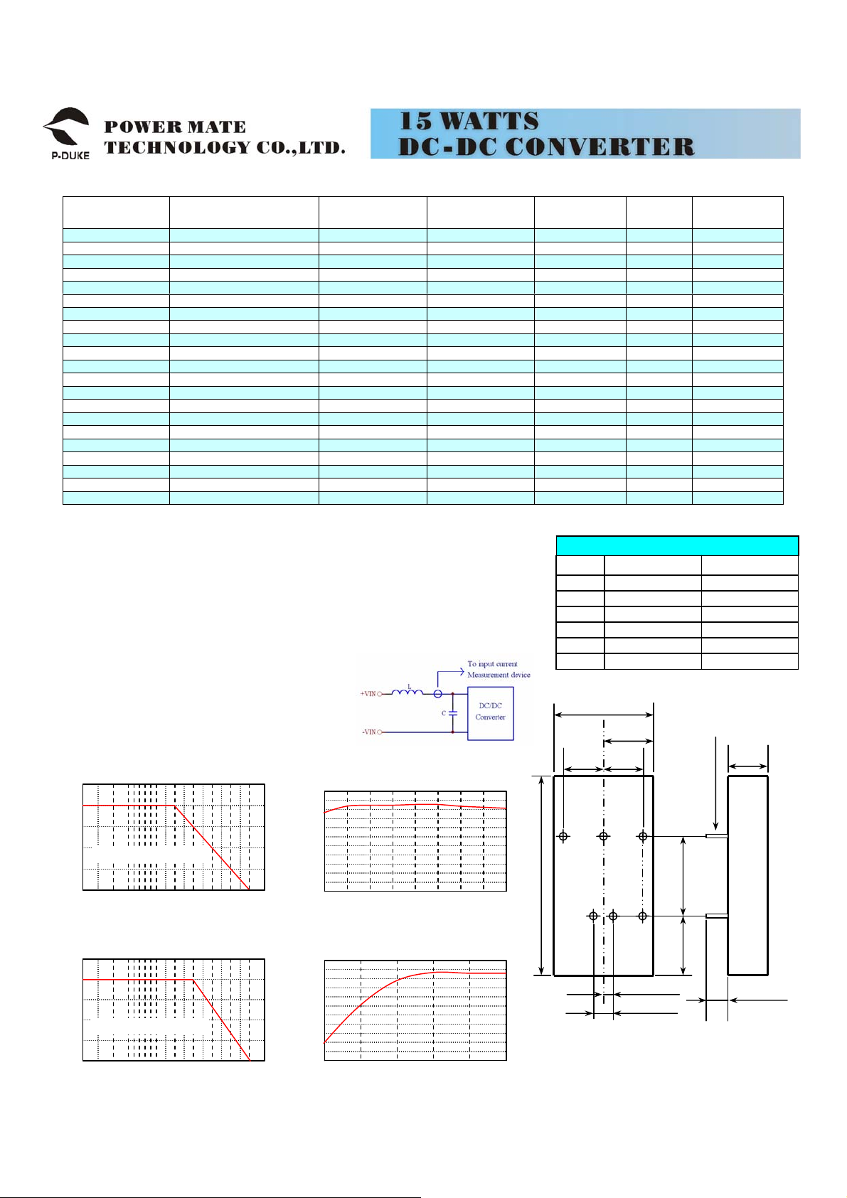
2. Please add an external filter at converter input terminals when measuring input reflected ripple,
as figure 1.
L: Simulated source impedance of 12μH C: Nippon chemi-con KMF series 100μF/100V
3. The ON/OFF control is option function. There are positive logic and negative logic. The pin
voltage is referenced to negative input
To order positive logic ON-OFF control add the suffix-P (Ex: FEC15-24S05-P)
To order negative logic ON-OFF control add the suffix-N (Ex: FEC15-24S05-N)
4. BELLCORE TR-NWT-000332. Case 1: 50% Stress,
Temperature at 40ºC. (Ground fixed and controlled
environment)
5. Heat sink is optional and P/N: 7G-0020A
6. Maximum value at nominal input voltage and full load
7. Typical value at nominal input voltage and full load
8. Test by minimum Vin and constant resistive load.
FEC15-48S05 Derating Curve
100
75
50
Nature convection
25
OUTPUT POWER (%)
0
MBIENT TEMPERATURE (ºC)
FEC15-48S05 Derating Curve
With HEAT-SINK (Note 5)
100
75
50
Nature convection
25
OUTPUT POWER (%)
0
MBIENT TEMPERA TURE (ºC
50 60 70 80 90
50 60 70 80 90
Input
Range
100-40 -25 0 -10
100-40 -25 0 -10
Output
Voltage
FEC15-48S05
Efficiency VS Input Voltage
83
82
81
80
79
78
77
76
EFFICIENCY (%)
75
74
73
83
82
81
80
79
78
77
76
EFFICIENCY (%)
70
65
50
45 55 65 7536 40
INPUTVOLTAGE(V
FEC15-48S05
Efficiency VS Output load
1.5 2 2.5
OUTPUT LOAD (A
Output
Current
Figure 1
6050 70
30.5 1
VER:03 2 / 2
(7)
Input
Current
PIN SINGLE DUAL
1 + INPUT + INPUT
2 - INPUT - INPUT
3 + OUTPUT + OUTPUT
4 NO PIN
5 - OUTPUT - OUTPUT
6 CTRL (Option) CTRL (Option)
1.00(25.4)
0.40
(10.2)
34 5
Bottom
iew
2.00(50.8)
12
1. All dimensions in Inches (mm)
Tolerance x.xx±0.02(x.x±0.5)
2. Pin Pitch tolerance ±0.014
Eff
(6)
(%)
PIN CONNECTION
0.50
(12.7)
0.40
(10.2)
6
0.10(2.5)
0.20(5.1)
0.80(20.3) 0.60(15.2)
Capacitor
Load max
COMMON
0.40
(10.2)
DIA. 0.04(1.0)
0.22(5.6)
0.35
(8)
 Loading...