

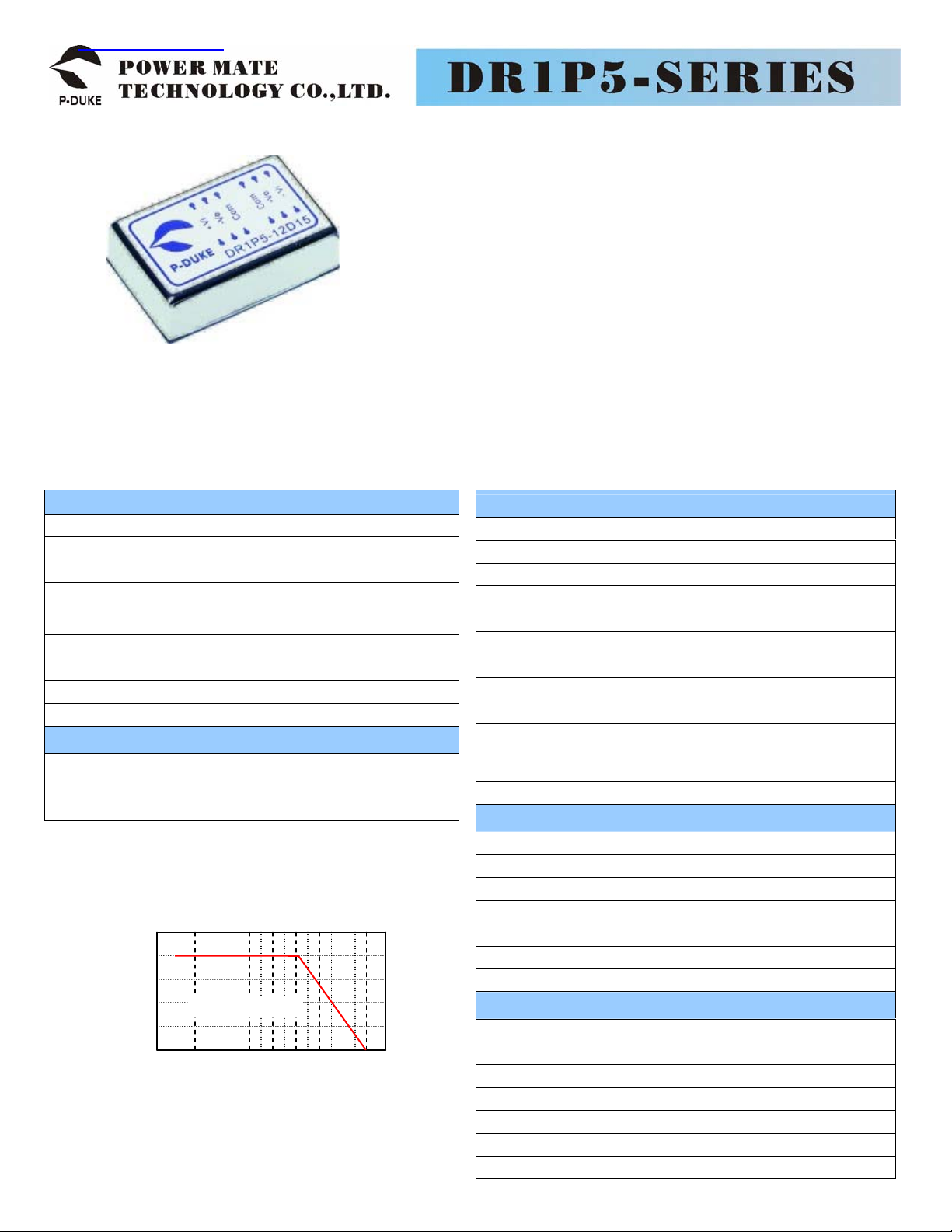
Power MATE TECHNOLOGY DRIP5 User Manual
•
r
A
查询DR1P5供应商查询DR1P5供应商
VER:03 1 / 2
• 1.5 WATTS REGULATED OUTPUT POWER
• LOW OUTPUT RIPPLE & NOISE
• PI TYPE INPUT FILTER
• 500VDC ISOLATION VOLTAGE
• HIGH EFFICIENCY UP TO 55%
• STANDARD 24 PIN DIP PACKAGE & SMD TYPE PACKAGE
FIVE-SIDED EMI SHIELD
The DR1P5 series offer 1.5 watts of output power from a package in an IC compatible 24
pin DIP configuration without derating to 71ºC ambient temperature and pin to pin
compatible to MKC03 series. DR1P5 series have input voltage of 4.5-5.5, 10.8-13.2 and
21.6-26.4VDC. DR1P5 features 500VDC of isolation voltage. A safety designed meet to
EN60950-1 and UL60950-1. All models are particularly suited to telecommunications,
industrial, mobile telecom and test equipment applications.
TECHNICAL SPECIFICATION All specifications are typical at nominal input, full load and 25ºC otherwise noted
OUTPUT SPECIFICATIONS
Output power
Voltage accuracy Full load and nominal Vin ± 4%
Minimum load 0%
Line regulation LL to HL at Full Load ± 0.3%
Load regulation 25% to 100% FL
Cross regulation Asymmetrical load 25% / 100% FL ± 5%
Ripple and noise 20MHz bandwidth 50mVp-p
Temperature coefficient
Short circuit protection Short term
D05 output
others
1.5 Watts max
± 1.5%
± 0.5%
±0.02% / ºC, max
INPUT SPECIFICATIONS
Input voltage range
Input filter Pi type
5V nominal input
12V nominal input
24V nominal input
4.5 – 5.5VDC
10.8 – 13.2VDC
21.6 – 26.4VDC
DR1P5-24S05 Derating Curve
100
75
50
25
OUTPUT POWER (%)
Nature convection
MBIENT TEMPERA TURE (ºC)
50 60 70 80 90
100 -40 0 -25 0 -10
GENERAL SPECIFICATIONS
Efficiency See table
Isolation voltage 500VDC, min
Isolation resistance
Isolation capacitance 30pF, max
Switching frequency 20KHz, min
Design meet safety standard IEC60950-1, UL60950-1,EN60950-1
Case material Nickel-coated coppe
Base material Non-conductive black plastic
Potting material Epoxy (UL94-V0)
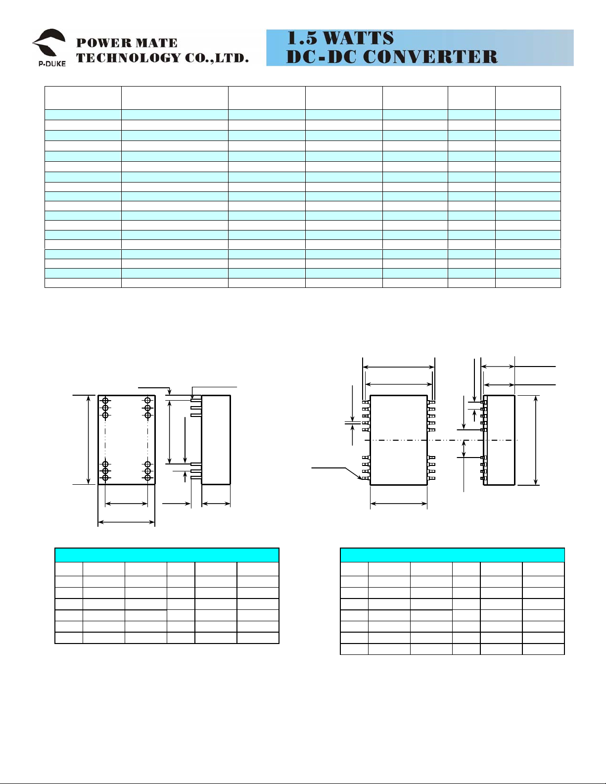
Dimensions
Weight
MTBF (Note 1) 5.531 x 10⁶ hrs
DIP
SMD
1.25 X 0.80 X 0.40 Inch
(31.8 X 20.3 X 10.2 mm)
9
10
ohms, min
16g (0.55oz)
18g (0.62oz)
ENVIRONMENTAL SPECIFICATIONS
Operating temperature range -25ºC ~ +71ºC
Maximum case temperature +100ºC
Storage temperature range -55ºC ~ +105ºC
Thermal impedance Nature convection 20ºC/watt
Thermal shock MIL-STD-810D
Vibration 10~55Hz, 10G, 30minutes along X,Y and Z
Relative humidity 5% to 95% RH
EMC CHARACTERISTICS
Conducted emissions EN55022 Class A
Radiated emissions EN55022 Class A
ESD EN61000-4-2 Perf. Criteria B
Radiated immunity EN61000-4-3 Perf. Criteria A
Fast transient EN61000-4-4 Perf. Criteria B
Surge EN61000-4-5 Perf. Criteria B
Conducted immunity EN61000-4-6 Perf. Criteria A
Model
Number
DR1P5-05S05 4.5 – 5.5 VDC 5 VDC 300mA
DR1P5-05S12 4.5 – 5.5 VDC 12 VDC 125mA
DR1P5-05S15 4.5 – 5.5 VDC 15 VDC 100mA
DR1P5-05D05 4.5 – 5.5 VDC ± 5 VDC 200mA/-100mA
DR1P5-05D12 4.5 – 5.5 VDC ± 12 VDC ± 60mA
DR1P5-05D15 4.5 – 5.5 VDC ± 15 VDC ± 50mA
DR1P5-12S05 10.8 – 13.2 VDC 5 VDC 300mA
DR1P5-12S12 10.8 – 13.2 VDC 12 VDC 125mA 260mA 52 330uF
DR1P5-12S15 10.8 – 13.2 VDC 15 VDC 100mA 245mA 55 330uF
DR1P5-12D05 10.8 – 13.2 VDC ± 5 VDC 200mA/-100mA 278mA 49 330uF
DR1P5-12D12 10.8 – 13.2 VDC ± 12 VDC ± 60mA 255mA 51 110uF
DR1P5-12D15 10.8 – 13.2 VDC ± 15 VDC ± 50mA 250mA 54 110uF
DR1P5-24S05 21.6 – 26.4 VDC 5 VDC 300mA 125mA 54 470uF
DR1P5-24S12 21.6 – 26.4 VDC 12 VDC 125mA 130mA 52 330uF
DR1P5-24S15 21.6 – 26.4 VDC 15 VDC 100mA 123mA 55 330uF
DR1P5-24D05 21.6 – 26.4 VDC ± 5 VDC 200mA/-100mA 142mA 48 330uF
DR1P5-24D12 21.6 – 26.4 VDC ± 12 VDC ± 60mA 128mA 51 110uF
DR1P5-24D15 21.6 – 26.4 VDC ± 15 VDC ± 50mA 125mA 54 110uF
Note
1. BELLCORE TR-NWT-000332. Case 1: 50% Stress , Temperature at 40ºC. (Ground fixed and controlled environment)
2. Maximum value at nominal input voltage and full load of standard type.
3. Typical value at nominal input voltage and full load.
4. Test by minimum Vin and constant resistive load.
Input
Range
Output
Voltage
Output
Current
Input
Current
600mA
625mA
588mA
682mA
613mA
600mA
245mA
(2)
Suffix-SMD
1.00(25.4)
0.92(23.4)
124
20
BOTTOM
VIEW
16
13
0.80(20.3)
5
9
12
SMD PIN CONNECTION
0.08(2.0)
24
1
23
2
22 3
0.01 x 0.02 (0.25 x 0.50)
Rectangular Pin
0.02(0.5)
0.90 (22.9)
1.25 (31.8)
15
10
14
11
13
12
0.60(15.2)
0.80(20.3)
PIN SINGLE DUAL
1 + INPUT + INPUT
2 NC - OUTPUT
3 NC COMMON
10 -OUTPUT COMMON
11 +OUTPUT +OUTPUT 14 +OUTPUT +OUTPUT
DIP PIN CONNECTION
0.10 (2.5)
0.15
(3.8)
0.40
(10.2)
1. All dimensions in Inches (mm)
Tolerance x.xx±0.02(x.x±0.5)
2. Pin pitch tolerance ±0.014(0.35)
DUAL SINGLE PIN
24 + INPUT + INPUT
23 NC - OUTPUT
22 NC COMMON
15 - OUTPUT COMMON
- INPUT- INPUT 13 - INPUT - INPUT 12
Pin Area
0.04 x 0.02
(1.0 x 0.5)
x.xxx±0.01(x.xx±0.25)
PIN SINGLE DUAL
1 + INPUT + INPUT
2 NC -OUTPUT
3 NC COMMON
10 -OUTPUT COMMON
11 +OUTPUT +OUTPUT 14 +OUTPUT +OUTPUT
12 -INPUT - INPUT 13 - INPUT - INPUT
VER:03 2 / 2
(3)
Eff
(%)
54 470uF
52 330uF
55 330uF
48 330uF
51 110uF
54 110uF
55 470uF
0.10 (2.54)
0.25 (6.35) 0.15 (3.81)
24 + INPUT + INPUT
23 NC -OUTPUT
22 NC COMMON
15 -OUTPUT COMMON
Others NCNCNC NCOthers
Capacitor
Load max
0.44(11.2)
0.43(10.9)
1.26 (32.0)
DUAL SINGLEPIN
(4)
 Loading...