

Power integrations TOP100-4, TOPSwitch series User Manual

TOP100-4
TOPSwitch
Three-terminal Off-line PWM Switch
AC
IN
DRAIN
SOURCE
CONTROL
TOPSwitch
TOPSwitch SELECTION GUIDE
OUTPUT POWER RANGE
ORDER
PART
NUMBER
N*
N*
N*
N*
N*
FLYBACK
100/110 V
VAC
48 V
DC
PFC/
BOOST
100/110
VAC
July 2009
TOP100-4
CONTROL
V
C
Z
C
SHUNT REGULATOR/
ERROR AMPLIFIER
-
+
5.7 V
5.7 V
4.7 V
SHUTDOWN/
AUTO-RESTART
+
-
POWER-UP
RESET
0
INTERNAL
SUPPLY
1
DRAIN
÷ 8
EXTERNALLY
TRIGGERED
SHUTDOWN
I
FB
OSCILLATOR
R
E
D
MAX
CLOCK
SAW
THERMAL
SHUTDOWN
COMPARATOR
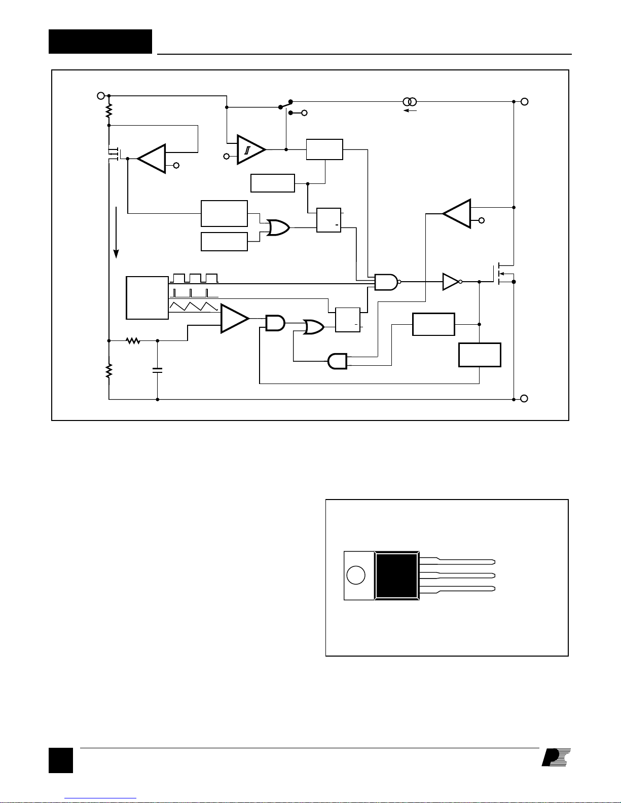
Figure 2. Functional Block Diagram.
Pin Functional Description
-
+
PWM
RSQ
Q
SRQ
+
-
V
I
LIMIT
CONTROLLED
TURN-ON
GATE
DRIVER
LEADING
Q
EDGE
BLANKING
MINIMUM
ON-TIME
DELAY
SOURCE
PI-1746-011796
DRAIN Pin:
Output MOSFET drain connection. Provides internal bias
current during start-up operation via an internal switched highvoltage current source. Internal current sense point.
CONTROL Pin:
Error amplifier and feedback current input pin for duty cycle
control. Internal shunt regulator connection to provide internal
bias current during normal operation. Trigger input for latching
shutdown. It is also used as the supply bypass and auto-restart/
compensation capacitor connection point.
SOURCE Pin:
Output MOSFET source connection. Primary-side circuit
common, power return, and reference point.
F
2
7 /09
DRAIN
SOURCE (TAB)
CONTROL
TO-220/3 (YO3A)
PI-1065A-110194
Figure 3. Pin Configuration.
TOP100-4
TOPSwitch
Family Functional Description
TOPSwitch is a self biased and protected
linear control current-to-duty cycle
converter with an open drain output.
High efficiency is achieved through the
use of CMOS and integration of the
maximum number of functions possible.
CMOS significantly reduces bias
currents as compared to bipolar or
discrete solutions. Integration eliminates
external power resistors used for current
sensing and/or supplying initial start-up
bias current.
During normal operation, the internal
output MOSFET duty cycle linearly
decreases with increasing CONTROL
pin current as shown in Figure 4. To
implement all the required control, bias,
and protection functions, the DRAIN
and CONTROL pins each perform
several functions as described below.
Refer to Figure 2 for a block diagram
and Figure 6 for timing and voltage
waveforms of the TOPSwitch integrated
circuit.
Control Voltage Supply
CONTROL pin voltage VC is the supply
or bias voltage for the controller and
driver circuitry. An external bypass
capacitor closely connected between the
CONTROL and SOURCE pins is
required to supply the gate drive current.
The total amount of capacitance
connected to this pin (CT) also sets the
auto-restart timing as well as control
loop compensation. VC is regulated in
either of two modes of operation.
Hysteretic regulation is used for initial
start-up and overload operation. Shunt
regulation is used to separate the duty
cycle error signal from the control circuit
supply current. During start-up, V
current is supplied from a high-voltage
switched current source connected
internally between the DRAIN and
CONTROL pins. The current source
provides sufficient current to supply the
control circuitry as well as charge the
total external capacitance (CT).
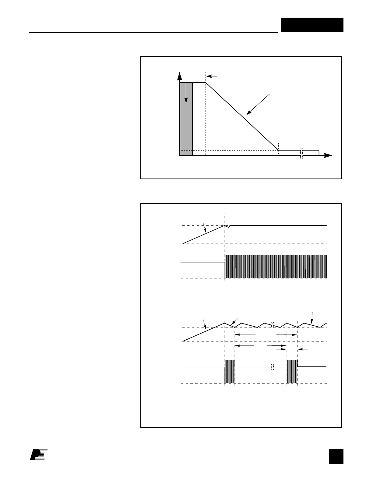
Auto-restart
I
D
MAX
B
Duty Cycle (%)
D
MIN
I
2.5 6.5 45
CD1
Figure 4. Relationship of Duty Cycle to CONTROL Pin Current.
IC
V
DRAIN
C
5.7 V
4.7 V
V
IN
Charging C
0
0
T
Off
(a)
IC
Charging C
5.7 V
4.7 V
V
C
0
C
DRAIN
V
IN
0
T
Off
Switching Switching
(b)
CT is the total external capacitance
connected to the CONTROL pin
Slope = PWM Gain
-16%/mA
IC (mA)
Switching
I
CD1
Discharging C
95%
Off
T
8 Cycles
Discharging C
5%
PI-1691-112895
I
CD2
T
Off
PI-1124A-060694
Figure 5. Start-up Waveforms for (a) Normal Operation and (b) Auto-restart.
7/ 09
F
3
V
IN
DRAIN
V
OUT
I
OUT
TOP100-4
V
IN
0
0
0
12 12 81
8
••• •••
V
C
0
12
I
0
C
1 2
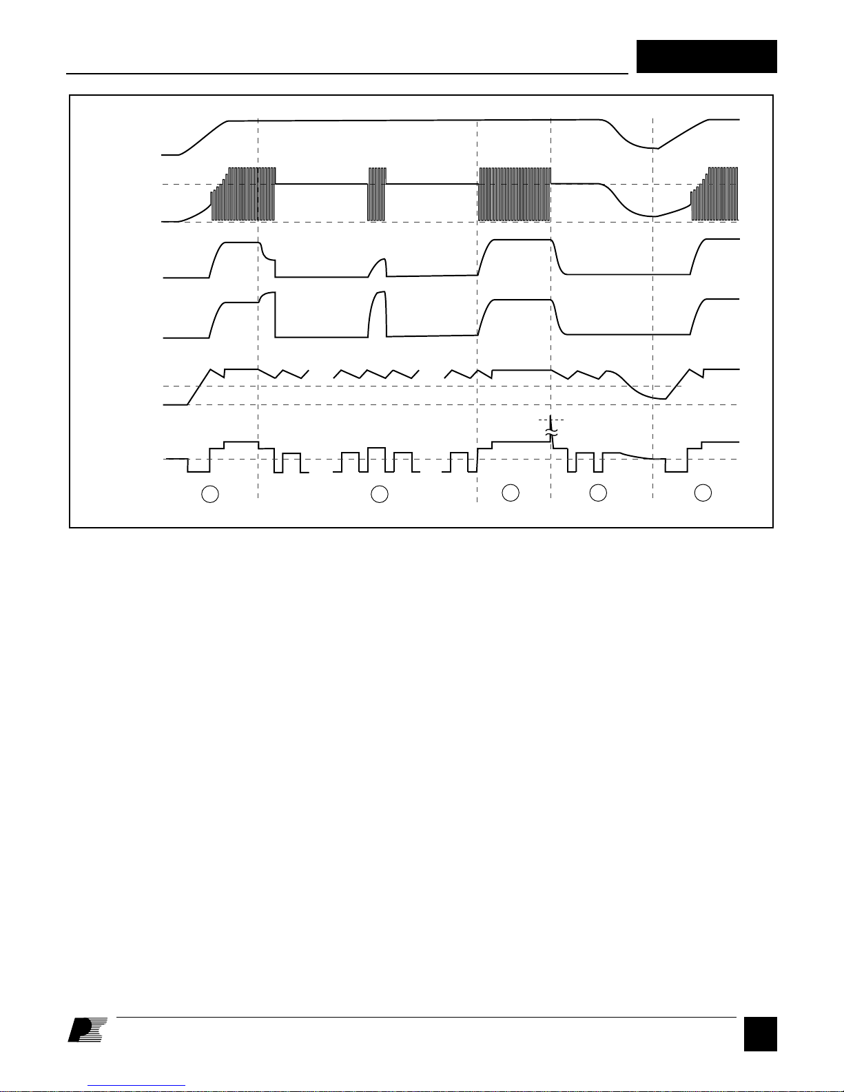
Figure 6. Typical Waveforms for (1) Normal Operation, (2) Auto-restart, (3) Latching Shutdown, and (4) Power Down Reset.
Shutdown/Auto-restart
To minimize TOPSwitch power
dissipation, the shutdown/auto-restart
circuit turns the power supply on and off
at a duty cycle of typically 5% if an out
of regulation condition persists. Loss of
regulation interrupts the external current
812 81
••• •••
removing and restoring input power, or
momentarily pulling the CONTROL pin
below the power-up reset threshold resets
the latch and allows TOPSwitch to
resume normal power supply operation.
VC is regulated in hysteretic mode when
the power supply is latched off.
into the CONTROL pin. VC regulation
changes from shunt mode to the
hysteretic auto-restart mode described
above. When the fault condition is
removed, the power supply output
becomes regulated, VC regulation returns
to shunt mode, and normal operation of
the power supply resumes.
Overtemperature Protection
Temperature protection is provided by a
precision analog circuit that turns the
output MOSFET off when the junction
temperature exceeds the thermal
shutdown temperature (typically 145°C).
Activating the power-up reset circuit by
removing and restoring input power or
Latching Shutdown
The output overvoltage protection latch
is activated by a high-current pulse into
the CONTROL pin. When set, the latch
turns off the TOPSwitch output.
Activating the power-up reset circuit by
momentarily pulling the CONTROL pin
below the power-up reset threshold resets
the latch and allows TOPSwitch to
resume normal power supply operation.
VC is regulated in hysteretic mode when
the power supply is latched off.
45 mA
High-voltage Bias Current Source
This current source biases TOPSwitch
from the DRAIN pin and charges the
CONTROL pin external capacitance
(CT) during start-up or hysteretic
operation. Hysteretic operation occurs
during auto-restart and latched
shutdown. The current source is switched
on and off with an effective duty cycle of
approximately 35%. This duty cycle is
determined by the ratio of CONTROL
pin charge (IC) and discharge currents
(I
CD1
and I
). This current source is
CD2
turned off during normal operation when
the output MOSFET is switching.
V
C(reset)
143
PI-1119-110194
7/ 09
F
5
TOP100-4
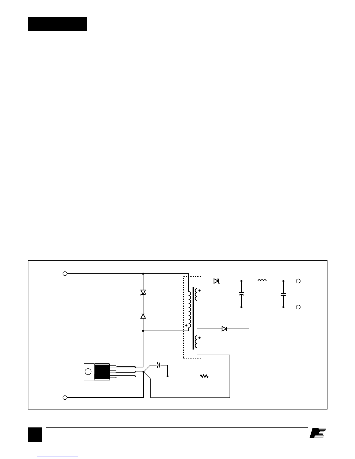
General Circuit Operation
Primary Feedback Regulation
The circuit shown in Figure 7 is a simple
5 V, 5 W bias supply using the TOP100.
This flyback power supply employs
primary-side regulation from a
transformer bias winding. This approach
is best for low-cost applications requiring
isolation and operation within a narrow
range of load variation. Line and load
regulation of ±5% or better can be
achieved from 10% to 100% of rated
load.
Voltage feedback is obtained from the
transformer (T1) bias winding, which
eliminates the need for optocoupler and
secondary-referenced error amplifier.
High-voltage DC is applied to the
primary winding of T1. The other side
of the transformer primary is driven by
the integrated high-voltage MOSFET
transistor within the TOP100 (U1). The
circuit operates at a switching frequency
of 100 kHz, set by the internal oscillator
of the TOP100. The clamp circuit
implemented by VR1 and D1 limits the
leading-edge voltage spike caused by
transformer leakage inductance to a safe
value. The 5 V power secondary winding
is rectified and filtered by D2, C2, C3,
and L1 to create the 5 V output voltage.
The output of the T1 bias winding is
rectified and filtered by D3, R1, and C5.
The voltage across C5 is regulated by
U1, and is determined by the 5.7 V
internal shunt regulator at the
CONTROL pin of U1. When the
rectified bias voltage on C5 begins to
exceed the shunt regulator voltage,
current will flow into the control pin.
Increasing control pin current decreases
the duty cycle until a stable operating
point is reached. The output voltage is
proportional to the bias voltage by the
turns ratio of the output to bias windings.
C5 is used to bypass the CONTROL pin.
C5 also provides loop compensation for
the power supply by shunting AC
currents around the CONTROL pin
dynamic impedance, and also determines
the auto-restart frequency during startup and auto-restart conditions. See DN8 for more information regarding bias
supplies.
D2
1N5822
VR1
P6KE91
D1
UF4004
C2
330 µF
25 V
D3
1N4148
DC
INPUT
C5
47 µF
DRAIN
SOURCE
CONTROL
U1
TOP100YAI
Figure 7. Schematic Diagram of a Minimum Parts Count 5 V, 5 W Bias Supply Utilizing the TOP100.
F
6
7 /09
T1
R1
22 Ω
L1
(Bead)
5 V
C3
150 µF
25 V
RTN
CIRCUIT PERFORMANCE:
Load Regulation - ±4%
(10% to 100%)
Line Regulation - ±1.5%
95 to 185 V DC
Ripple Voltage ±25 mV
PI-1767-020296
 Loading...