

April 1999
®
TOP412/414
TOPSwitch
Family
Three-terminal DC to DC PWM Switch
®
Product Highlights
Low Cost Replacement for Discrete Switchers
• Up to 15 fewer components - cuts cost, increases reliability
• Allows for a smaller and lighter solution under 12 mm
height, all surface mount components
Over 80% Efficiency in Flyback Topology
• Built-in start-up and current limit reduce DC losses
• Low capacitance MOSFET cuts switching losses
• CMOS controller/gate driver consumes only 7 mW
• 70% maximum duty cycle minimizes conduction losses
Simplifies Design - Reduces Time to Market
• Integrated PWM Controller and high power MOSFET
• Only one external capacitor needed for compensation,
bypass and start-up/auto-restart functions
System Level Fault Protection Features
• Auto-restart and cycle by cycle current limiting functions
handle both primary and secondary faults
• On-chip latching thermal shutdown protects the entire
system against overload
Highly Versatile
• Implements Buck, Boost, Flyback or Forward topology
• Easily interfaces with both opto and primary feedback
• Supports continuous or discontinuous mode of operation
• Specified for operation down to 16 V DC input
Description
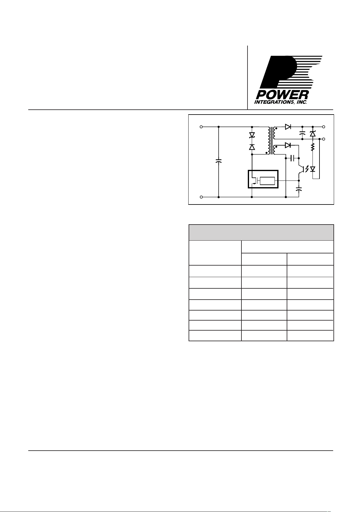
The TOPSwitch family implements, with only three terminals,
all functions necessary for a DC to DC, converter: high voltage
N-channel power MOSFET with controlled turn-on gate driver,
voltage mode PWM controller with integrated 120 kHz oscillator,
high voltage start-up bias circuit, bandgap derived reference,
bias shunt regulator/error amplifier for loop compensation and
fault protection circuitry. Compared to discrete MOSFET and
controller or self oscillating (RCC) switching converter solutions,
a TOPSwitch integrated circuit can reduce total cost, component
count, size, weight and at the same time increase efficiency and
system reliability. This device is well suited for Telecom,
Cablecom and other DC to DC converter applications up to
Figure 1. Typical Application.
MINIMUM
INPUT
VOLTAGE
ORDER PART NUMBER
Output Power Capability
1-4
18 VDC
3 W
9 W
TOP412G TOP414G
24 VDC
36 VDC
48 VDC
60 VDC
72 VDC
90 VDC
12 W
Table 1. TOP412/414 Output Power.
4 W
5 W 6 W
7 W 9 W
18 W
21 W
12 W 15 W
15 W 18 W
Notes: 1. Assumes maximum junction temperature of 100 °C
2. Assumes output of 5 V and KRP of 0.4 3. Soldered to 1 sq. inch
(645 mm2), 2 oz. copper clad (610 gm/mm2) 4. The continuous
power capability in a given application depends on thermal
environment, transformer design, efficiency required, input storage
capacity, etc.
PI-2371-120198
D
S
C
CONTROL
TOP414
V
IN
V
O
21W of output power. Internally, the lead frame of the
SMD-8 package uses six of its pins to transfer heat from the chip
directly to the board, eliminating the cost of a heat sink.
TOP412/414
A
4/99
2
PI-1746-011796
SHUTDOWN/
AUTO-RESTART
PWM
COMPARATOR
CLOCK
SAW
OSCILLATOR
CONTROLLED
TURN-ON
GATE
DRIVER
INTERNAL
SUPPLY
5.7 V
4.7 V
SOURCE
SRQ
Q
D
MAX
+
CONTROL
+
5.7 V
I
FB
R
E
Z
C
V
C
MINIMUM
ON-TIME
DELAY
+
-
V
I
LIMIT
LEADING
EDGE
BLANKING
POWER-UP
RESET
RSQ
Q
÷ 8
0
1
THERMAL
SHUTDOWN
EXTERNALLY
TRIGGERED
SHUTDOWN
SHUNT REGULATOR/
ERROR AMPLIFIER
+
-
DRAIN
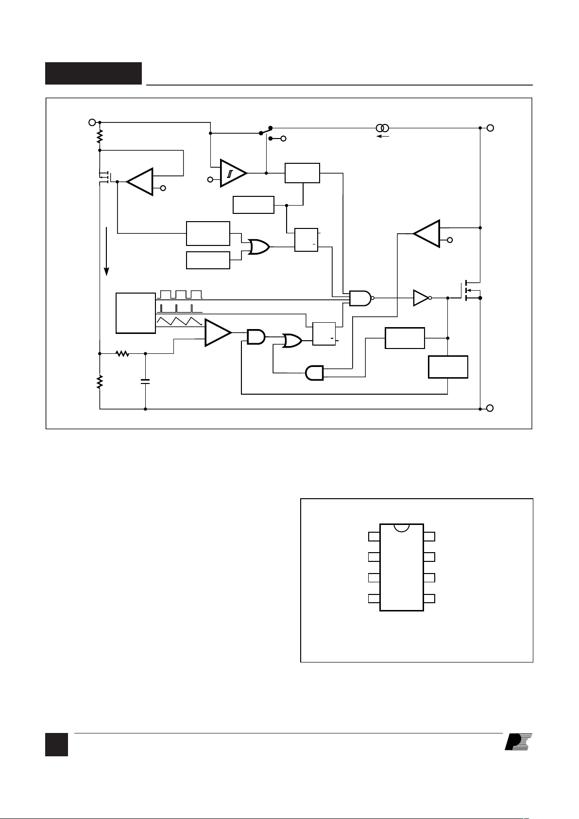
Figure 2. Functional Block Diagram.
Pin Functional Description
DRAIN Pin:
Output MOSFET drain connection. Provides internal bias
current during start-up operation via an internal switched highvoltage current source. Internal current sense point.
CONTROL Pin:
Error amplifier and feedback current input pin for duty cycle
control. Internal shunt regulator connection to provide internal
bias current during normal operation. Trigger input for latching
shutdown. It is also used as the supply bypass and auto-restart/
compensation capacitor connection point.
SOURCE Pin:
Output MOSFET source connection. Primary-side circuit
common, power return, and reference point.
Figure 3. Pin Configuration.
PI-2208-120798
CONTROL
8
5
7
6
DRAIN
SOURCE (HV RTN)
SOURCE
SOURCE
1
4
2
3
SOURCE (HV RTN)
SOURCE (HV RTN)
SOURCE
G Package (SMD-8)
A
4/99
TOP412/414
3
TOPSwitch
Family Functional Description
TOPSwitch is a self biased and protected linear control currentto-duty cycle converter with an open drain output. High
efficiency is achieved through the use of CMOS and integration
of the maximum number of functions possible. CMOS
significantly reduces bias currents as compared to bipolar or
discrete solutions. Integration eliminates external power resistors
used for current sensing and/or supplying initial start-up bias
current.
During normal operation, the internal output MOSFET duty
cycle linearly decreases with increasing CONTROL pin current
as shown in Figure 4. To implement all the required control,
bias, and protection functions, the DRAIN and CONTROL pins
each perform several functions as described below. Refer to
Figure 2 for a block diagram and Figure 6 for timing and voltage
waveforms of the TOPSwitch integrated circuit.
Control Voltage Supply
CONTROL pin voltage V
C
is the supply or bias voltage for the
controller and driver circuitry. An external bypass capacitor
closely connected between the CONTROL and SOURCE pins
is required to supply the gate drive current. The total amount of
capacitance connected to this pin (CT) also sets the auto-restart
timing as well as control loop compensation. VC is regulated in
either of two modes of operation. Hysteretic regulation is used
for initial start-up and overload operation. Shunt regulation is
used to separate the duty cycle error signal from the control
circuit supply current. During start-up, VC current is supplied
from a high-voltage switched current source connected internally
between the DRAIN and CONTROL pins. The current source
provides sufficient current to supply the control circuitry as
well as charge the total external capacitance (CT).
PI-1691-112895
D
MAX
D
MIN
I
CD1
Duty Cycle (%)
IC (mA)
2.5 6.5 45
Slope = PWM Gain
-16%/mA
I
B
Auto-restart
Figure 4. Relationship of Duty Cycle to CONTROL Pin Current.
Figure 5. Start-up Waveforms for (a) Normal Operation and (b)
Auto-restart.
DRAIN
0
V
IN
V
C
0
4.7 V
5.7 V
8 Cycles
95%
5%
Off
Switching Switching
Off
I
C
Charging C
T
I
CD1
Discharging C
T
I
CD2
Discharging C
T
I
C
Charging C
T
Off
PI-1124A-060694
DRAIN
0
V
IN
V
C
0
4.7 V
5.7 V
Off
Switching
(b)
(a)
CT is the total external capacitance
connected to the CONTROL pin

TOP412/414
A
4/99
4
TOPSwitch
Family Functional Description (cont.)
The first time VC reaches the upper threshold, the high-voltage
current source is turned off and the PWM modulator and output
transistor are activated, as shown in Figure 5(a). During normal
operation (when the output voltage is regulated) feedback
control current supplies the V
C
supply current. The shunt
regulator keeps VC at typically 5.7 V by shunting CONTROL
pin feedback current exceeding the required DC supply current
through the PWM error signal sense resistor RE. The low
dynamic impedance of this pin (ZC) sets the gain of the error
amplifier when used in a primary feedback configuration. The
dynamic impedance of the CONTROL pin together with the
external resistance and capacitance determines the control loop
compensation of the power system.
If the CONTROL pins total external capacitance (CT) should
discharge to the lower threshold, the output MOSFET is turned
off and the control circuit is placed in a low-current standby
mode. The high-voltage current source is turned on and charges
the external capacitance again. Charging current is shown with
a negative polarity and discharging current is shown with a
positive polarity in Figure 6. The hysteretic auto-restart
comparator keeps VC within a window of typically 4.7 to 5.7 V
by turning the high-voltage current source on and off as shown
in Figure 5(b). The auto-restart circuit has a divide-by-8
counter which prevents the output MOSFET from turning on
again until eight discharge-charge cycles have elapsed. The
counter effectively limits TOPSwitch power dissipation by
reducing the auto-restart duty cycle to typically 5%. Autorestart continues to cycle until output voltage regulation is again
achieved.
Bandgap Reference
All critical TOPSwitch internal voltages are derived from a
temperature-compensated bandgap reference. This reference
is also used to generate a temperature-compensated current
source which is trimmed to accurately set the oscillator frequency
and MOSFET gate drive current.
Oscillator
The internal oscillator linearly charges and discharges the
internal capacitance between two voltage levels to create a
sawtooth waveform for the pulse width modulator. The oscillator
sets the pulse width modulator/current limit latch at the beginning
of each cycle. The nominal frequency of 120 kHz was chosen
to minimize EMI and maximize efficiency in power supply
applications. Trimming of the current reference improves the
frequency accuracy.
Pulse Width Modulator
The pulse width modulator implements a voltage-mode control
loop by driving the output MOSFET with a duty cycle inversely
proportional to the current flowing into the CONTROL pin.
The error signal across RE is filtered by an RC network with a
typical corner frequency of 7 kHz to reduce the effect of
switching noise. The filtered error signal is compared with the
internal oscillator sawtooth waveform to generate the duty
cycle waveform. As the control current increases, the duty
cycle decreases. A clock signal from the oscillator sets a latch
which turns on the output MOSFET. The pulse width modulator
resets the latch, turning off the output MOSFET. The maximum
duty cycle is set by the symmetry of the internal oscillator. The
modulator has a minimum ON-time to keep the current
consumption of the TOPSwitch independent of the error signal.
Note that a minimum current must be driven into the CONTROL
pin before the duty cycle begins to change.
Gate Driver
The gate driver is designed to turn the output MOSFET on at a
controlled rate to minimize common-mode EMI. The gate
drive current is trimmed for improved accuracy.
Error Amplifier
The shunt regulator can also perform the function of an error
amplifier in primary feedback applications. The shunt regulator
voltage is accurately derived from the temperature compensated
bandgap reference. The gain of the error amplifier is set by the
CONTROL pin dynamic impedance. The CONTROL pin
clamps external circuit signals to the VC voltage level. The
CONTROL pin current in excess of the supply current is
separated by the shunt regulator and flows through RE as the
error signal.
Cycle-By-Cycle Current Limit
The cycle by cycle peak drain current limit circuit uses the
output MOSFET ON-resistance as a sense resistor. A current
limit comparator compares the output MOSFET ON-state
drain-source voltage, V
DS(ON),
with a threshold voltage. High
drain current causes V
DS(ON)
to exceed the threshold voltage and
turns the output MOSFET off until the start of the next clock
cycle. The current limit comparator threshold voltage is
temperature compensated to minimize variation of the effective
peak current limit due to temperature related changes in output
MOSFET R
DS(ON)
.
The leading edge blanking circuit inhibits the current limit
comparator for a short time after the output MOSFET is turned
on. The leading edge blanking time has been set so that current
spikes caused by primary-side capacitances and secondary-side
rectifier reverse recovery time will not cause premature
termination of the switching pulse.
Shutdown/Auto-restart
To minimize TOPSwitch power dissipation, the shutdown/
auto-restart circuit turns the power supply on and off at a duty
cycle of typically 5% if an out of regulation condition persists.
Loss of regulation interrupts the external current into the
A
4/99
TOP412/414
5
CONTROL pin. VC regulation changes from shunt mode to
the hysteretic auto-restart mode described above. When the
fault condition is removed, the power supply output becomes
regulated, VC regulation returns to shunt mode, and normal
operation of the power supply resumes.
Latching Shutdown
The output overvoltage protection latch is activated by a highcurrent pulse into the CONTROL pin. When set, the latch
turns off the TOPSwitch output. Activating the power-up
reset circuit by removing and restoring input power, or
momentarily pulling the CONTROL pin below the power-up
reset threshold resets the latch and allows TOPSwitch to
resume normal power supply operation. VC is regulated in
hysteretic mode when the power supply is latched off.
Over-Temperature Protection
Temperature protection is provided by a precision analog
circuit that turns the output MOSFET off when the junction
temperature exceeds the thermal shutdown temperature
(typically 145 °C). Activating the power-up reset circuit by
removing and restoring input power or momentarily pulling the
CONTROL pin below the power-up reset threshold resets the
latch and allows TOPSwitch to resume normal power supply
operation. VC is regulated in hysteretic mode when the power
supply is latched off.
High-voltage Bias Current Source
This current source biases TOPSwitch from the DRAIN pin and
charges the CONTROL pin external capacitance (CT) during
start-up or hysteretic operation. Hysteretic operation occurs
during auto-restart and latched shutdown. The current source
is switched on and off with an effective duty cycle of
approximately 35%. This duty cycle is determined by the ratio
of CONTROL pin charge (IC) and discharge currents (I
CD1
and
I
CD2
). This current source is turned off during normal operation
when the output MOSFET is switching.
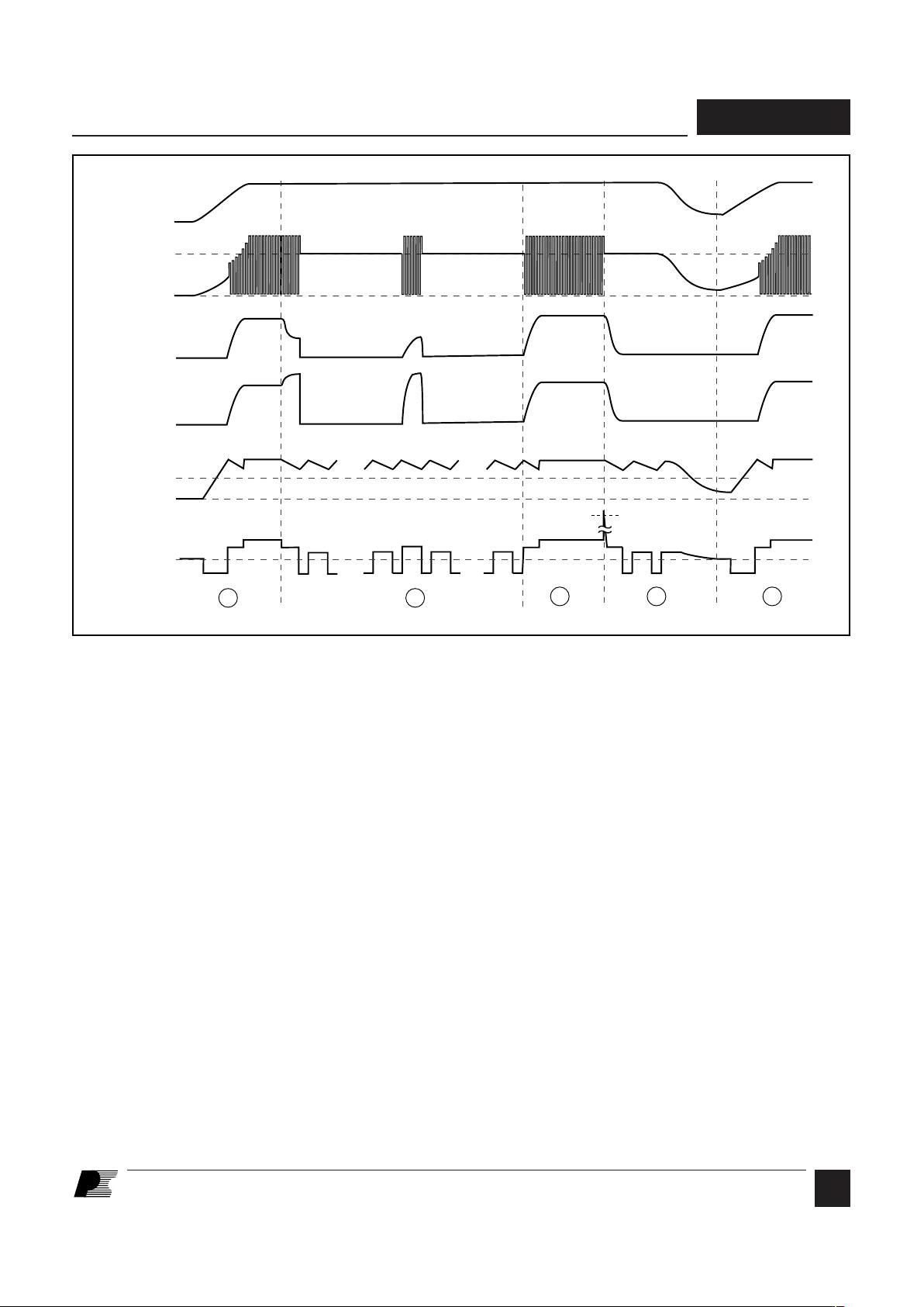
PI-1119-110194
V
IN
V
OUT
0
I
OUT
0
1 2
143
DRAIN
0
V
IN
V
C
0
• • • • • •
12 12 81
0
I
C
• • • • • •
12
8
812 81
V
C(reset)
45 mA
Figure 6. Typical Waveforms for (1) Normal Operation, (2) Auto-restart, (3) Latching Shutdown, and (4) Power Down Reset.

TOP412/414
A
4/99
6
Figure 7. Schematic Diagram of a 5 V, 10 W Isolated DC to DC Converter.
PI-2220-120998
D2
MBRD620CT
D3
1N4148
C3
330 µF
10 V
C5
330 µF
6.3 V
T1
D1
MURS120T3
VR1
ZGL41-100
U3
TL431ACD
R3
10k
C2
47 µF
U1
TOP414G
D
S
C
CONTROL
TOPSwitch
R1
15 Ω
L1
3.3 µH
C7
100 nF
U2
PC317A
R2
150 Ω
5 V
2.0 A
RTN
1
2
5
4
6, 7
9, 10
36-72 V
DC Input
C1
10 µF
100 V
C4
330 µF
10 V
C9
2.2 µF
C6
330 µF
6.3 V
R4
10k
C8
100 nF
C
X
100 nF
General Circuit Operation
Figure 7 shows a typical DC-DC converter application using
the TOP414G. This supply delivers 5 V at 2 A and works over
a wide input range from 36-72 VDC. The power supply
operates at an ambient temperature of 0-50 °C.
In order to achieve the highest possible efficiency and smallest
possible circuit board area, the primary and secondary current
waveform is shaped to have the lowest possible RMS and ripple
current. This is achieved by running very continuous and
utilizing the maximum duty cycle available.
For the example shown, the maximum component height is
12 mm. The EFD-20 transformer core was chosen to match this
maximum component height. The TOP414G has a high current
limit, which means that the EF20 core will saturate during
startup, until regulation is achieved. This is acceptable with the
TOP414G and does not cause device stress (provided the
maximum drain voltage is below 250 V peak and provided a
Zener is used for clamping). A Zener diode clamp circuit (VR1
and D1) is used in order to clamp the leakage inductance spike
to a fixed maximum voltage (an RCD, resistor capacitor diode,
clamp circuit would not be acceptable for this application).
In the example circuit, C1 provides local decoupling of the DC
input. This is required when the DC input source is distant from
this converter. A shottky diode (D2) with low voltage drop
provides secondary rectification and does not require additional
heat sinking (PC-board provides adequate heat sinking when
used with DPAK diode package). Tantalum capacitors (C3,C4)
provide low profile and small outline for secondary capacitance
(electrolytic capacitors can also be used as replacement).
Inductor L1 filters high frequency switching noise forming a π
filter with the output capacitors (C3-C6). The control loop gain
is set by resistor R2 and the stability is influenced by R1, C3 ,C4,
C5 and C6. Resistors R3 and R4 set the DC regulation point and
shunt regulator U3 along with bypass capacitor C8, provide the
drive for the optocoupler U2. Any remaining switching noise
in the system is filtered by ceramic capacitor C9.
Capacitor C2 and resistor R1 form part of the CONTROL pin
feedback circuit. Capacitor CX is used solely to decouple high
frequency noise on the control pin.

A
4/99
TOP412/414
7
Figure 8. Recommended TOPSwitch Layout.
PI-2210-102798
CONTROL
SOURCE
SOURCE
DRAIN
TOP VIEW
High Voltage
Return
Bias/Feedback
Return
Bias/Feedback
Input
G PACKAGE
Kelvin-connected
auto-restart/bypass capacitor C5
and/or compensation network
CONTROL pin transient
decoupling capacitor
Key Application Issues
Use a Kelvin connection to the SOURCE pin for the CONTROL
pin bypass capacitor. Use single point grounding techniques at
the SOURCE pin as shown in Figure 8. Use a ceramic high
frequency decoupling capacitor to bypass noise transients which
might appear on the CONTROL pin. The TOP412 and TOP414
have an over current latching shutdown feature. Failure to use
a high frequency decoupling capacitor may allow incidental
noise to accidentally trigger this feature.
Limit peak voltage and ringing on the DRAIN voltage at turnoff to a safe value. Use a Zener or TVS Zener diode to clamp
the DRAIN voltage.
Do not plug the TOPSwitch device into a “hot” IC socket during
test. External CONTROL pin capacitance may deliver a surge
current sufficient to trigger the shutdown latch which turns the
TOPSwitch off.
Under some conditions, externally provided bias or supply
current driven into the CONTROL pin can hold the TOPSwitch
in one of the 8 auto-restart cycles indefinitely and prevent
starting. Shorting the CONTROL pin to the SOURCE pin will
reset the TOPSwitch. To avoid this problem when doing bench
evaluations, it is recommended that the VC power supply be
turned on before the DRAIN voltage is applied.
CONTROL pin currents during auto-restart operation are much
lower at low input voltages (< 20 V) which increases the autorestart cycle period (see the IC vs. Drain Voltage Characteristic
curve).
In some cases, minimum loading may be necessary to keep a
lightly loaded or unloaded output voltage within the desired
range due to the minimum ON-time.
For additional applications information regarding the TOPSwitch
family, refer to Web site, www.powerint.com.

TOP412/414
A
4/99
8
Conditions
(Unless Otherwise Specified)
Specification Symbol See Figure 11 Min Typ Max Units
SOURCE = 0 V
TJ = -40 to 125 °C
ABSOLUTE MAXIMUM RATINGS
(1)
108 120 132
64 67 70
1.0 1.8 3.0
1.3 2.1 3.3
-21 -16 -11
-0.05
1.5 2.5 4
10 15 22
0.18
f
OSC
DC
MAX
DC
MIN
I
B
Z
C
CONTROL FUNCTIONS
Output
Frequency
Maximum
Duty Cycle
Minimum
Duty Cycle
PWM
Gain
PWM Gain
Temperature Drift
External
Bias Current
Dynamic
Impedance
Dynamic Impedance
Temperature Drift
kHz
%
%
%/mA
%/mA/°C
mA
Ω
%/°C
DRAIN Voltage ............................................ -0.3 to 350 V
CONTROL Voltage ..................................... - 0.3 V to 9 V
Storage Temperature .....................................-65 to 150 °C
Notes:
1. All voltages referenced to SOURCE, TA = 25 °C.
2. Normally limited by internal circuitry.
3. 1/16" from case for 5 seconds.
Operating Junction Temperature
(2)
................-40 to 150 °C
Lead Temperature
(3)
................................................ 260 °C
Thermal Impedance (θ
JA
) ...................................15 °C/W
(1)
Thermal Impedance (θJC) ..................................... 11 °C/W
THERMAL IMPEDANCE
TOP412
TOP414
IC = 4 mA, Tj = 25 °C
IC = I
CD1
+ 0.5 mA, See Figure 9
IC = 10 mA,
See Figure 9
IC = 4 mA, TJ = 25 °C
See Figure 4
See Note A
See Figure 4
IC = 4 mA, TJ = 25 °C
See Figure 10
1. Soldered to 1 sq. inch (645 mm2), 2 oz. (610 gm/m2) copper clad.

A
4/99
TOP412/414
9
-2.4 -1.9 -1.2
-2.0 -1.5 -0.8
0.4
5.7
4.7
0.6 1.0
58
1.2
2.00 2.90
2.95 4.25
150
100
125 145
25 45 75
2.0 3.3 4.2
T
J
= 25 °C
See Note A
S1 open
S1 open
S1 open
S1 open
S1 open
TOP412
di/dt = 400 mA/µs, TJ = 25 °C
TOP414
di/dt = 600 mA/µs, TJ = 25 °C
IC = 4 mA
IC = 4 mA
IC = 4 mA
See Figure 10
S2 open
I
LIMIT
t
LEB
t
ILD
I
SD
V
C(RESET)
mA
%/°C
V
V
V
%
Hz
A
ns
ns
°C
mA
V
SHUTDOWN/AUTO-RESTART
CONTROL Pin
Charging Current
Charging Current
Temperature Drift
Auto-restart
Threshold Voltage
UV Lockout
Threshold Voltage
Auto-restart
Hysteresis Voltage
Auto-restart
Duty Cycle
Auto-restart
Frequency
Self-protection
Current Limit
Leading Edge
Blanking Time
Current Limit
Delay
Thermal Shutdown
Temperature
Latched Shutdown
Trigger Current
Power-up Reset
Threshold Voltage
CIRCUIT PROTECTION
Conditions
(Unless Otherwise Specified)
Specification Symbol See Figure 11 Min Typ Max Units
SOURCE = 0 V
T
J
= -40 to 125 °C
VC = 0 V
VC = 5 V
V
C(AR)
I
C

TOP412/414
A
4/99
10
R
DS(ON)
I
DSS
BV
DSS
t
R
t
F
V
C(SHUNT)
I
CD1
I
CD2
ON-State
Resistance
OFF-State
Current
Breakdown
Voltage
Rise
Time
Fall
Time
DRAIN Supply
Voltage
Shunt Regulator
Voltage
Shunt Regulator
Temperature Drift
CONTROL Supply/
Discharge Current
Ω
µA
V
ns
ns
V
V
ppm/°C
mA
OUTPUT
SUPPLY
Conditions
(Unless Otherwise Specified)
Specification Symbol See Figure 11 Min Typ Max Units
SOURCE = 0 V
T
J
= -40 to 125 °C
2.6 3.0
4.2 5.0
1.7 2.0
2.8 3.3
500
350
100
50
36
5.5 5.8 6.1
±50
0.6 1.2 1.6
0.8 1.4 1.8
0.5 0.8 1.1
TOP412
TOP414
TOP412 TJ = 25 °C
ID = 270 mA TJ = 100 °C
TOP414 TJ = 25 °C
ID = 400 mA TJ = 100 °C
Device in Latched Shutdown
IC = 4 mA, VDS = 280 V, TA = 125 °C
Device in Latched Shutdown
IC = 4 mA, ID = 500 µA, TA = 25 °C
Measured With
Figure 7 Schematic
Measured With
Figure 7 Schematic
See Note B
IC = 4 mA
Output MOSFET Enabled
Output MOSFET Disabled

A
4/99
TOP412/414
11
Conditions
(Unless Otherwise Specified)
Specification Symbol See Figure 11 Min Typ Max Units
VS2 = 16 V R1 = 0 Ω
SOURCE = 0 V
TJ = -40 to 125 °C
LOW INPUT VOLTAGE OPERATION (See Note C)
Volts
mA
mA
%
Hz
DRAIN Supply
Voltage
CONTROL Pin
Charging Current
Auto-restart
Duty Cycle
Auto-restart
Frequency
NOTES:
A. For specifications with negative values, a negative temperature coefficient corresponds to an increase in
magnitude with increasing temperature, and a positive temperature coefficient corresponds to a decrease in
magnitude with increasing temperature.
B. It is possible to start up and operate TOPSwitch at DRAIN voltages well below 36 V. Refer to the "Low Input
Voltage" Specification section for details.
C.This section specifies only parameters affected by low input voltage operation (Drain Voltages less than 36 V). All
other parameters remain unchanged.
D. For low input voltage applications, the primary peak current could be set to a lower value than the current limit to
increase efficiency. Refer to the Output Characteristics graph (Drain Current vs. Drain Voltage). The voltage
across the transformer primary during the ON time is the difference between the input voltage and the drain
voltage (V
DS(ON)
).
For example, if the input voltage is 16 VDC and a TOP414 (2.95 A minimum current limit) is used at a primary
peak current of 1A. Then the (V
DS(ON)
) is 3 V at 100 °C and the energizing voltage across the transformer
primary is 13 V.
S1/Open
S1/Open
See Note D
T
J
= 25 °C
16
-2.30 -1.65 -1.00
-1.20 -0.64 -0.28
48
0.85
VC= 0 V
V
C
= 5 V

TOP412/414
A
4/99
12
Figure 9. TOPSwitch Duty Cycle Measurement.
Figure 11. TOPSwitch General Test Circuit.
120
100
80
40
20
60
0
0246810
CONTROL Pin Voltage (V)
CONTROL Pin Current (mA)
TYPICAL CONTROL PIN I-V CHARACTERISTIC
PI-1216-091794
Latched Shutdown
Trigger Current (45 mA)
1
Slope
Dynamic
Impedance
=
Figure 10. TOPSwitch CONTROL Pin I-V Characteristic.
PI-2212-073098
C1
0.1 µF
C2
47 µF
VS1
0-50 V
VS2
40 V
R1
470 Ω
5 W
S2
S1
R2
470 Ω
NOTES: 1. This test circuit is not applicable for current limit or output characteristic measurements.
2. For P package, short all SOURCE and SOURCE (HV RTN) pins together.
D
S
C
CONTROL
TOPSwitch
PI-1215-091794
DRAIN
VOLTAGE
HV
0 V
90%
10%
90%
t
2
t
1
DC =
t
1
t
2

A
4/99
TOP412/414
13
The following precautions should be followed when testing
TOPSwitch by itself outside of a power supply. The schematic
shown in Figure 11 is suggested for laboratory testing of
TOPSwitch.
When the DRAIN supply is turned on, the part will be in the
auto-restart mode. The CONTROL pin voltage will be oscillating
at a low frequency from 4.7 to 5.7 V and the DRAIN is turned
on every eighth cycle of the CONTROL pin oscillation. If the
BENCH TEST PRECAUTIONS FOR EVALUATION OF ELECTRICAL CHARACTERISTICS
Typical Performance Characteristics
CONTROL pin power supply is turned on while in this autorestart mode, there is only a 12.5% chance that the CONTROL
pin oscillation will be in the correct state (DRAIN active state)
so that the continuous DRAIN voltage waveform may be
observed. It is recommended that the VC power supply be
turned on first and the DRAIN power supply second if continuous
drain voltage waveforms are to be observed. The 12.5% chance
of being in the correct state is due to the 8:1 counter.
1.1
1.0
0.9
-50 -25 0 25 50 75 100 125 150
Junction Temperature (°C)
Breakdown Voltage (V)
(Normalized to 25 °C)
BREAKDOWN vs. TEMPERATURE
PI-176B-051391
1.2
1.0
0.8
0.6
0.4
0.2
0
-50 -25 0 25 50 75 100 125 150
Junction Temperature (°C)
FREQUENCY vs. TEMPERATURE
PI-1123A-060794
Output Frequency
(Normalized to 25 °C)
1.2
1.0
0.8
0.6
0.4
0.2
0
-50 -25 0 25 50 75 100 125 150
Junction Temperature (°C)
CURRENT LIMIT vs. TEMPERATURE
PI-1125-041494
Current Limit
(Normalized to 25 °C)
2
1.2
1.6
0
0 20406080100
Drain Voltage (V)
CONTROL Pin
Charging Current (mA)
IC vs. DRAIN VOLTAGE
PI-1145-103194
0.4
0.8
VC = 5 V

TOP412/414
A
4/99
14
Typical Performance Characteristics (cont.)
5
3
4
0
0
4682 10
Drain Current (A)
OUTPUT CHARACTERISTICS
PI-2214-120198
1
2
Drain Voltage (V)
T
CASE
= 25 °C
T
CASE
= 100 °C
Scaling Factors:
TOP414 1.00
TOP412 0.67
1000
10
0 24016080 320
DRAIN Voltage (V)
DRAIN Capacitance (pF)
C
OSS
vs. DRAIN VOLTAGE
100
PI-2216-120198
Scaling Factors:
TOP414 1.00
TOP412 0.67
100
50
0
0 16080 240 320
DRAIN Voltage (V)
Power (mW)
DRAIN CAPACITANCE POWER
PI-2218-120195
Scaling Factors:
TOP414 1.00
TOP412 0.67

A
4/99
TOP412/414
15
PI-2077-042601
1
A
J1
4
L
85
C
G08A
SMD-8
D S .004 (.10)
J2
E S .010 (.25)
-E-
-D-
B
-F-
M
J3
DIM
A
B
C
G
H
J1
J2
J3
J4
K
L
M
P
α
inches
0.370-0.385
0.245-0.255
0.125-0.135
0.004-0.012
0.036-0.044
0.060 (NOM)
0.048-0.053
0.032-0.037
0.007-0.011
0.010-0.012
0.100 BSC
0.030 (MIN)
0.372-0.388
0-8°
mm
9.40-9.78
6.22-6.48
3.18-3.43
0.10-0.30
0.91-1.12
1.52 (NOM)
1.22-1.35
0.81-0.94
0.18-0.28
0.25-0.30
2.54 BSC
0.76 (MIN)
9.45-9.86
0-8°
Notes:
1. Package dimensions conform to JEDEC
specification MS-001-AB (issue B, 7/85)
except for lead shape and size.
2. Controlling dimensions are inches.
3. Dimensions shown do not include mold
flash or other protrusions. Mold flash or
protrusions shall not exceed .006 (.15) on
any side.
4. D, E and F are reference datums on the
molded body.
K
G
α
H
.004 (.10)
J4
P
.010 (.25) M A S
Heat Sink is 2 oz. Copper
As Big As Possible
.420
.046
.060
.060
.046
.080
Pin 1
.086
.186
.286
Solder Pad Dimensions

TOP412/414
A
4/99
16
KOREA
Power Integrations
International Holdings, Inc.
Rm# 402, Handuk Building
649-4 Yeoksam-Dong,
Kangnam-Gu,
Seoul, Korea
Phone: +82-2-568-7520
Fax: +82-2-568-7474
e-mail: koreasales@powerint.com
WORLD HEADQUARTERS
AMERICAS
Power Integrations, Inc.
5245 Hellyer Avenue
San Jose, CA 95138 USA
Main: +1 408-414-9200
Customer Service:
Phone: +1 408-414-9665
Fax: +1 408-414-9765
e-mail: usasales@powerint.com
For the latest updates, visit our Web site: www.powerint.com
Power Integrations reserves the right to make changes to its products at any time to improve reliability or manufacturability.
Power Integrations does not assume any liability arising from the use of any device or circuit described herein, nor does it
convey any license under its patent rights or the rights of others.
The PI Logo,
TOPSwitch, TinySwitch
and
EcoSmart
are registered trademarks of Power Integrations, Inc.
©Copyright 2001, Power Integrations, Inc.
JAPAN
Power Integrations, K.K.
Keihin-Tatemono 1st Bldg.
12-20 Shin-Yokohama 2-Chome
Kohoku-ku, Yokohama-shi
Kanagawa 222-0033, Japan
Phone: +81-45-471-1021
Fax: +81-45-471-3717
e-mail: japansales@powerint.com
TAIWAN
Power Integrations
International Holdings, Inc.
17F-3, No. 510
Chung Hsiao E. Rd.,
Sec. 5,
Taipei, Taiwan 110, R.O.C.
Phone: +886-2-2727-1221
Fax: +886-2-2727-1223
e-mail: taiwansales@powerint.com
EUROPE & AFRICA
Power Integrations (Europe) Ltd.
Centennial Court
Easthampstead Road
Bracknell
Berkshire, RG12 1YQ
United Kingdom
Phone: +44-1344-462-300
Fax: +44-1344-311-732
e-mail: eurosales@powerint.com
CHINA
Power Integrations
International Holdings, Inc.
Rm# 1705, Bao Hua Bldg.
1016 Hua Qiang Bei Lu
Shenzhen, Guangdong 518031
China
Phone: +86-755-367-5143
Fax: +86-755-377-9610
e-mail: chinasales@powerint.com
INDIA (Technical Support)
Innovatech
#1, 8th Main Road
Vasanthnagar
Bangalore, India 560052
Phone: +91-80-226-6023
Fax: +91-80-228-9727
e-mail: indiasales@powerint.com
APPLICATIONS HOTLINE
World Wide +1-408-414-9660
APPLICATIONS FAX
World Wide +1-408-414-9760
 Loading...