

Power Integrations TNY268P, TNY268G, TNY267P, TNY266P, TNY267G Datasheet
...
TNY264/266-268
®
®
TinySwitch-II
Enhanced, Energy Efficient,
Low Power Off-line Switcher
Family
Product Highlights
TinySwitch-II
• Fully integrated auto-restart for short circuit and open
loop fault protection–saves external component costs
• Built-in circuitry practically eliminates audible noise with
ordinary varnished transformer
• Programmable line under-voltage detect feature prevents
power on/off glitches–saves external components
• Frequency jittering dramatically reduces EMI (~10 dB)
–minimizes EMI filter component costs
• 132 kHz operation reduces transformer size–allows use of
EF12.6 or EE13 cores for low cost and small size
• Very tight tolerances and negligible temperature variation
on key parameters eases design and lowers cost
• Lowest component count switcher solution
Better Cost/Performance over RCC & Linears
• Lower system cost than RCC, discrete PWM and other
integrated/hybrid solutions
• Cost effective replacement for bulky regulated linears
• Simple ON/OFF control–no loop compensation needed
• No bias winding–simpler, lower cost transformer
EcoSmart
• No load consumption < 50 mW with bias winding and
< 250 mW without bias winding at 265 VAC input
• Meets Blue Angel, Energy Star, and EC requirements
• Ideal for cell-phone charger and PC standby applications
High Performance at Low Cost
• High voltage powered–ideal for charger applications
• High bandwidth provides fast turn on with no overshoot
• Current limit operation rejects line frequency ripple
• Built-in current limit and thermal protection
Features Reduce System Cost
®
–Extremely Energy Efficient
Description
TinySwitch-II maintains the simplicity of the TinySwitch
topology, while providing a number of new enhancements to
further reduce system cost and component count, and to
practically eliminate audible noise. Like TinySwitch, a 700 V
power MOSFET, oscillator, high voltage switched current source,
current limit and thermal shutdown circuitry are integrated onto a
monolithic device. The start-up and operating power are derived
directly from the voltage on the DRAIN pin, eliminating the
need for a bias winding and associated circuitry. In addition, the
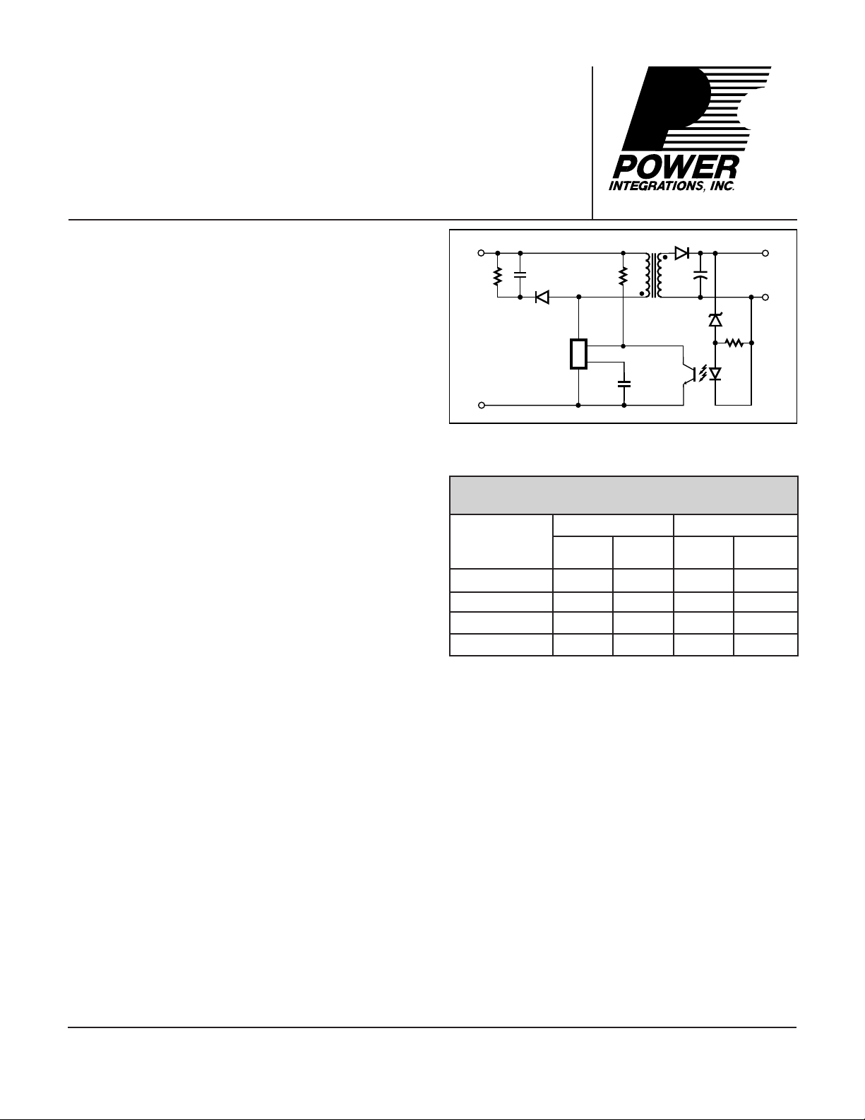
+
Optional
UV Resistor
Wide-Range
HV DC Input
TinySwitch-II
-
Figure 1. Typical Standby Application.
D
EN/UV
BP
S
+
DC Output
-
PI-2684-101700
OUTPUT POWER TABLE
230 VAC ±15%
PRODUCT
TNY264P or G
TNY266P or G
TNY267P or G
TNY268P or G
T able 1. Notes: 1. T ypical continuous power in a non-ventilated enclosed
adapter measured at 50 ˚C ambient. 2. Maximum practical continuous
power in an open frame design with adequate heat sinking, measured at
50 ˚C ambient (See key applications section for details). 3. Packages:
P: DIP-8B, G: SMD-8B. Please see part ordering information.
(3)
Adapter
(1)
Open
Frame
(2)
5.5 W 9 W 4 W 6 W
10 W 15 W 6 W 9.5 W
13 W 19 W 8 W 12 W
16 W 23 W 10 W 15 W
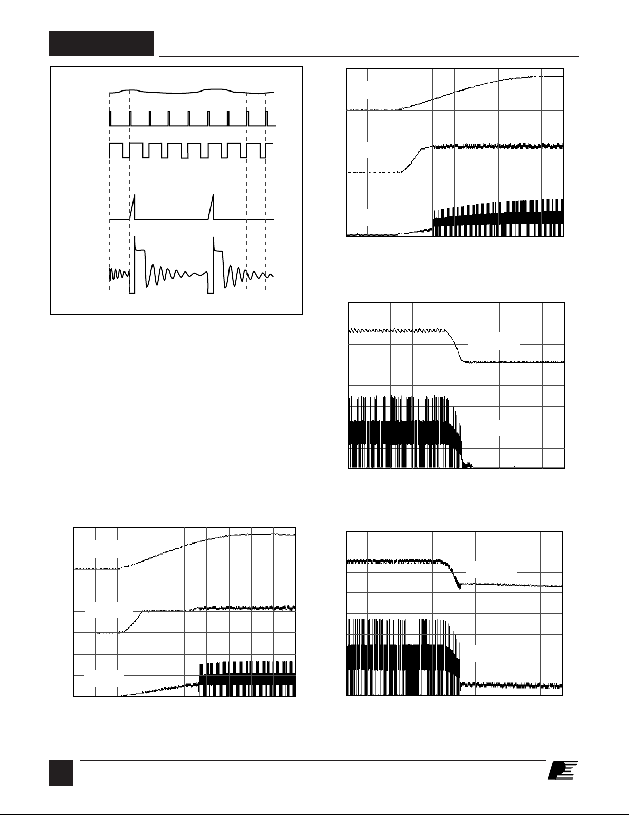
TinySwitch-II devices incorporate auto-restart, line undervoltage sense, and frequency jittering. An innovative design
minimizes audio frequency components in the simple ON/OFF
control scheme to practically eliminate audible noise with
standard taped/varnished transformer construction. The fully
integrated auto-restart circuit safely limits output power during
fault conditions such as output short circuit or open loop,
reducing component count and secondary feedback circuitry
cost. An optional line sense resistor externally programs a line
under-voltage threshold, which eliminates power down glitches
caused by the slow discharge of input storage capacitors present
in applications such as standby supplies. The operating frequency
of 132 kHz is jittered to significantly reduce both the quasi-peak
and average EMI, minimizing filtering cost.
85-265 VAC
Adapter
(1)
Open
Frame
(2)
July 2001
TNY264/266-268
BYPASS
(BP)
240 µA 50 µA
ENABLE
1.0 V + V
ENABLE/
UNDER-
VOLTAGE
(EN/UV)
1.0 V
DRAIN
REGULATOR
5.8 V
LINE UNDER-VOLTAGE
FAULT
RESET
MAX
PRESENT
CURRENT
LIMIT STATE
MACHINE
5.8 V
4.8 V
THERMAL
SHUTDOWN
SRQ
Q
AUTO-
RESTART
COUNTER
6.3 V
JITTER
CLOCK
T
DC
OSCILLATOR
BYPASS PIN
UNDER-VOLTAGE
+
-
V
I
LIMIT
CURRENT LIMIT
COMPARATOR
LEADING
EDGE
BLANKING
+
(D)
Figure 2. Functional Block Diagram.
Pin Functional Description
DRAIN (D) Pin:
Power MOSFET drain connection. Provides internal operating
current for both start-up and steady-state operation.
BYPASS (BP) Pin:
Connection point for a 0.1 µF external bypass capacitor for the
internally generated 5.8 V supply.
ENABLE/UNDER-VOLTAGE (EN/UV) Pin:
This pin has dual functions: enable input and line under-voltage
sense. During normal operation, switching of the power
MOSFET is controlled by this pin. MOSFET switching is
terminated when a current greater than 240 µA is drawn from
this pin. This pin also senses line under-voltage conditions
through an external resistor connected to the DC line voltage.
If there is no external resistor connected to this pin,
TinySwitch-II detects its absence and disables the line undervoltage function.
SOURCE
(S)
PI-2643-030701
P Package (DIP-8B)
G Package (SMD-8B)
BP
1
S
2
S
3
EN/UV
4
Figure 3. Pin Configuration.
S (HV RTN)
8
7
S (HV RTN)
5
D
PI-2685-101600
SOURCE (S) Pin:
Control circuit common, internally connected to output
MOSFET source.
SOURCE (HV RTN) Pin:
Output MOSFET source connection for high voltage return.
B
2
7/01
TNY264/266-268
TinySwitch-II
Functional Description
TinySwitch-II combines a high voltage power MOSFET switch
with a power supply controller in one device. Unlike conventional
PWM (Pulse Width Modulator) controllers, TinySwitch-II uses
a simple ON/OFF control to regulate the output voltage.
The TinySwitch-II controller consists of an Oscillator, Enable
Circuit (Sense and Logic), Current Limit State Machine, 5.8 V
Regulator, Bypass pin Under-Voltage Circuit, Over
Temperature Protection, Current Limit Circuit, Leading Edge
Blanking and a 700 V power MOSFET. TinySwitch-II
incorporates additional circuitry for Line Under-Voltage Sense,
Auto-Restart and Frequency Jitter. Figure 2 shows the functional
block diagram with the most important features.
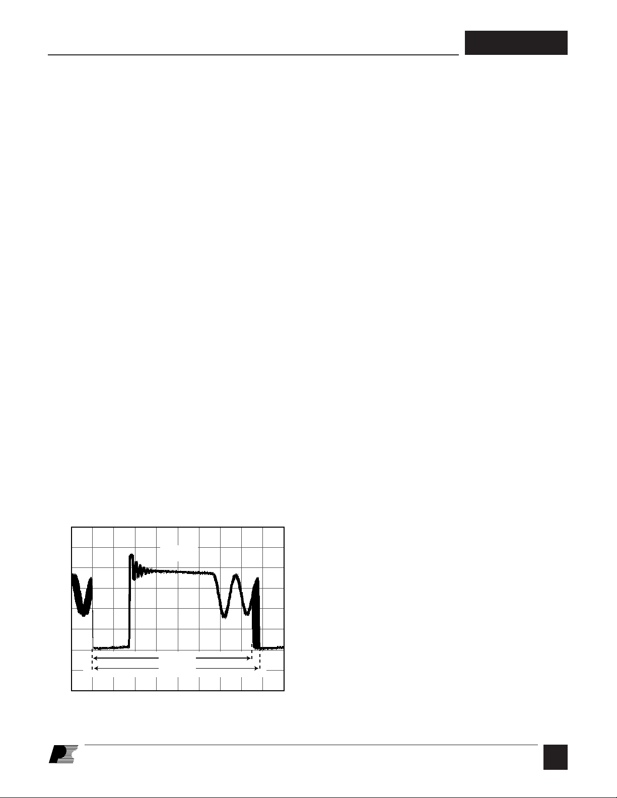
Oscillator
The typical oscillator frequency is internally set to an average
of 132 kHz. Two signals are generated from the oscillator: the
Maximum Duty Cycle signal (DC
) and the Clock signal that
MAX
indicates the beginning of each cycle.
The TinySwitch-II oscillator incorporates circuitry that
introduces a small amount of frequency jitter, typically 8 kHz
peak-to-peak, to minimize EMI emission. The modulation rate
of the frequency jitter is set to 1 kHz to optimize EMI reduction
for both average and quasi-peak emissions. The frequency jitter
should be measured with the oscilloscope triggered at the
falling edge of the DRAIN waveform. The waveform in Figure4
illustrates the frequency jitter of the TinySwitch-II.
Enable Input and Current Limit State Machine
The enable input circuit at the EN/UV pin consists of a low
impedance source follower output set at 1.0 V. The current
through the source follower is limited to 240 µA. When the
current out of this pin exceeds 240 µA, a low logic level
(disable) is generated at the output of the enable circuit. This
enable circuit output is sampled at the beginning of each cycle
on the rising edge of the clock signal. If high, the power
MOSFET is turned on for that cycle (enabled). If low, the power
MOSFET remains off (disabled). Since the sampling is done
only at the beginning of each cycle, subsequent changes in the
EN/UV pin voltage or current during the remainder of the cycle
are ignored.
The Current Limit State Machine reduces the current limit by
discrete amounts at light loads when TinySwitch-II is likely to
switch in the audible frequency range. The lower current limit
raises the effective switching frequency above the audio range
and reduces the transformer flux density including the associated
audible noise. The state machine monitors the sequence of
EN/UV pin voltage levels to determine the load condition and
adjusts the current limit level accordingly in discrete amounts.
Under most operating conditions (except when close to noload), the low impedance of the source follower keeps the
voltage on the EN/UV pin from going much below 1.0 V in the
disabled state. This improves the response time of the optocoupler
that is usually connected to this pin.
5.8 V Regulator and 6.3 V Shunt Voltage Clamp
The 5.8 V regulator charges the bypass capacitor connected to
the BYPASS pin to 5.8 V by drawing a current from the voltage
on the DRAIN pin, whenever the MOSFET is off. The
BYPASS pin is the internal supply voltage node for the
TinySwitch-II. When the MOSFET is on, the TinySwitch-II
operates from the energy stored in the bypass capacitor.
Extremely low power consumption of the internal circuitry
allows TinySwitch-II to operate continuously from current it
takes from the DRAIN pin. A bypass capacitor value of 0.1 µF
is sufficient for both high frequency decoupling and energy
storage.
600
500
400
300
200
100
0
0
Figure 4. Frequency Jitter.
In addition, there is a 6.3 V shunt regulator clamping the
BYPASS pin at 6.3 V when current is provided to the BYPASS
V
DRAIN
PI-2741-041901
pin through an external resistor. This facilitates powering of
TinySwitch-II externally through a bias winding to decrease the
no load consumption to about 50 mW.
BYPASS Pin Under-Voltage
The BYPASS pin under-voltage circuitry disables the power
MOSFET when the BYPASS pin voltage drops below 4.8 V.
Once the BYPASS pin voltage drops below 4.8 V, it must rise
back to 5.8 V to enable (turn-on) the power MOSFET.
136 kHz
128 kHz
510
Time (µs)
7/01
B
3

TNY264/266-268
Over Temperature Protection
The thermal shutdown circuitry senses the die temperature. The
threshold is typically set at 135 °C with 70 °C hysteresis. When
the die temperature rises above this threshold the power
MOSFET is disabled and remains disabled until the die
temperature falls by 70 °C, at which point it is re-enabled. A
large hysteresis of 70 °C (typical) is provided to prevent
overheating of the PC board due to a continuous fault condition.
Current Limit
The current limit circuit senses the current in the power MOSFET.
When this current exceeds the internal threshold (I
LIMIT
), the
power MOSFET is turned off for the remainder of that cycle.
The current limit state machine reduces the current limit threshold
by discrete amounts under medium and light loads.
The leading edge blanking circuit inhibits the current limit
comparator for a short time (t
) after the power MOSFET is
LEB
turned on. This leading edge blanking time has been set so that
current spikes caused by capacitance and secondary-side rectifier
reverse recovery time will not cause premature termination of
the switching pulse.
Auto-Restart
In the event of a fault condition such as output overload, output
short circuit, or an open loop condition, TinySwitch-II enters
into auto-restart operation. An internal counter clocked by the
oscillator gets reset every time the EN/UV pin is pulled low. If
the EN/UV pin is not pulled low for 50 ms, the power MOSFET
switching is normally disabled for 850 ms (except in the case of
line under-voltage condition in which case it is disabled until
the condition is removed). The auto-restart alternately enables
and disables the switching of the power MOSFET until the fault
condition is removed. Figure 5 illustrates auto-restart circuit
operation in the presence of an output short circuit.
In the event of a line under-voltage condition, the switching of
the power MOSFET is disabled beyond its normal 850 ms time
until the line under-voltage condition ends.
Line Under-Voltage Sense Circuit
The DC line voltage can be monitored by connecting an
external resistor from the DC line to the EN/UV pin. During
power-up or when the switching of the power MOSFET is
disabled in auto-restart, the current into the EN/UV pin must
exceed 50 µA to initiate switching of the power MOSFET.
During power-up, this is implemented by holding the BYPASS
pin to 4.8 V while the line under-voltage condition exists. The
BYPASS pin then rises from 4.8 V to 5.8V when the line undervoltage condition goes away. When the switching of the power
MOSFET is disabled in auto-restart mode and a line undervoltage condition exists, the auto-restart counter is stopped.
This stretches the disable time beyond its normal 850ms until
the line under-voltage condition ends.
The line under-voltage circuit also detects when there is no
external resistor connected to the EN/UV pin (less than ~ 2 µA
into pin). In this case the line under-voltage function is disabled.
TinySwitch-II
Operation
TinySwitch-II devices operate in the current limit mode. When
enabled, the oscillator turns the power MOSFET on at the
beginning of each cycle. The MOSFET is turned off when the
current ramps up to the current limit or when the DC
MAX
limit is
reached. As the highest current limit level and frequency of a
TinySwitch-II design are constant, the power delivered to the
load is proportional to the primary inductance of the transformer
and peak primary current squared. Hence, designing the supply
involves calculating the primary inductance of the transformer
for the maximum output power required. If the TinySwitch-II is
appropriately chosen for the power level, the current in the
calculated inductance will ramp up to current limit before the
DC
limit is reached.
MAX
300
200
100
0
10
5
0
0
Figure 5. TinySwitch-II Auto-Restart Operation.
B
4
7/01
V
DRAIN
V
DC-OUTPUT
1000 2000
Time (ms)
Enable Function
TinySwitch-II senses the EN/UV pin to determine whether or
not to proceed with the next switch cycle as described earlier.
PI-2699-030701
The sequence of cycles is used to determine the current limit.
Once a cycle is started, it always completes the cycle (even
when the EN/UV pin changes state half way through the cycle).
This operation results in a power supply in which the output
voltage ripple is determined by the output capacitor, amount of
energy per switch cycle and the delay of the feedback.
The EN/UV pin signal is generated on the secondary by
comparing the power supply output voltage with a reference
voltage. The EN/UV pin signal is high when the power supply
output voltage is less than the reference voltage.
In a typical implementation, the EN/UV pin is driven by an
optocoupler. The collector of the optocoupler transistor
isconnected to the EN/UV pin and the emitter is connected to
TNY264/266-268
the SOURCE pin. The optocoupler LED is connected in series
with a Zener diode across the DC output voltage to be regulated.
When the output voltage exceeds the target regulation voltage
level (optocoupler LED voltage drop plus Zener voltage), the
optocoupler LED will start to conduct, pulling the EN/UV pin
low. The Zener diode can be replaced by a TL431 reference
circuit for improved accuracy.
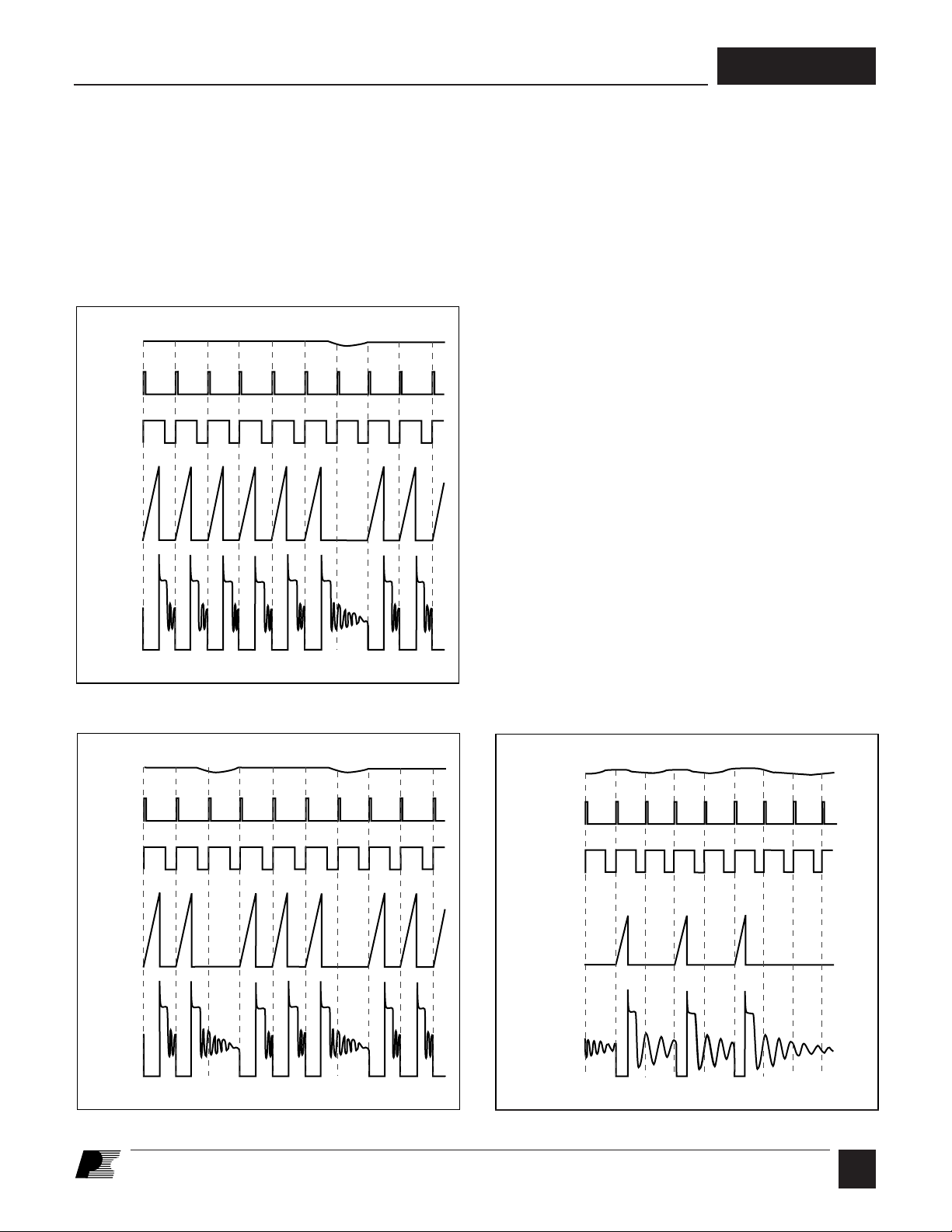
ON/OFF Operation with Current Limit State Machine
The internal clock of the TinySwitch-II runs all the time. At the
V
EN
CLOCK
D
MAX
I
DRAIN
V
DRAIN
PI-2749-050301
Figure 6. TinySwitch-II Operation at Near Maximum Loading.
beginning of each clock cycle, it samples the EN/UV pin to
decide whether or not to implement a switch cycle, and based
on the sequence of samples over multiple cycles, it determines
the appropriate current limit. At high loads, when the EN/UV
pin is high (less than 240 µA out of the pin), a switching cycle
with the full current limit occurs. At lighter loads, when EN/UV
is high, a switching cycle with a reduced current limit occurs.
At near maximum load, TinySwitch-II will conduct during
nearly all of its clock cycles (Figure 6). At slightly lower load,
it will “skip” additional cycles in order to maintain voltage
regulation at the power supply output (Figure 7). At medium
loads, cycles will be skipped and the current limit will be
reduced (Figure8). At very light loads, the current limit will be
reduced even further (Figure 9). Only a small percentage of
cycles will occur to satisfy the power consumption of the power
supply.
The response time of the TinySwitch-II ON/OFF control scheme
is very fast compared to normal PWM control. This provides
tight regulation and excellent transient response.
Power Up/Down
The TinySwitch-II requires only a 0.1 µF capacitor on the
BYPASS pin. Because of its small size, the time to charge this
capacitor is kept to an absolute minimum, typically 0.6 ms. Due
to the fast nature of the ON/OFF feedback, there is no overshoot
at the power supply output. When an external resistor (2 MΩ) is
connected from the positive DC input to the EN/UV pin, the power
MOSFET switching will be delayed during power-up
until the DC line voltage exceeds the threshold (100 V). Figures
10 and 11 show the power-up timing waveform of TinySwitch-II
V
EN
CLOCK
D
MAX
I
DRAIN
V
DRAIN
PI-2667-090700
Figure 7. TinySwitch-II Operation at Moderately Heavy Loading.
V
EN
CLOCK
D
MAX
I
DRAIN
V
DRAIN
Figure 8. TinySwitch-II Operation at Medium Loading.
PI-2377-091100
B
5
7/01
TNY264/266-268
PI-2381-1030801
0
12
Time (ms)
0
200
400
5
0
10
0
100
200
V
DC-INPUT
V
BYPASS
V
DRAIN
PI-2348-030801
0
.5 1
Time (s)
0
100
200
300
0
100
200
400
V
DC-INPUT
V
DRAIN
V
EN
CLOCK
D
MAX
I
DRAIN
V
DRAIN
PI-2661-072400
Figure 9. TinySwitch-II Operation at Very Light Load.
in applications with and without an external resistor (2 MΩ)
connected to the EN/UV pin.
During power-down, when an external resistor is used, the
power MOSFET will switch for 50 ms after the output loses
regulation. The power MOSFET will then remain off without
any glitches since the under-voltage function prohibits restart
when the line voltage is low.
Figure 12 illustrates a typical power-down timing waveform of
TinySwitch-II. Figure 13 illustrates a very slow power-down
timing waveform of TinySwitch-II as in standby applications.
The external resistor (2 MΩ) is connected to the EN/UV pin in
this case to prevent unwanted restarts.
200
V
100
DC-INPUT
0
Figure 11. TinySwitch-II Power-up without Optional External UV
Resistor Connected to EN/UV Pin.
Figure 12. Normal Power-down Timing (without UV).
200
PI-2383-030801
100
V
DC-INPUT
PI-2395-030801
10
V
5
0
400
200
0
Figure 10. TinySwitch-II Power-up with Optional External UV
6
BYPASS
V
DRAIN
0
12
Time (ms)
Resistor (2 MΩ) Connected to EN/UV Pin.
B
7/01
0
400
300
200
100
0
0
V
DRAIN
2.5 5
Time (s)
Figure 13. Slow Power-down Timing with Optional External
Ω
) UV Resistor Connected to EN/UV Pin.
(2 M
 Loading...