

Power Integrations TNY256Y, TNY256G, TNY256P Datasheet
TNY256
®
®
TinySwitch
Energy Efficient, Low Power Off-line Switcher
Plus
Product Highlights
TinySwitch Plus
• Extended power range
• Fully integrated auto-restart reduces short circuit current
• Line under-voltage sense eliminates turn-off glitches
• Frequency jittering dramatically reduces EMI (5 to 10 dB)
• TO-220 package option
Lowest Cost, Low Power Switcher Solution
• Lower cost than RCC, discrete PWM and other
integrated/hybrid solutions
• Cost effective replacement for bulky linear adapters
• Lowest component count
• Simple ON/OFF control – no loop compensation components
• No bias winding – simpler, lower cost transformer
• Designed to work with low cost external components
Extremely Energy Efficient
• Consumes only 30/60 mW at 115/230 VAC with no load
• Meets Blue Angel, Energy Star, Energy 2000 and
200mW European cell phone requirements for standby
• Saves $1 to $4 per year in energy costs (at $0.12/kWHr)
compared to bulky linear adapters
• Ideal for cellular phone chargers and adapters
High Performance at Low Cost
• High voltage powered – ideal for charger applications
• High bandwidth provides fast turn on with no overshoot
• Current limit operation rejects line frequency ripple
• Built-in current limit and thermal protection
Features
Description
The TNY256 extends the power range of the TinySwitch family
of energy efficient, low power off-line switchers. TinySwitch
devices use a breakthrough design to provide the lowest cost,
high efficiency, off-line switching solution for low power
applications. They integrate a 700 V power MOSFET, oscillator,
high voltage switched current source, current limit and thermal
shutdown circuitry into a single, monolithic device. The
devices start-up and operate on power derived from the DRAIN
voltage, eliminating the need for a transformer bias winding and
associated circuitry. TinySwitch's low operating current allows
power supply no-load consumption to be kept under 100 mW,
even at 265 VAC input.
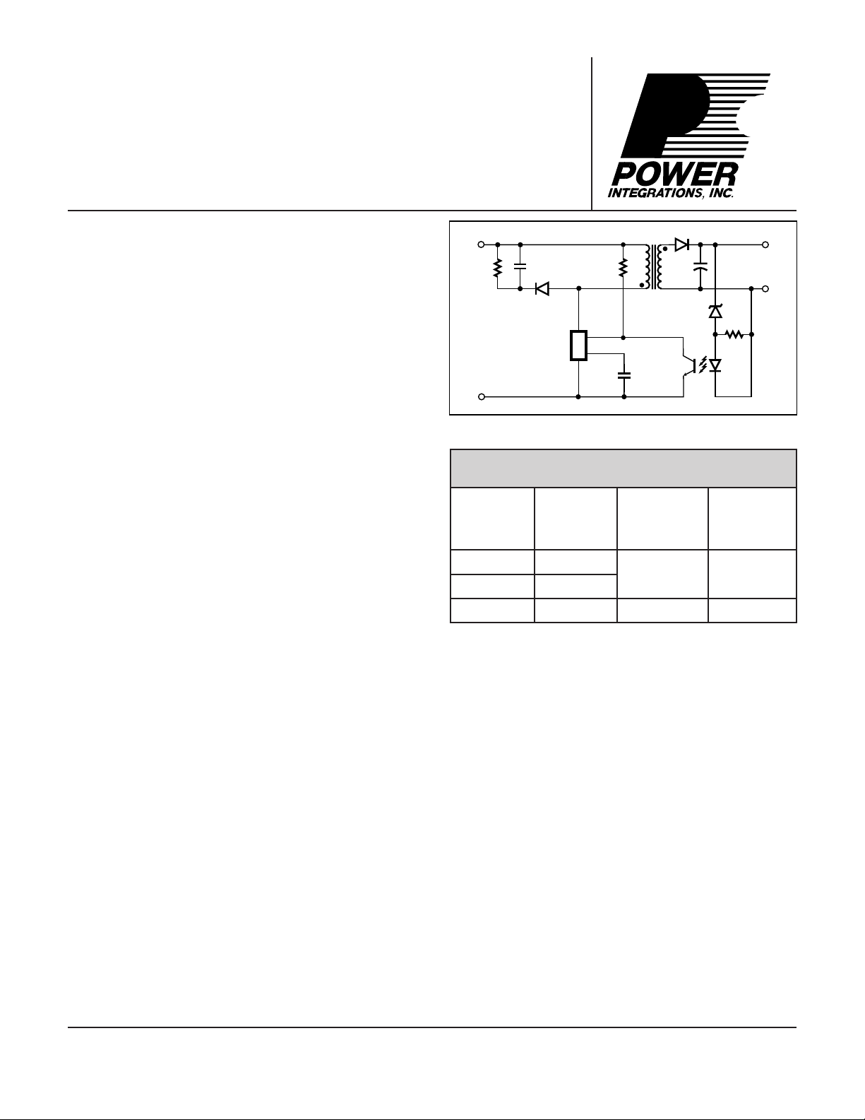
+
Optional
UV Resistor
Wide-Range
HV DC Input
TinySwitch Plus
–
Figure 1. Typical Standby Application.
D
EN/UV
BP
S
+
DC Output
–
PI-2363-022699
OUTPUT POWER CAPABILITY*
ORDER
PART
NUMBER
TNY256P
TNY256G
TNY256Y
Table 1. * The low end of the power ranges shown represent enclosed
adapters with minimal heat sinking whereas, the high end of the power
ranges represent open frame power supplies with adequate heat
sinking, both measured at an ambient of 50
Application Considerations section for more details.
The TinySwitch Plus incorporates auto-restart, line under-voltage
sense, and frequency jittering features. The auto-restart circuit
safely limits output power during fault conditions such as output
short or open loop. The auto-restart circuit is fully integrated and
does not require external timing components. The line undervoltage sense threshold can be externally programmed using a line
sense resistor. During start-up, this feature keeps the TNY256 off
until the input line voltage reaches the under-voltage threshold.
When the input line voltage is removed, the line under-voltage
circuit prevents auto-restart attempts after the output goes out of
regulation. This eliminates power down glitches caused by the
slow discharge of input storage capacitors present in applications
such as standby supplies. A single resistor is used to implement
this feature, eliminating what normally takes five to six components.
The line sense resistor is optional. The TNY256 operating frequency
of 130 kHz is jittered (frequency modulated) to reduce both quasipeak and average EMI, minimizing filtering costs.
PACKAGE
DIP-8
SMD-8
TO-220-7B
230 VAC or
115 VAC
w/Doubler
8-19 W
o
C. Please refer to the Key
85-265
VAC
5-10 W8-15 W
5-11 W
July 2001
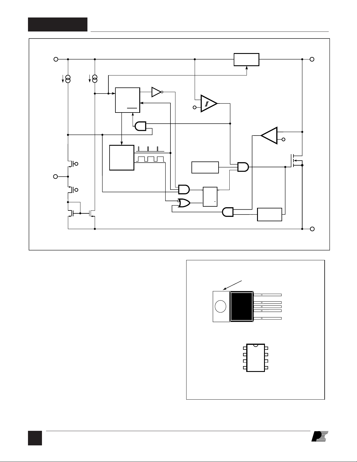
TNY256
BYPASS
(BP)
50 µA
ENABLE/
UNDER-VOLTAGE
(EN/UV)
1.5 V + V
1.5 V
DRAIN
REGULATOR
5.8 V
LINE UNDER-VOLTAGE
AUTORESTART
COUNTER
CLOCK
RESET
JITTER
CLOCK
TH
DC
MAX
OSCILLATOR
5.8 V
5.1 V
SHUTDOWN
+
-
THERMAL
SRQ
BYPASS PIN
UNDER-VOLTAGE
Q
LEADING
EDGE
BLANKING
+
-
V
I
LIMIT
(D)
Figure 2. Functional Block Diagram.
Pin Functional Description
DRAIN (D) Pin:
Power MOSFET drain connection. Provides internal operating
current for both start-up and steady-state operation.
BYPASS (BP) Pin:
Connection point for a 0.1 µF external bypass capacitor for the
internally generated 5.8 V supply.
ENABLE/UNDER-VOLTAGE (EN/UV) Pin:
This pin has dual functions, enable input and line under-voltage
sense. During normal operation, switching of the power
MOSFET is controlled by this pin. MOSFET switching is
terminated when a current greater than 50 µA is drawn out of
this pin. This pin also senses line under-voltage conditions
through an external resistor connected to the DC line voltage.
If there is no external resistor connected to this pin, TNY256
detects this and disables the line under-voltage function.
Tab Internally
Connected to SOURCE Pin
Y Package (TO-220-7B)
BP
S
S
EN/UV
P Package (DIP-8)
G Package (SMD-8)
Figure 3. Pin Configuration.
SOURCE
(S)
PI-2367-122398
7 D
5 NC
4 S
3 BP
1 EN/UV
1
2
3
4
8
S
7
S
6
S
5
D
PI-2500-031501
SOURCE (S) Pin:
Power MOSFET source connection. Primary return.
C
2
7/01
NO CONNECT (N) Pin
No connection.
TNY256
TinySwitch
Functional Description
TinySwitch combines a high voltage power MOSFET switch
with a power supply controller in one device. Unlike conventional
PWM (Pulse Width Modulator) controllers, TinySwitch uses a
simple ON/OFF control to regulate the output voltage.
The TNY256 controller consists of an Oscillator, Enable (Sense
and Logic) circuit, 5.8 V Regulator, Bypass pin Under-Voltage
circuit, Over Temperature Protection, Current Limit circuit,
Leading Edge Blanking and a 700 V power MOSFET. The
TNY256 incorporates additional circuitry for Line Under-Voltage
Sense, Auto-Restart and Frequency Jitter. Figure 2 shows the
functional block diagram with the most important features.
Oscillator
The typical oscillator frequency is internally set to an average of
130 kHz. Two signals are generated from the oscillator, the
Maximum Duty Cycle signal (DC
) and the Clock signal that
MAX
indicates the beginning of each cycle.
The TNY256 oscillator incorporates circuitry that introduces a
small amount of frequency jitter, typically 5 kHz peak-to-peak,
to minimize EMI emission. The modulation rate of the frequency
jitter (1 kHz) is set to optimize EMI reduction for both average
and quasi-peak emissions. The frequency jitter should be
measured with the oscilloscope triggered at the falling edge of
the DRAIN waveform. The waveform in Figure4 illustrates the
frequency jitter of the TNY256.
Enable Input Circuit
The enable input circuit at the EN/UV pin consists of a low
impedance source follower output set at 1.5 V. The current
through the source follower is limited to 50 µA with 10 µA of
hysteresis. When the current drawn out of the this pin exceeds
600
500
400
300
200
100
0
0
Figure 4. Frequency Jitter.
V
DRAIN
132.5 kHz
127.5 kHz
.5 1
Time (µs)
50 µA, a low logic level (disable) is generated at the output of
the enable circuit. This output is sampled at the beginning of
each cycle on the rising edge of the clock signal. If high, the
power MOSFET is turned on for that cycle (enabled), otherwise
the power MOSFET remains off (disabled). Since the sampling
is done only at the beginning of each cycle, subsequent
changes in the EN/UV pin voltage or current during the
remainder of the cycle are ignored.
Under most operating conditions (except when close to noload), the low impedance of the source follower, keeps the
voltage on the EN/UV pin from going much below 1.5 V, in the
disabled state. This improves the response time of the
optocoupler that is usually connected to this pin.
5.8 V Regulator
The 5.8 V regulator charges the bypass capacitor connected to
the BYPASS pin to 5.8 V by drawing a current from the voltage
on the DRAIN, whenever the MOSFET is off. The BYPASS
pin is the internal supply voltage node for the TinySwitch.
When the MOSFET is on, the TinySwitch runs off of the energy
stored in the bypass capacitor. Extremely low power
consumption of the internal circuitry allows the TinySwitch to
operate continuously from the current drawn from the DRAIN
pin. A bypass capacitor value of 0.1 µF is sufficient for both
high frequency de-coupling and energy storage.
BYPASS Pin Under-Voltage
The BYPASS pin under-voltage circuitry disables the power
MOSFET when the BYPASS pin voltage drops below 5.1 V.
Once the BYPASS pin voltage drops below 5.1 V, it must rise
back to 5.8 V to enable (turn-on) the power MOSFET.
Over Temperature Protection
The thermal shutdown circuitry senses the die temperature.
The threshold is set at 135 oC with 70 oC hysteresis. When the
die temperature rises above this threshold (135 oC) the power
MOSFET is disabled and remains disabled until the die
temperature falls by 70 oC, at which point it is re-enabled.
PI-2366-021299
Current Limit
The current limit circuit senses the current in the power
MOSFET. When this current exceeds the internal threshold
(I
), the power MOSFET is turned off for the remainder of
LIMIT
that cycle.
The leading edge blanking circuit inhibits the current limit
comparator for a short time (t
) after the power MOSFET is
LEB
turned on. This leading edge blanking time has been set so that
current spikes caused by primary-side capacitance and
secondary-side rectifier reverse recovery time will not cause
premature termination of the switching pulse.
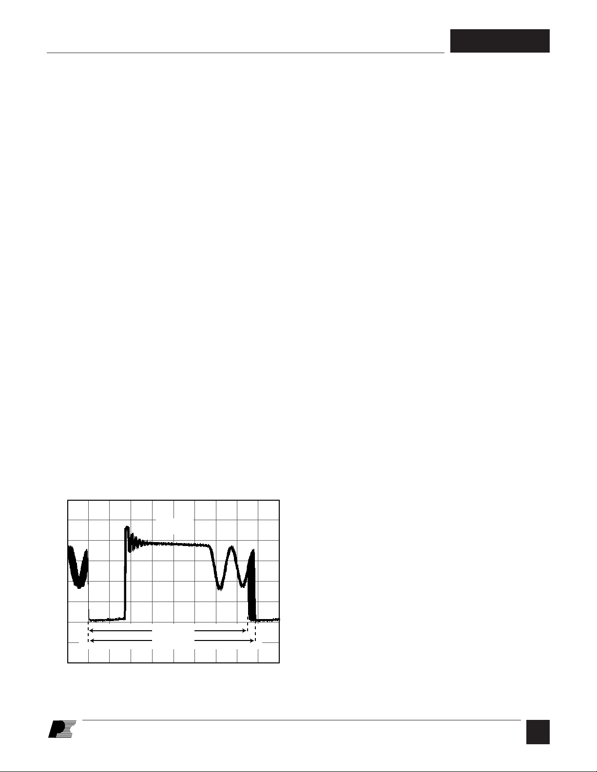
Auto-Restart
In the event of a fault condition such as output overload, output
7/01
C
3
TNY256
short, or an open loop condition, TNY256 enters into autorestart operation. An internal counter clocked by the oscillator
gets reset every time the EN/UV pin is pulled low. If the EN/
UV pin is not pulled low for 32 ms, the power MOSFET
switching is disabled for 128 ms (except in the case of line
under-voltage condition). The auto-restart alternately enables
and disables the switching of the power MOSFET until the fault
condition is removed. Figure 5 illustrates auto-restart circuit
operation in the presence of a temporary output short.
300
200
100
0
20
DRAIN
VOLTAGE
PI-2342-121198
In the event of line under-voltage condition, the switching of the
power MOSFET is disabled beyond its normal 128 ms time
until the line under-voltage condition goes away.
Line Under-Voltage (UVLO) Sense Circuit
The DC line voltage can be monitored by connecting an
external resistor from the DC line to the EN/UV pin. During
power-up or when the switching of the power MOSFET is
disabled in auto-restart, the current into the EN/UV pin must
exceed 50 µA to initiate switching of the power MOSFET.
During power-up, this is implemented by holding the BYPASS
pin to 5.1 V while the line under-voltage condition exists. The
BYPASS pin then rises from 5.1 V to 5.8V when the line undervoltage condition goes away. When the switching of the power
MOSFET is disabled in auto-restart mode and the line undervoltage condition exists, the counter is stopped. This stretches
the disable time beyond its normal 128ms until the line undervoltage condition goes away.
The line under-voltage circuit also detects when there is no
external resistor connected to the EN/UV pin. In this case the
line under-voltage function is disabled.
10
0
0
Time (ms)
Figure 5. TNY256 Auto-Restart Operation.
TinySwitch
Operation
OUTPUT
VOLTAGE
250 500
TinySwitch devices operate in the current limit mode. When
enabled, the oscillator turns the power MOSFET on at the
beginning of each cycle. The MOSFET is turned off when the
current ramps up to the current limit. The maximum on-time of
the MOSFET is limited to DC
by the oscillator. Since the
MAX
current limit and frequency of the TNY256 is constant, the
power delivered is proportional to the primary inductance of the
transformer and is relatively independent of the input voltage.
Therefore, the design of the power supply involves calculating
the primary inductance of the transformer for the maximum
power required. If the TNY256 is appropriately chosen for the
V
EN
CLOCK
D
MAX
I
DRAIN
V
DRAIN
Figure 6. TNY256 Operation at Heavy Load.
C
4
7/01
PI-2373-120998
V
EN
CLOCK
D
MAX
I
DRAIN
V
DRAIN
Figure 7. TNY256 Operation at Light Load.
PI-2377-120998
PI-2381-122398
0
12
Time (ms)
0
200
400
5
0
10
0
100
200
V
DC-BUS
V
BYPASS
V
DRAIN
200
TNY256
10
V
DC-BUS
0
V
5
0
0
BYPASS
V
DRAIN
0
Connected to EN/UV Pin.
12
Time (ms)
100
400
200
Figure 8. TNY256 Power-up With External Resistor (2 MΩ)
power level at the lowest input voltage, the calculated inductance
will ramp up the current to the current limit before the DC
limit is reached.
Enable Function
TNY256 senses the EN/UV pin to determine whether or not to
proceed with the next switch cycle as described earlier. Once
a cycle is started, it always completes the cycle (even when the
EN/UV pin changes state half way through the cycle). This
operation results in a power supply whose output voltage ripple
is determined by the output capacitor, amount of energy per
switch cycle and the delay of the feedback.
The EN/UV pin signal is generated on the secondary by
comparing the power supply output voltage with a reference
voltage. The EN/UV pin signal is high when the power supply
output voltage is less than the reference voltage.
In a typical implementation, the EN/UV pin is driven by an
optocoupler. The collector of the optocoupler transistor is
connected to the EN/UV pin and the emitter is connected to the
SOURCE pin. The optocoupler LED is connected in series with
a Zener across the DC output voltage to be regulated. When the
output voltage exceeds the target regulation voltage level
(optocoupler diode voltage drop plus Zener voltage), the
optocoupler diode will start to conduct, pulling the EN/UV pin
low. The Zener can be replaced by a TL431 device for
improved accuracy.
The EN/UV pin pull-down current threshold is nominally
50 µA, but is set to 40 µA the instant the threshold is exceeded.
This is reset back to 50 µA when the EN/UV pull-down current
drops below the current threshold of 40 µA.
PI-2383-122398
MAX
Figure 9. TNY256 Power-up Without External Resistor Connected
to EN/UV Pin.
ON/OFF Control
The internal clock of the TNY256 runs all the time. At the
beginning of each clock cycle, it samples the EN/UV pin to
decide whether or not to implement a switch cycle. If the
EN/UV pin is high (< 40 µA), then a switching cycle takes
place. If the EN/UV pin is low (greater than 50 µA) then no
switching cycle occurs, and the EN/UV pin status is sampled
again at the start of the subsequent clock cycle.
At full load, TNY256 will conduct during the majority of its
clock cycles (Figure6). At loads less than full load, it will
“skip” more cycles in order to maintain voltage regulation at the
secondary output. At light load or no load, almost all cycles will
be skipped (Figure7). A small percentage of cycles will
conduct to support the power consumption of the power supply.
The response time of the TNY256 ON/OFF control scheme is
very fast compared to normal PWM control. This provides tight
regulation and excellent transient response.
Power Up/Down
The TNY256 requires only a 0.1 µF capacitor on the BYPASS
pin. Because of the small size of this capacitor, the power-up
delay is kept to an absolute minimum, typically 0.3 ms. Due to
the fast nature of the ON/OFF feedback, there is no overshoot
at the power supply output. When an external resistor (2 MΩ)
is connected to the EN/UV pin, the power MOSFET switching
will be delayed during power-up until the DC line voltage
exceeds the threshold (100 V). Figures 8 and 9 illustrate the
power-up timing waveform of TNY256 in applications with
and without an external resistor (2 MΩ) connected to the
EN/UV pin.
7/01
C
5
TNY256
200
100
0
400
300
200
100
0
0
Time (s)
Figure 10. Normal Power-down Timing.
V
DC-BUS
V
DRAIN
.5 1
During power-down, when an external resistor is used, the
power MOSFET will switch for 32 ms after the output loses
regulation. The power MOSFET will then remain off without
any glitches since the under-voltage function prohibits restarts
when the line voltage is low.
Figure 10 illustrates a typical power-down timing waveform of
TNY256. Figure 11 illustrates a very slow power-down timing
waveform of TNY256 as in standby applications. The external
resistor (2 MΩ) is connected to the EN/UV pin in this case to
prevent restarts.
The TNY256 does not require a bias winding to provide power
to the chip, because it draws the power directly from the DRAIN
pin (see Functional Description above). This has two main
benefits. First, for a nominal application, this eliminates the
cost of an extra bias winding and associated components.
Secondly, for charger applications, the current-voltage
characteristic often allows the output voltage to fall to low
values while still delivering power. This type of application
normally requires a forward-bias winding which has many
more associated components, none of which are necessary with
the TNY256.
Current Limit Operation
Each switching cycle is terminated when the DRAIN current
reaches the current limit of the TNY256. For a given primary
inductance and input voltage, the duty cycle is constant.
However, the duty cycle does change inversely with the input
voltage providing “voltage feed-forward” advantages: good
line ripple rejection and relatively constant power delivery
independent of the input voltage.
BYPASS Pin Capacitor
The BYPASS pin uses a small 0.1 µF ceramic capacitor for
decoupling the internal power supply of the TNY256.
200
PI-2348-010599
100
0
400
300
200
100
0
0
Time (s)
Figure 11. Slow Power-down Timing with External (2 MΩ)
Resistor Connected to EN/UV Pin.
V
DC-BUS
V
DRAIN
2.5 5
Application Example
The TNY256 is ideal for low cost, high efficiency power
supplies in a wide range of applications such as PC standby,
cellular phone chargers, AC adapters, motor control, appliance
control and ISDN network termination. The 130kHz operation
allows the use of a low cost EE16 core transformer while still
providing good efficiency. The frequency jitter in TNY256
makes it possible to use a single inductor (or two small resistors
if lower efficiency is acceptable) in conjunction with two input
capacitors for input EMI filtering up to the 10W level. The
auto-restart function allows the design to be optimized for
maximum efficiency without consideration for short-circuit
current on the secondary. For applications requiring undervoltage lockout (UVLO), the TNY256 eliminates several
components and saves cost.
As an example, Figure12 shows a 9V, 0.6A, AC adapter
operating from a universal input range (85-265VAC). The AC
input is rectified and filtered by D1-D4, C1 and C2 to create a
high voltage DC bus which is connected to T1. Inductor L1
forms a pi-filter in conjunction with C1 and C2. The resistor R1
damps resonance in inductor L1. The frequency jitter in
TNY256 allows it to meet worldwide conducted EMI standards
using a simple pi-filter in combination with a small value
Y1-capacitor C5 and a shield winding between primary and
secondary windings inside transformer T1. Diode D5, capacitor
C3 and resistor R3 form an RCD clamp circuit that limits the
turn-off voltage spike to a safe value on the TNY256 DRAIN
pin.
The secondary winding is rectified and filtered by D6, C6 and
C7 to provide the 9V output. Additional filtering is provided
by L3 and C8. The output voltage is determined by the resistor
network R7 and R8. Resistor R9 maintains a bias current
PI-2395-010599
C
6
7/01
 Loading...