

Power Integrations TNY255P, TNY255G, TNY254P, TNY254G, TNY253G Datasheet
...
®
TNY253/254/255
®
TinySwitch
Energy Efficient, Low Power Off-line Switchers
Product Highlights
Family
Lowest Cost, Low Power Switcher Solution
• Lower cost than RCC, discrete PWM and other
integrated/hybrid solutions
• Cost effective replacement for bulky linear adapters
• Lowest component count
• Simple ON/OFF control – no loop compensation devices
• No bias winding – simpler, lower cost transformer
• Allows simple RC type EMI filter for up to 2 W from
universal input or 4 W from 115 VAC input
Extremely Energy Efficient
• Consumes only 30/60 mW at 115/230 VAC with no load
• Meets Blue Angel, Energy Star, Energy 2000 and
200mW European cell phone requirements for standby
• Saves $1 to $4 per year in energy costs (at $0.12/kWHr)
compared to bulky linear adapters
• Ideal for cellular phone chargers, standby power supplies
for PC, TV and VCR, utility meters, and cordless phones.
High Performance at Low Cost
• High voltage powered – ideal for charger applications
• Very high loop bandwidth provides excellent transient
response and fast turn on with practically no overshoot
• Current limit operation rejects line frequency ripple
• Glitch free output when input is removed
• Built-in current limit and thermal protection
• 44 kHz operation (TNY253/4) with snubber clamp
reduces EMI and video noise in TVs & VCRs
• Operates with optocoupler or bias winding feedback
+
Wide-Range
HV DC Input
–
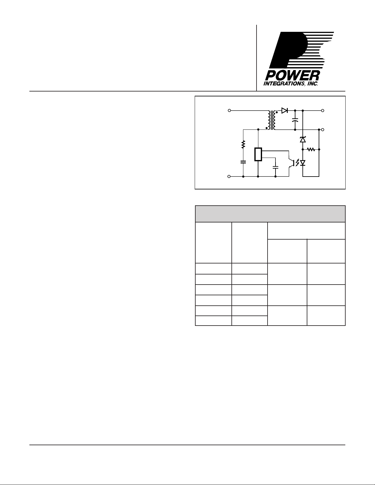
Figure 1. Typical Standby Application.
TinySwitch
ORDER
PART
NUMBER
TNY253P
TNY253G
TNY254P
TNY254G
TNY255P
TNY255G
PACKAGE
DIP-8
SMD-8
DIP-8
SMD-8
DIP-8
SMD-8
TinySwitch
D
EN
BP
S
SELECTION GUIDE
Recommended Range
for Lowest System Cost*
230 VAC or
115 VAC
w/Doubler
0-4 W
2-5 W
+
DC Output
–
PI-2178-022699
85-265
VAC
0-2 W
1-4 W
3.5-6.5 W4-10 W
Description
The TinySwitch family uses a breakthrough design to provide
the lowest cost, high efficiency, off-line switcher solution in the
0 to 10 W range. These devices integrate a 700 V power
MOSFET, oscillator, high voltage switched current source,
current limit and thermal shutdown circuitry. They start-up and
run on power derived from the DRAIN voltage, eliminating the
need for a transformer bias winding and the associated circuitry.
And yet, they consume only about 80 mW at no load, from
265VAC input. A simple ON/OFF control scheme also
eliminates the need for loop compensation.
The TNY253 and TNY254 switch at 44 kHz to minimize EMI
and to allow a simple snubber clamp to limit DRAIN spike
Table 1. *Please refer to the Key Application Considerations section
for details.
voltage. At the same time, they allow use of low cost EE16 core
transformers to deliver up to 5 W. The TNY253 is identical to
TNY254 except for its lower current limit, which reduces
output short circuit current for applications under 2.5W.
TNY255 uses higher switching rate of 130kHz to deliver up to
10 W from the same low cost EE16 core for applications such
as PC standby supply. An EE13 or EF13 core with safety
spaced bobbin can be used for applications under 2.5W.
Absence of a bias winding eliminates the need for taping/
margins in most applications, when triple insulated wire is used
for the secondary. This simplifies the transformer construction
and reduces cost.
July 2001
TNY253/254/255
S
Q
Q
BYPASS
ENABLE
50 µA
OSCILLATOR
1.5 V + V
TH
CLOCK
DC
MAX
5.8 V
5.1 V
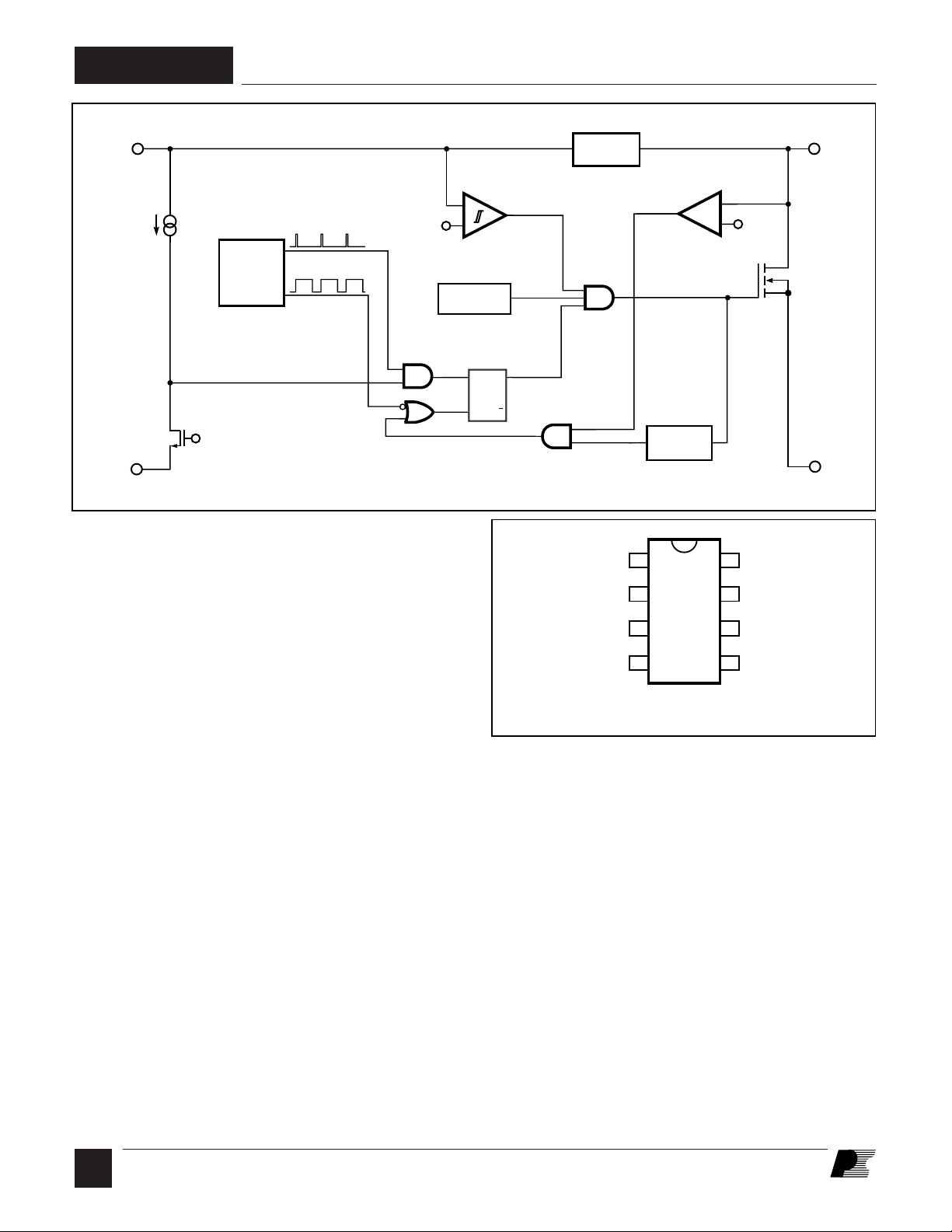
Figure 2. Functional Block Diagram.
Pin Functional Description
DRAIN (D) Pin:
Power MOSFET drain connection. Provides internal operating
current for both start-up and steady-state operation.
BYPASS (BP) Pin:
Connection point for an external bypass capacitor for the
internally generated 5.8V supply. Bypass pin is not intended
for sourcing supply current to external circuitry.
UNDER-VOLTAGE
+
-
THERMAL
SHUTDOWN
REGULATOR
5.8 V
BYPASS
SOURCE
SOURCE
ENABLE
1
2
3
4
P Package (DIP-8)
G Package (SMD-8)
Figure 3. Pin Configuration.
LEADING
EDGE
BLANKING
+
-
8
7
6
5
V
I
LIMIT
SOURCE
SOURCE
SOURCE
DRAIN
DRAIN
SOURCE
PI-2197-061898
PI-2199-031501
ENABLE (EN) Pin:
The power MOSFET switching can be terminated by pulling
this pin low. The I-V characteristic of this pin is equivalent to
a voltage source of approximately 1.5V with a source current
clamp of 50 µA.
SOURCE (S) Pin:
Power MOSFET source connection. Primary return.
TinySwitch
Functional Description
circuit, Hysteretic Over Temperature Protection, Current Limit
circuit, Leading Edge Blanking, and a 700V power MOSFET.
Figure 2 shows a functional block diagram with the most
important features.
Oscillator
The oscillator frequency is internally set at 44 kHz (130 kHz for
the TNY255). The two signals of interest are the Maximum
Duty Cycle signal (D
) which runs at typically 67% duty
MAX
cycle and the Clock signal that indicates the beginning of each
cycle. When cycles are skipped (see below), the oscillator
TinySwitch is intended for low power off-line applications. It
combines a high voltage power MOSFET switch with a power
supply controller in one device. Unlike a conventional PWM
frequency doubles (except for TNY255 which remains at
130kHz). This increases the sampling rate at the ENABLE pin
for faster loop response.
(Pulse Width Modulator) controller, the TinySwitch uses a
simple ON/OFF control to regulate the output voltage.
Enable (Sense and Logic)
The ENABLE pin circuit has a source follower input stage set
The TinySwitch controller consists of an Oscillator, Enable
(Sense and Logic) circuit, 5.8V Regulator, Under-Voltage
C
2
7/01
at 1.5V. The input current is clamped by a current source set
at 50 µA with 10 µA hysteresis. The output of the enable sense

TNY253/254/255
circuit is sampled at the rising edge of the oscillator Clock
signal (at the beginning of each cycle). If it is high, then the
power MOSFET is turned on (enabled) for that cycle, otherwise
the power MOSFET remains in the off state (cycle skipped).
Since the sampling is done only once at the beginning of each
cycle, any subsequent changes at the ENABLE pin during the
cycle are ignored.
5.8 V Regulator
The 5.8 V regulator charges the bypass capacitor connected to
the BYPASS pin to 5.8V by drawing a current from the voltage
on the DRAIN, whenever the MOSFET is off. The BYPASS
pin is the internal supply voltage node for the TinySwitch.
When the MOSFET is on, the TinySwitch runs off of the energy
stored in the bypass capacitor. Extremely low power
consumption of the internal circuitry allows the TinySwitch to
operate continuously from the current drawn from the DRAIN
pin. A bypass capacitor value of 0.1 µF is sufficient for both
high frequency de-coupling and energy storage.
Under Voltage
The under-voltage circuitry disables the power MOSFET when
the BYPASS pin voltage drops below 5.1V. Once the BYPASS
pin voltage drops below 5.1 V, it has to rise back to 5.8V to
enable (turn-on) the power MOSFET.
Hysteretic Over Temperature Protection
The thermal shutdown circuitry senses the die junction
temperature. The threshold is set at 135 °C with 70 °C hysteresis.
When the junction temperature rises above this threshold
(135 °C) the power MOSFET is disabled and remains disabled
until the die junction temperature falls by 70 °C, at which point
it is re-enabled.
Current Limit
The current limit circuit senses the current in the power
MOSFET. When this current exceeds the internal threshold
(I
), the power MOSFET is turned off for the remainder of
LIMIT
that cycle.
device are constant, the power delivered is proportional to the
primary inductance of the transformer and is relatively
independent of the input voltage. Therefore, the design of the
power supply involves calculating the primary inductance of
the transformer for the maximum power required. As long as
the TinySwitch device chosen is rated for the power level at the
lowest input voltage, the calculated inductance will ramp up the
current to the current limit before the DC
limit is reached.
MAX
Enable Function
The TinySwitch senses the ENABLE pin to determine whether
or not to proceed with the next switch cycle as described earlier.
Once a cycle is started TinySwitch always completes the cycle
(even when the ENABLE pin changes state half way through
the cycle). This operation results in a power supply whose
output voltage ripple is determined by the output capacitor,
amount of energy per switch cycle and the delay of the ENABLE
feedback.
The ENABLE signal is generated on the secondary by comparing
the power supply output voltage with a reference voltage. The
ENABLE signal is high when the power supply output voltage
is less than the reference voltage.
In a typical implementation, the ENABLE pin is driven by an
optocoupler. The collector of the optocoupler transistor is
connected to the ENABLE pin and the emitter is connected to
the SOURCE pin. The optocoupler LED is connected in series
with a Zener across the DC output voltage to be regulated.
When the output voltage exceeds the target regulation voltage
level (optocoupler diode voltage drop plus Zener voltage), the
optocoupler diode will start to conduct, pulling the ENABLE
pin low. The Zener could be replaced by a TL431 device for
improved accuracy.
The ENABLE pin pull-down current threshold is nominally
50 µA, but is set to 40 µA the instant the threshold is exceeded.
This is reset to 50 µA when the ENABLE pull-down current
drops below the current threshold of 40 µA.
The leading edge blanking circuit inhibits the current limit
comparator for a short time (t
) after the power MOSFET is
LEB
turned on. This leading edge blanking time has been set so that
current spikes caused by primary-side capacitance and
secondary-side rectifier reverse recovery time will not cause
premature termination of the switching pulse.
TinySwitch
Operation
TinySwitch is intended to operate in the current limit mode.
When enabled, the oscillator turns the power MOSFET on at
the beginning of each cycle. The MOSFET is turned off when
the current ramps up to the current limit. The maximum ontime of the MOSFET is limited to DC
by the oscillator.
MAX
Since the current limit and frequency of a given TinySwitch
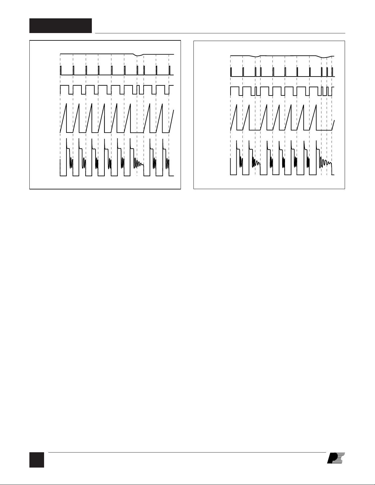
ON/OFF Control
The internal clock of the TinySwitch runs all the time. At the
beginning of each clock cycle the TinySwitch samples the
ENABLE pin to decide whether or not to implement a switch
cycle. If the ENABLE pin is high (< 40 µA), then a switching
cycle takes place. If the ENABLE pin is low (greater than
50 µA) then no switching cycle occurs, and the ENABLE pin
status is sampled again at the start of the subsequent clock cycle.
At full load TinySwitch will conduct during the majority of its
clock cycles (Figure 4). At loads less than full load, the
TinySwitch will “skip” more cycles in order to maintain voltage
regulation at the secondary output (Figure 5). At light load or
no load, almost all cycles will be skipped (Figure 6). A small
C
3
7/01
TNY253/254/255
V
EN
CLOCK
DC
MAX
I
DRAIN
V
DRAIN
PI-2255-061298
Figure 4. TinySwitch Operation at Heavy Load. Figure 5. TinySwitch Operation at Medium Load.
percentage of cycles will conduct to support the power
consumption of the power supply.
V
EN
CLOCK
DC
MAX
I
DRAIN
V
DRAIN
inductance and input voltage, the duty cycle is constant.
However, duty cycle does change inversely with the input
voltage providing “voltage feed-forward” advantages: good
The response time of TinySwitch ON/OFF control scheme is
very fast compared to normal PWM control. This provides high
line ripple rejection and relatively constant power delivery
independent of the input voltage.
line ripple rejection and excellent transient response.
44 kHz Switching Frequency (TNY253/254)
Power Up/Down
TinySwitch requires only a 0.1 µF capacitor on the BYPASS
pin. Because of the small size of this capacitor, the power-up
delay is kept to an absolute minimum, typically 0.3 ms (Figure7).
Due to the fast nature of the ON/OFF feedback, there is no
overshoot at the power supply output. During power-down, the
power MOSFET will switch until the rectified line voltage
drops to approximately 12 V. The power MOSFET will then
remain off without any glitches (Figure 8).
Switching frequency (with no cycle skipping) is set at 44kHz.
This provides several advantages. At higher switching
frequencies, the capacitive switching losses are a significant
proportion of the power losses in a power supply. At higher
frequencies, the preferred snubbing schemes are RCD or diode-
Zener clamps. However, due to the lower switching frequency
of TinySwitch , it is possible to use a simple RC snubber (and
even just a capacitor alone in 115VAC applications at powers
levels below 4W).
PI-2259-061298
Bias Winding Eliminated
TinySwitch does not require a bias winding to provide power to
the chip. Instead it draws the power directly from the DRAIN
pin (see Functional Description above). This has two main
benefits. First for a nominal application, this eliminates the cost
of an extra bias winding and associated components. Secondly,
for charger applications, the current-voltage characteristic often
allows the output voltage to fall to low values while still
delivering power. This type of application normally requires a
forward-bias winding which has many more associated
components, none of which are necessary with TinySwitch.
Current Limit Operation
Each switching cycle is terminated when the DRAIN current
reaches the current limit of the TinySwitch. For a given primary
C
4
7/01
Secondly, a low switching frequency also reduces EMI filtering
requirements. At 44kHz, the first, second and third harmonics
are all below 150kHz where the EMI limits are not very
restrictive. For power levels below 4W it is possible to meet
worldwide EMI requirements with only resistive and capacitive
filter elements (no inductors or chokes). This significantly
reduces EMI filter costs.
Finally, if the application requires stringent noise emissions
(such as video applications), then the TNY253/254 will allow
more effective use of diode snubbing (and other secondary
snubbing techniques). The lower switching frequency allows
RC snubbers to be used to reduce noise, without significantly
impacting the efficiency of the supply.
TNY253/254/255
V
EN
CLOCK
DC
MAX
I
DRAIN
V
DRAIN
PI-2261-061198
Figure 6. TinySwitch Operation at Light Load.
130 kHz Switching Frequency (TNY255)
The switching frequency (with no cycle skipping) is set at
130kHz. This allows the TNY255 to deliver 10W while still
using the same size, low cost transformer (EE16) as used by the
TNY253/254 for lower power applications.
BYPASS Pin Capacitor
The BYPASS pin uses a small 0.1 µF ceramic capacitor for
decoupling the internal power supply of the TinySwitch.
V
IN
V
DRAIN
0.2
Figure 7. TinySwitch Power-Up Timing Diagram.
V
IN
V
DRAIN
.4
Time (ms)
.6 .8
12 V
12 V
PI—2253-062398
0 V
0 V
1
PI—2251-062398
0 V
0 V
Application Examples
Television Standby
TinySwitch is an ideal solution for low cost, high efficiency
standby power supplies used in consumer electronic products
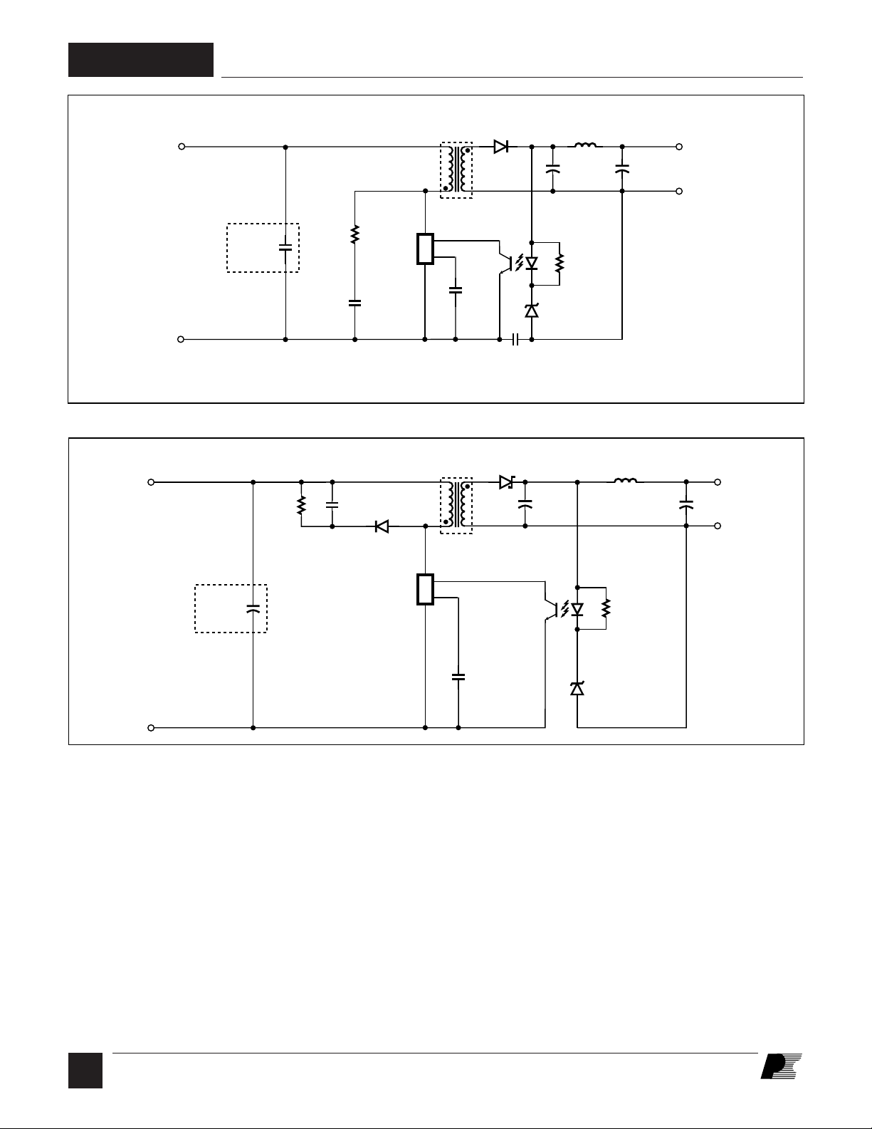
such as TVs. Figure9 shows a 7.5 V, 1.3 W flyback circuit that
uses TNY253 for implementing a TV standby supply. The
circuit operates from the DC high voltage already available
from the main power supply. This input voltage can range from
120 to 375VDC depending on the input AC voltage range that
the TV is rated for. Capacitor C1 filters the high voltage DC
supply, and is necessary only if there is a long trace length from
the source of the DC supply to the inputs of the TV standby
circuit. The high voltage DC bus is applied to the series
combination of the primary winding of T1 and the integrated
high voltage MOSFET inside the TNY253. The low operating
frequency of the TNY253 (44kHz), allows a low cost snubber
circuit C2 and R1 to be used in place of a primary clamp circuit.
In addition to limiting the DRAIN turn off voltage spike to a
safe value, the RC snubber also reduces radiated video noise by
0 100
Figure 8. TinySwitch Power Down Timing Diagram.
200
Time (ms)
300 400
500
lowering the dv/dt of the DRAIN waveform, which is critical for
video applications such as TV and VCR. On fixed frequency
PWM and RCC circuits, use of a snubber will result in an
undesirable fixed AC switching loss that is independent of load.
The ON/OFF control on the TinySwitch eliminates this problem
by scaling the effective switching frequency and therefore,
switching loss linearly with load. Thus the efficiency of the
supply stays relatively constant down to a fraction of a watt of
output loading.
The secondary winding is rectified and filtered by D1 and C4 to
create the 7.5V output. L1 and C5 provide additional filtering.
The output voltage is determined by the sum of the optocoupler
U2 LED forward drop (~ 1 V) and Zener diode VR1 voltage.
The resistor R2, maintains a bias current through the Zener to
improve its voltage tolerance.
C
5
7/01
TNY253/254/255
+
DC IN
120-375 VDC
Optional
C1
0.01 µF
1 kV
R1
100 Ω
1/2 W
C2
56 pF
1 kV
–
Figure 9. 1.3 W TV Stand-by Circuit using TNY253.
R1
150 kΩ
1 W
Optional
240-375
VDC
C1
0.01 µF
1 kV
TNY253P
C2
4700 pF
1 kV
1N4937
TNY255P
D1
U1
U1
T1
1
4
TinySwitch
D
EN
BP
S
0.1 µF
T1
1
4
TinySwitch
D
EN
BP
S
1N4934
10
8
C3
10
8
D1
C6
680 pF
Y1 Safety
D2
SB540
U2
LTV817
15 µH
330 µF
10 V
U2
SFH615-2
R2
1 kΩ
VR1
1N5235B
C4
2700 µF
6.3 V
C4
L1
L1
10 µH
R2
68 Ω
C5
47 µF
10 V
C5
220 µF
10 V
+ 7.5 V
RTN
PI-2246-082898
+ 5 V
RTN
Figure 10. 10 W PC Stand-by Supply Circuit.
PC Standby
The TNY255 was designed specifically for applications such as
PC standby, which require up to 10W of power from 230VAC
or 100/115VAC with doubler circuit. The TNY255 operates at
130kHz as opposed to 44kHz for TNY253/254. The higher
frequency operation allows the use of a low cost EE16 core
transformer up to the 10W level. Figure10 shows a 5V, 10W
circuit for such an application. The circuit operates from the
high voltage DC supply already available from the main power
supply. Capacitor C1 filters the high voltage DC supply, and is
necessary only if there is a long trace length from the source of
the DC supply to the inputs of the PC standby circuit. The high
voltage DC bus is applied to the primary winding of T1 in series
C
6
7/01
C3
0.1 µF
VR1
1N5229B
PI-2242-082898
with the integrated high voltage MOSFET inside the TNY255.
The diode D1, capacitor C2 and resistor R1 comprise the clamp
circuit that limits the turn-off voltage spike on the TinySwitch
DRAIN pin to a safe value. The secondary winding is rectified
and filtered by D2 and C4 to provide the 5V ouput. Additional
filtering is provided by L1 and C5. The output voltage is
determined by the sum of the optocoupler U2 LED forward
drop (~ 1V) and Zener diode VR1 voltage. The resistor R2,
maintains a bias current through the Zener to improve its
voltage tolerance.
Cellular Phone Charger
The TinySwitch is well suited for applications that require a
 Loading...