

Page 1
SCALE™-2+ 2SC0435T
SCALE™-2+ 2SC0435T
Preliminary Description & Application Manual
Dual-Channel High-power IGBT Driver
Abstract
The new SCALE™-2+ dual-driver core 2SC0435T combines unrivalled compactness with broad applicability.
The driver was designed for universal applications requiring high reliability. The 2SC0435T drives all usual
high-power IGBT modules up to 1700V. The embedded paralleling capability allows easy inverter design
covering higher power ratings. Multi-level topologies are also supported.
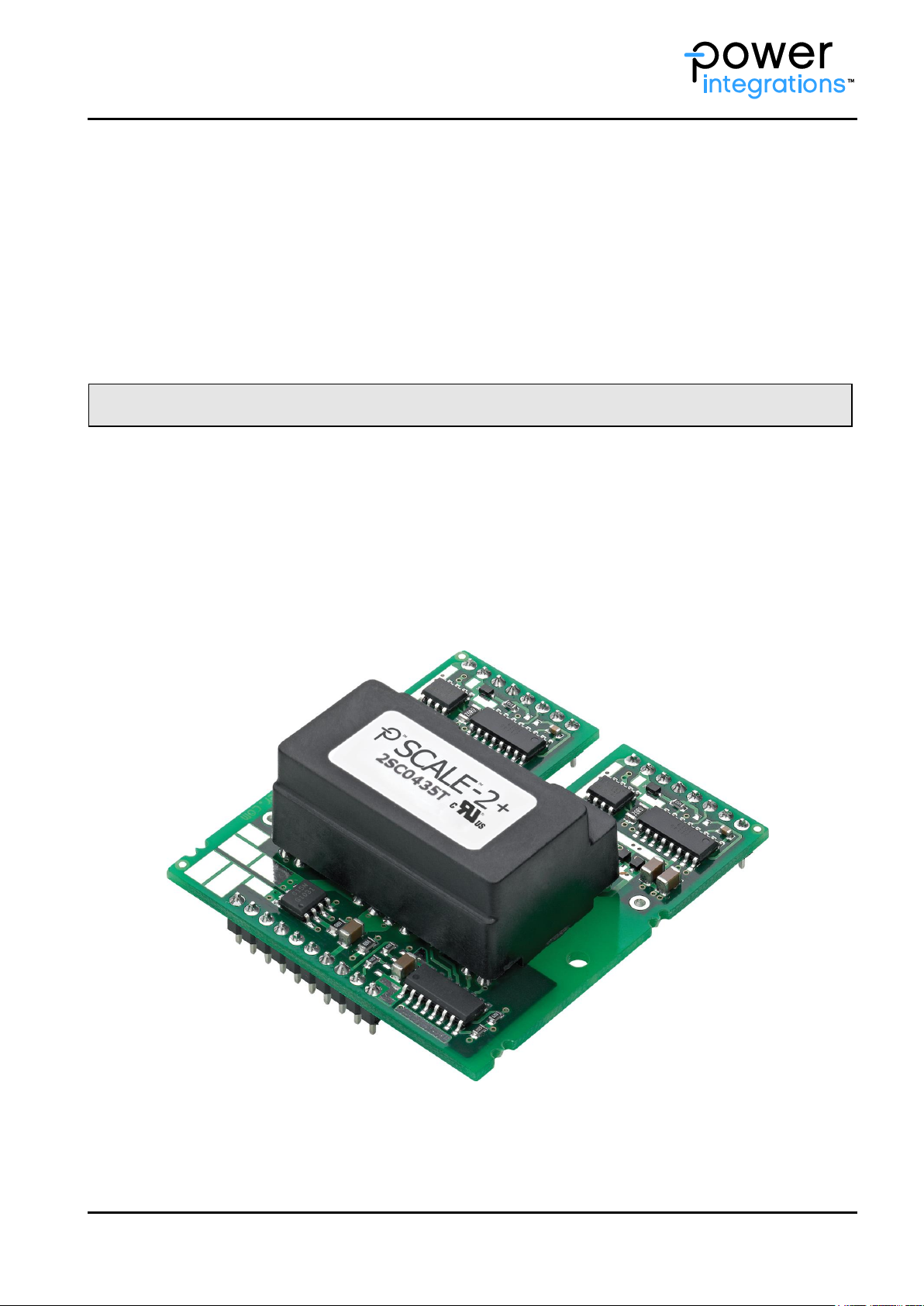
The 2SC0435T is the most compact driver core in its power range available for industrial applications, with a
footprint of only 57.2mm x 51.6mm and an insertion height of max. 20.5mm. It allows even the most
restricted insertion spaces to be efficiently used.
Fig. 1 2SC0435T driver core
www.power.com/igbt-driver Page 1
Page 2

SCALE™-2+ 2SC0435T
Preliminary Description & Application Manual
Contents
Abstract .......................................................................................................................................... 1
Contents ......................................................................................................................................... 2
Driver Overview ............................................................................................................................. 4
Mechanical Dimensions .................................................................................................................. 5
Pin Designation .............................................................................................................................. 7
Recommended Interface Circuitry for the Primary Side Connector .............................................. 8
Description of Primary Side Interface ........................................................................................... 8
General ............................................................................................................................... 8
VCC terminal ....................................................................................................................... 8
VDC terminal ....................................................................................................................... 9
MOD (mode selection) ......................................................................................................... 9
INA, INB (channel drive inputs, e.g. PWM) ........................................................................... 10
SO1, SO2 (status outputs) .................................................................................................. 10
TB (input for adjusting the blocking time Tb) ........................................................................ 10
Recommended Interface Circuitry for the Secondary Side Connectors ...................................... 11
Description of Secondary Side Interfaces .................................................................................... 11
General ............................................................................................................................. 11
DC/DC output (VISOx), emitter (VEx) and COMx terminals .................................................... 12
Reference terminal (REFx) .................................................................................................. 12
Collector sense (VCEx) ....................................................................................................... 12
Active clamping (ACLx) ...................................................................................................... 12
Gate turn-on (GHx) and turn-off (GLx) terminals .................................................................. 13
How Do 2SC0435T SCALE-2+ Drivers Work in Detail? ................................................................ 14
Power supply and electrical isolation ................................................................................... 14
Power-supply monitoring .................................................................................................... 14
VCE monitoring / short-circuit protection ............................................................................... 15
Desaturation protection with sense diodes ........................................................................... 16
Parallel connection of 2SC0435T ......................................................................................... 16
3-level or multilevel topologies ............................................................................................ 16
Additional application support for 2SC0435T ........................................................................ 16
Electrical Ratings for UL recognized types .................................................................................. 16
Bibliography ................................................................................................................................. 17
The Information Source: SCALE-2 and SCALE-2+ Driver Data Sheets ........................................ 17
Quite Special: Customized SCALE-2 and SCALE-2+ Drivers ........................................................ 17
www.power.com/igbt-driver Page 2
Page 3

SCALE™-2+ 2SC0435T
Preliminary Description & Application Manual
Technical Support ........................................................................................................................ 17
Quality .......................................................................................................................................... 17
Legal Disclaimer ........................................................................................................................... 18
Ordering Information ................................................................................................................... 19
Information about Other Products .............................................................................................. 19
Power Integrations Sales Offices ................................................................................................. 20
www.power.com/igbt-driver Page 3
Page 4
SCALE™-2+ 2SC0435T
Preliminary Description & Application Manual
Driver Overview
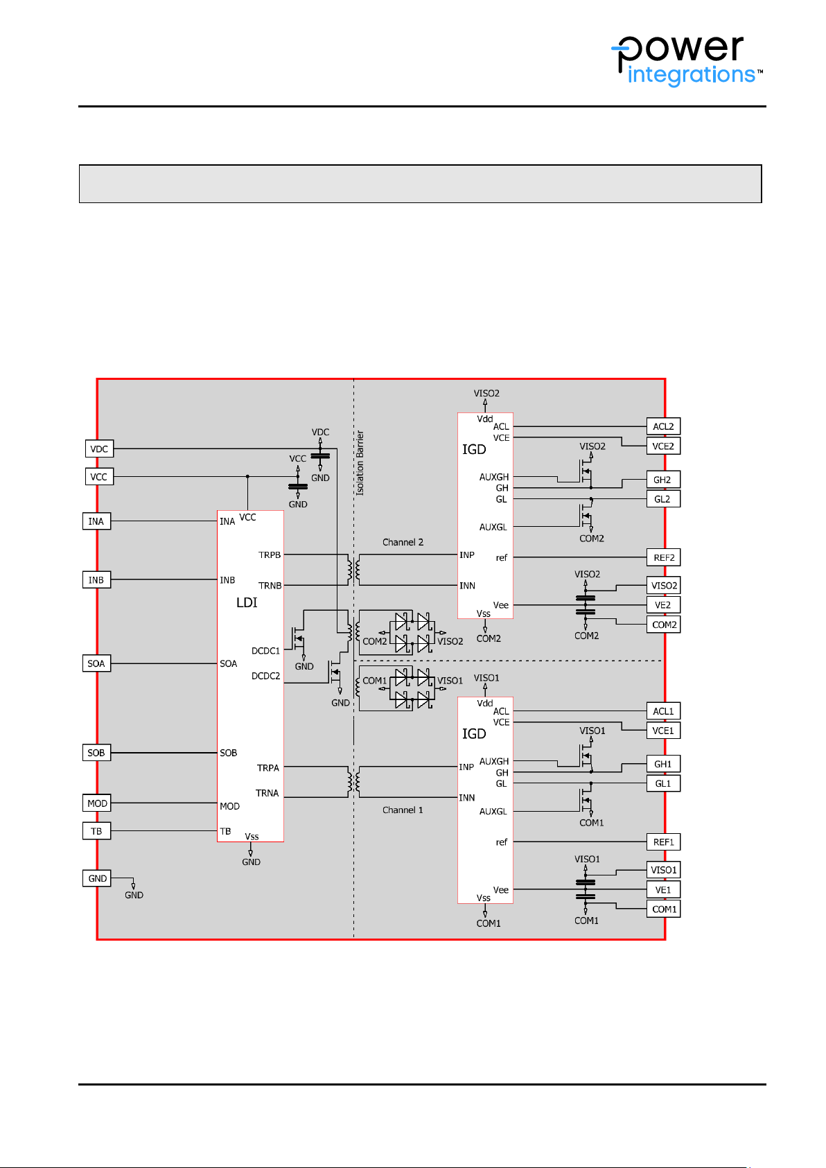
The 2SC0435T is a driver core equipped with Power Integrations' latest SCALE-2+ chipset /1/. The SCALE-2+
chipset is a set of application-specific integrated circuits (ASICs) that cover the main range of functions
needed to design intelligent gate drivers. The SCALE-2+ driver chipset is a further development of the proven
SCALE technology /2/.
The 2SC0435T targets medium-power, dual-channel IGBT and MOSFET applications. The driver supports
switching up to 100kHz at best-in-class efficiency. The 2SC0435T comprises a complete dual-channel IGBT
driver core, fully equipped with an isolated DC/DC converter, short-circuit protection, Advanced Active
Clamping (AAC) and supply-voltage monitoring.
9
Fig. 2 Block diagram of the driver core 2SC0435T
www.power.com/igbt-driver Page 4
Page 5

SCALE™-2+ 2SC0435T
Preliminary Description & Application Manual
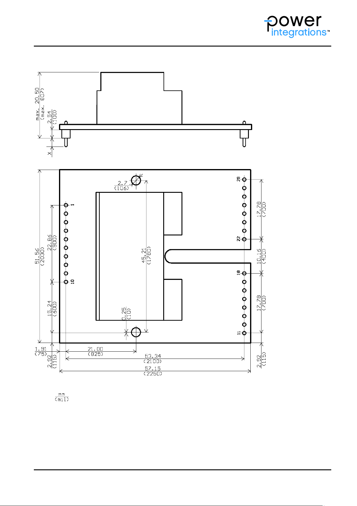
Mechanical Dimensions
Fig. 3 Interactive 3D drawing of 2SC0435T2H0-17
www.power.com/igbt-driver Page 5
Page 6
SCALE™-2+ 2SC0435T
X=2.54mm (100mil) for 2SC0435T2H0-17 and 2SC0435T2H0C-17
X=3.1mm (122mil) for 2SC0435T2G1-17 and 2SC0435T2G1C-17
X=5.84mm (230mil) for 2SC0435T2F1-17 and 2SC0435T2F1C-17
Preliminary Description & Application Manual
Fig. 4 Mechanical drawing of 2SC0435T
The primary side and secondary side pin grid is 2.54mm (100mil) with a pin cross section of
0.64mm x 0.64mm. Total outline dimensions of the board are 57.2mm x 51.6mm. The total height of the
driver is max. 20.5mm measured from the bottom of the pin bodies to the top of the populated PCB.
Recommended diameter of solder pads: Ø 2mm (79 mil)
Recommended diameter of drill holes: Ø 1mm (39 mil)
www.power.com/igbt-driver Page 6
Page 7

SCALE™-2+ 2SC0435T
Preliminary Description & Application Manual
Pin Designation
Pin No. and Name Function
Primary Side
1 VDC DC/DC converter supply
2 SO1 Status output channel 1; normally high-impedance, pulled down to low on fault
3 SO2 Status output channel 2; normally high-impedance, pulled down to low on fault
4 MOD Mode selection (direct/half-bridge mode)
5 TB Set blocking time
6 VCC Supply voltage; 15V supply for primary side
7 GND Ground
8 INA Signal input A; non-inverting input relative to GND
9 INB Signal input B; non-inverting input relative to GND
10 GND Ground
Secondary Sides
11 ACL1 Active clamping feedback channel 1; leave open if not used
12 VCE1 VCE sense channel 1; connect to IGBT collector through resistor network
13 REF1 Set VCE detection threshold channel 1; resistor to VE1
14 COM1 Secondary side ground channel 1
15 VE1 Emitter channel 1; connect to (auxiliary) emitter of power switch
16 VISO1 DC/DC output channel 1
17 GH1 Gate high channel 1; pulls gate high through turn-on resistor
18 GL1 Gate low channel 1; pulls gate low through turn-off resistor
19 Free
20 Free
21 Free
22 ACL2 Active clamping feedback channel 2; leave open if not used
23 VCE2 VCE sense channel 2; connect to IGBT collector through resistor network
24 REF2 Set VCE detection threshold channel 2; resistor to VE2
25 COM2 Secondary side ground channel 2
26 VE2 Emitter channel 2; connect to (auxiliary) emitter of power switch
27 VISO2 DC/DC output channel 2
28 GH2 Gate high channel 2; pulls gate high through turn-on resistor
29 GL2 Gate low channel 2; pulls gate low through turn-off resistor
Note: Pins with the designation “Free” are not physically present.
www.power.com/igbt-driver Page 7
Page 8
SCALE™-2+ 2SC0435T
Preliminary Description & Application Manual
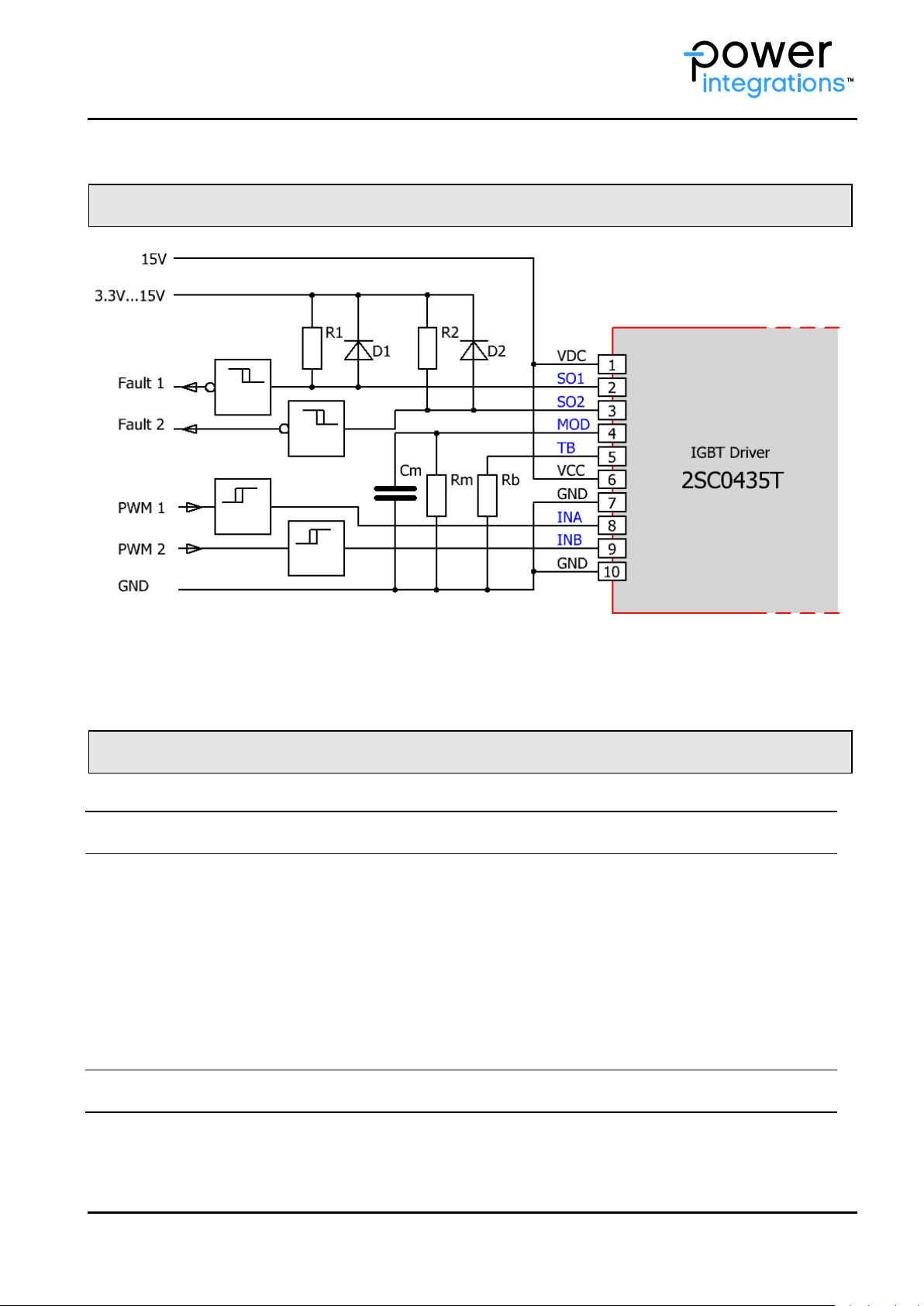
Recommended Interface Circuitry for the Primary Side Connector
Fig. 5 Recommended user interface of 2SC0435T (primary side)
Both ground pins must be connected together with low parasitic inductance. A common ground plane or wide
tracks are strongly recommended. The connecting distance between ground pins must be kept at a minimum.
Description of Primary Side Interface
General
The primary side interface of the driver 2SC0435T is very simple and easy to use.
The driver primary side is equipped with a 10-pin interface connector with the following terminals:
2 x power-supply terminals
2 x drive signal inputs
2 x status outputs (fault returns)
1 x mode selection input (half-bridge mode / direct mode)
1 x input to set the blocking time
All inputs and outputs are ESD-protected. Moreover, all digital inputs have Schmitt-trigger characteristics.
VCC terminal
The driver has one VCC terminal on the interface connector to supply the primary side electronics with 15V.
www.power.com/igbt-driver Page 8
Page 9
SCALE™-2+ 2SC0435T
Preliminary Description & Application Manual
VDC terminal
The driver has one VDC terminal on the interface connector to supply the DC-DC converters for the secondary
sides.
VDC should be supplied with 15V. It is recommended to connect the VCC and VDC terminals to a common 15V
power supply. In this case the driver limits the inrush current at startup and no external current limitation of
the voltage source for VDC is needed.
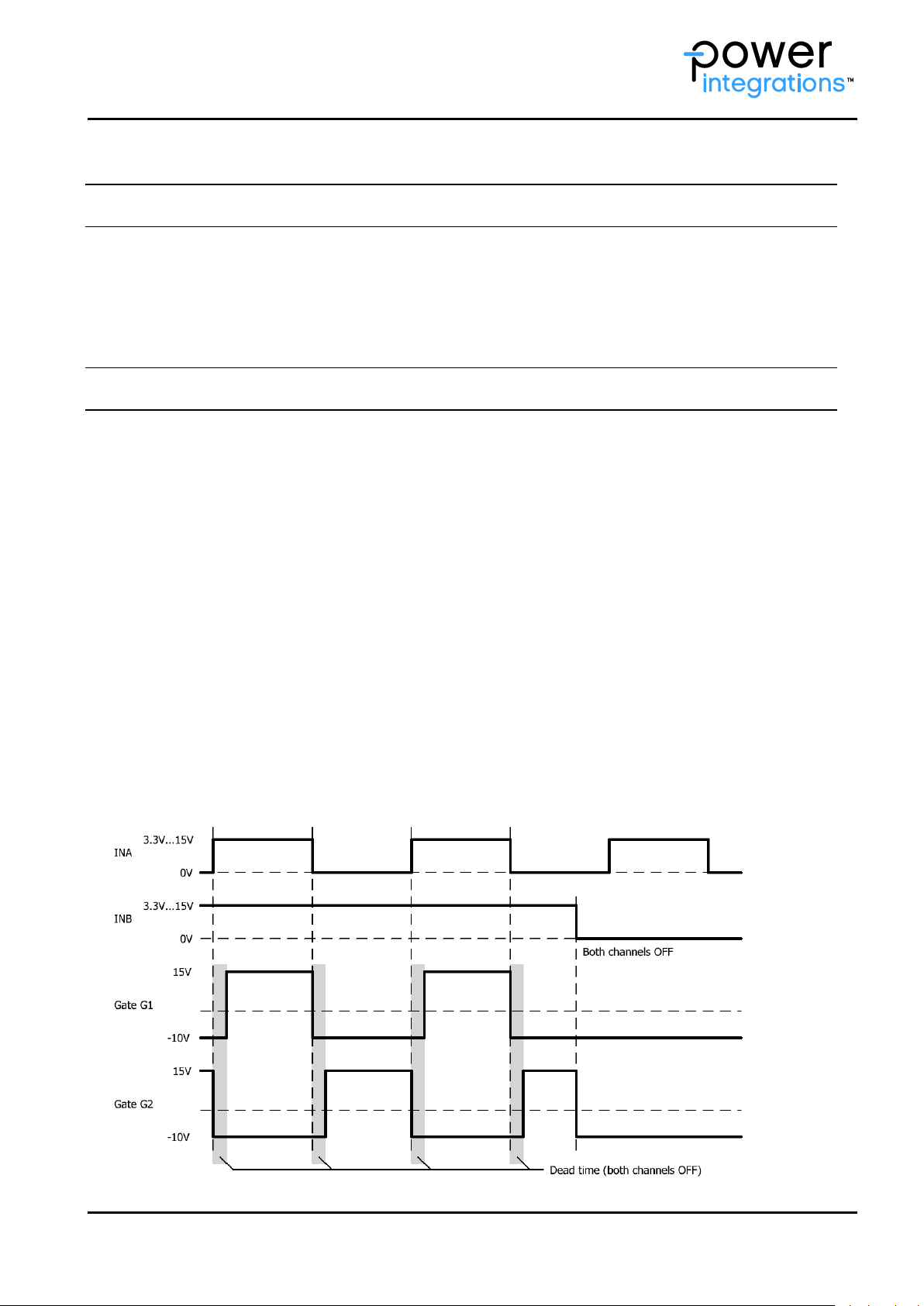
MOD (mode selection)
The MOD input allows the operating mode to be selected with a resistor connected to GND.
Direct mode
If the MOD input is connected to GND, direct mode is selected. In this mode, there is no interdependence
between the two channels. Input INA directly influences channel 1 while INB influences channel 2. High level
at an input (INA or INB) always results in turn-on of the corresponding IGBT. In a half-bridge topology, this
mode should be selected only when the dead times are generated by the control circuitry so that each IGBT
receives its own drive signal.
Caution: Synchronous or overlapping timing of both switches of a half-bridge basically shorts the DC-link.
Half-bridge mode
If the MOD input is connected to GND with a resistor 72k<Rm<181k, half-bridge mode is selected. In this
mode, the inputs INA and INB have the following functions: INA is the drive signal input while INB acts as the
enable input (Fig. 6). It is recommended to place a capacitor Cm=22nF in parallel to Rm in order to reduce the
deviation between the dead times at the rising and falling edges of INA respectively.
When input INB is low level, both channels are blocked. If it goes high, both channels are enabled and follow
the signal on the input INA. At the transition of INA from low to high, channel 2 turns off immediately and
channel 1 turns on after a dead time Td.
Fig. 6 Signals in half-bridge mode
www.power.com/igbt-driver Page 9
Page 10

SCALE™-2+ 2SC0435T
7.52][5.31][ sTkR
dm
51][0.1][ msTkR
bb
Preliminary Description & Application Manual
The value of the dead time Td is determined by the value of the resistor Rm according to the following formula
(typical value):
with 0.6μs<Td<4.1μs and 72kΩ<Rm<181kΩ
Note that the dead time may vary from sample to sample. A tolerance of approximately ±20% may be
expected. If higher timing precisions are required, Power Integrations recommends using the direct mode and
generating the dead time externally (refer to the Application Note AN-1101 /4/).
INA, INB (channel drive inputs, e.g. PWM)
INA and INB are basically drive inputs, but their function depends on the MOD input (see above). They safely
recognize signals in the whole logic-level range between 3.3V and 15V. Both input terminals feature Schmitttrigger characteristics (refer to the driver data sheet /3/). An input transition is triggered at any edge of an
incoming signal at INA or INB.
SO1, SO2 (status outputs)
The outputs SOx have open-drain transistors. When no fault condition is detected, the outputs have high
impedance. An internal current source of 500μA pulls the SOx outputs to a voltage of about 4V when leaved
open. When a fault condition (primary side supply undervoltage, secondary side supply undervoltage, IGBT
short-circuit or overcurrent) is detected, the corresponding status output SOx goes to low (connected to GND).
The diodes D1 and D2 must be Schottky diodes and must only be used when using 3.3V logic. For 5V…15V
logic, they can be omitted.
The maximum SOx current in a fault condition must not exceed the value specified in the driver data sheet
/3/.
Both SOx outputs can be connected together to provide a common fault signal (e.g. for one phase). However,
it is recommended to evaluate the status signals individually to allow fast and precise fault diagnosis.
How the status information is processed
a) A fault on the secondary side (detection of short-circuit of IGBT module or supply undervoltage) is
transmitted to the corresponding SOx output immediately. The SOx output is automatically reset
(returning to a high impedance state) after a blocking time Tb has elapsed (refer to “TB (input for
adjusting the blocking time Tb)” for timing information).
b) A supply undervoltage on the primary side is indicated to both SOx outputs at the same time. Both SOx
outputs are automatically reset (returning to a high impedance state) when the undervoltage on the
primary side disappears.
TB (input for adjusting the blocking time Tb)
The terminal TB allows the blocking time to be set by connecting a resistor Rb to GND (Fig. 5). The following
equation calculates the value of Rb connected between pins TB and GND in order to program the desired
blocking time Tb (typical value):
with 20ms<Tb<130ms and 71kΩ<Rb<181kΩ
The blocking time can also be set to a minimum of 9µs (typical) by selecting Rb=0Ω. The terminal TB must not
be left floating.
www.power.com/igbt-driver Page 10
Page 11
SCALE™-2+ 2SC0435T
02.1][02.0][ msTVV
bb
Preliminary Description & Application Manual
Note: It is also possible to apply a stabilized voltage at TB. The following equation is used to calculate the
voltage Vb between TB and GND in order to program the desired blocking time Tb (typical value):
with 20ms<Tb<130ms and 1.42<Vb<3.62V
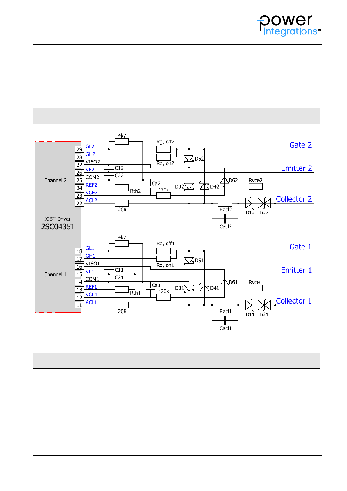
Recommended Interface Circuitry for the Secondary Side Connectors
Fig. 7 Recommended user interface of 2SC0435T with Advanced Active Clamping (secondary sides)
Description of Secondary Side Interfaces
General
Each driver’s secondary side (driver channel) is equipped with an 8-pin interface connector with the following
terminals (x stands for the number of the drive channel 1 or 2):
1 x DC/DC output terminal VISOx
1 x emitter terminal VEx
1 x reference terminal REFx for overcurrent or short-circuit protection
1x collector sense terminal VCEx
www.power.com/igbt-driver Page 11
Page 12

SCALE™-2+ 2SC0435T
Preliminary Description & Application Manual
1x active clamping terminal ACLx
1x turn-on gate terminals GHx
1x turn-off gate terminals GLx
All inputs and outputs are ESD-protected.
DC/DC output (VISOx), emitter (VEx) and COMx terminals
The driver is equipped with blocking capacitors on the secondary side of the DC/DC converter (for values,
refer to the data sheet /3/).
Power semiconductors with a gate charge of up to 3μC can be driven without additional capacitors on the
secondary side. For IGBTs or MOSFETs with a higher gate charge, a minimum value of 3µF external blocking
capacitance is recommended for every 1µC gate charge beyond 3µC. The blocking capacitors must be placed
between VISOx and VEx (C1x in Fig. 7) as well as between VEx and COMx (C2x in Fig. 7). They must be
connected as close as possible to the driver’s terminal pins with minimum inductance. It is recommended to
use the same capacitance value for both C1x and C2x. Ceramic capacitors with a dielectric strength >20V are
recommended.
If the capacitances C1x or C2x exceed 150µF, please contact Power Integrations' support service.
No static load must be applied between VISOx and VEx, or between VEx and COMx. A static load can be
applied between VISOx and COMx if necessary.
Reference terminal (REFx)
The reference terminal REFx allows the threshold to be set for short-circuit and/or overcurrent protection with
a resistor placed between REFx and VEx. A constant current of 150µA is provided at pin REFx.
Collector sense (VCEx)
The collector sense must be connected to the IGBT collector or MOSFET drain with the circuit shown in Fig. 7
in order to detect an IGBT or MOSFET overcurrent or short-circuit.
It is recommended to dimension the resistor value of R
flowing through R
1mA. It is possible to use a high-voltage resistor as well as series connected resistor. In any case, the
min. creepage distance related to the application must be considered.
The diode D
Schottky diodes must be explicitly avoided.
For more details about the functionality of this feature and the dimensioning of the response time, refer to
“VCE monitoring / short-circuit protection” on page 15.
must have a very low leakage current and a blocking voltage of >40V (e.g. BAS416).
6x
(e.g. 1.2-1.8MΩ for V
vcex
=1200V). The current through R
DC-LINK
in order to get a current of about 0.6-1mA
vcex
must not exceed
vcex
Active clamping (ACLx)
Active clamping is a technique designed to partially turn on the power semiconductor as soon as the collectoremitter (drain-source) voltage exceeds a predefined threshold. The power semiconductor is then kept in linear
operation.
Basic active clamping topologies implement a single feedback path from the IGBT’s collector through transient
voltage suppressor devices (TVS) to the IGBT gate. The 2SC0435T supports Power Integrations' Advanced
www.power.com/igbt-driver Page 12
Page 13

SCALE™-2+ 2SC0435T
Preliminary Description & Application Manual
Active Clamping, where the feedback is also provided to the driver’s secondary side at pin ACLx: as soon as
the voltage on the right side of the 20Ω resistor (Fig. 7) exceeds about 1.3V, the turn-off MOSFET is
progressively switched off in order to improve the effectiveness of the active clamping and to reduce the
losses in the TVS. The turn-off MOSFET is completely off when the voltage on the right side of the 20Ω
resistors (Fig. 7) approaches 20V (measured to COMx).
It is recommended to use the circuit shown in Fig. 7. The following parameters must be adapted to the
application:
TVS D
- Six 80V TVS with 600V IGBTs with DC-link voltages up to 430V. Good clamping results can be
- Six 150V TVS with 1200V IGBTs with DC-link voltages up to 800V. Good clamping results can be
- Six 220V TVS with 1700V IGBTs with DC-link voltages up to 1200V. Good clamping results can be
At least one bidirectional TVS (D2x) per channel must be used in order to avoid negative current
flowing through the TVS chain during turn-on of the antiparallel diode of the IGBT module due to its
forward recovery behavior. Such a current could, depending on the application, lead to undervoltage
of the driver secondary voltage VISOx to VEx (15V).
Note that it is possible to modify the number of TVS in a chain. The active clamping efficiency can be
improved by increasing the number of TVS used in a chain if the total threshold voltage remains at the
same value. Note also that the active clamping efficiency is highly dependent on the type of TVS used
(e.g. manufacturer).
R
the TVS and the IGBT to be optimized. It is recommended to determine the value with measurements
in the application. Typical values are: R
recommended to improve the effectiveness of active clamping.
, D2x. It is recommended to use:
1x
obtained with five unidirectional TVS P6SMBJ70A and one bidirectional TVS P6SMBJ70CA from
Semikron or with five unidirectional TVS SMBJ70A-E3 and one bidirectional TVS SMBJ70CA-E3 from
Vishay.
obtained with five unidirectional TVS SMBJ130A-E3 and one bidirectional TVS SMBJ130CA-E3 from
Vishay or five unidirectional TVS SMBJ130A-TR from ST and one bidirectional TVS P6SMBJ130CA
from Diotec.
obtained with five unidirectional TVS P6SMB220A and one bidirectional TVS P6SMB220CA from
Diotec or five unidirectional TVS SMBJ188A-E3 and one bidirectional TVS SMBJ188CA-E3 from
Vishay.
aclx
and C
: These parameters allow the effectiveness of the active clamping as well as the losses in
aclx
=0…150Ω and R
aclx
aclx*Caclx
=100ns…500ns. R
aclx
=0Ω is
D
Please note that the 20Ω resistor as well as diodes D3x, D4x and D5x must not be omitted if AAC is used. If AAC
is not used, the 20Ω resistor as well as diodes D3x and D4x can be omitted.
Application note AN-1302 /7/ gives information about Dynamic Advanced Active Clamping (DA2C) which allows
increasing the DC-link voltage to higher values in non-switching off-state condition.
, D4x and D5x: It is recommended to use Schottky diodes with blocking voltages >35V (>1A
3x
depending on the application).
Gate turn-on (GHx) and turn-off (GLx) terminals
These terminals allow the turn-on (GHx) and turn-off (GLx) gate resistors to be connected to the gate of the
power semiconductor. The GHx and GLx pins are available as separated terminals in order to set the turn-on
and turn-off resistors independently without the use of an additional diode. Please refer to the driver data
sheet /3/ for the limit values of the gate resistors used.
www.power.com/igbt-driver Page 13
Page 14

SCALE™-2+ 2SC0435T
Preliminary Description & Application Manual
A resistor between GLx and COMx of 4.7kΩ (other values are also possible) may be used in order to provide a
low-impedance path from the IGBT/MOSFET gate to the emitter/source even if the driver is not supplied with
power. No static load (e.g. resistors) must be placed between GLx and the emitter terminal VEx.
Note however that it is not advisable to operate the power semiconductors within a half-bridge with a driver in
the event of a low supply voltage. Otherwise, a high rate of increase of VCE may cause partial turn-on of these
IGBTs.
How Do 2SC0435T SCALE-2+ Drivers Work in Detail?
Power supply and electrical isolation
The driver is equipped with a DC/DC converter to provide an electrically insulated power supply to the gate
driver circuitry. All transformers (DC/DC and signal transformers) feature safe isolation to EN 50178,
protection class II between primary side and either secondary side.
Note that the driver requires a stabilized supply voltage.
Power-supply monitoring
The driver’s primary side as well as both secondary-side driver channels are equipped with a local
undervoltage monitoring circuit.
In the event of a primary-side supply undervoltage, the power semiconductors are driven with a negative gate
voltage to keep them in the off-state (the driver is blocked) and the fault is transmitted to both outputs SO1
and SO2 until the fault disappears.
In case of a secondary-side supply undervoltage, the corresponding power semiconductor is driven with a
negative gate voltage to keep it in the off-state (the channel is blocked) and a fault condition is transmitted to
the corresponding SOx output. The SOx output is automatically reset (returning to a high impedance state)
after the blocking time.
www.power.com/igbt-driver Page 14
Page 15
SCALE™-2+ 2SC0435T
Cax [pF]
R
thx
[kΩ]/V
thx
[V]
Response time [μs]
0
43 / 6.45
1.2
15
43 / 6.45
3.2
22
43 / 6.45
4.2
33
43 / 6.45
5.8
47
43 / 6.45
7.8 0 68 / 10.2
1.5
15
68 / 10.2
4.9
22
68 / 10.2
6.5
33
68 / 10.2
8.9
47
68 / 10.2
12.2
Fig. 8 Turn-on characteristic of an IGBT or
MOSFET
Preliminary Description & Application Manual
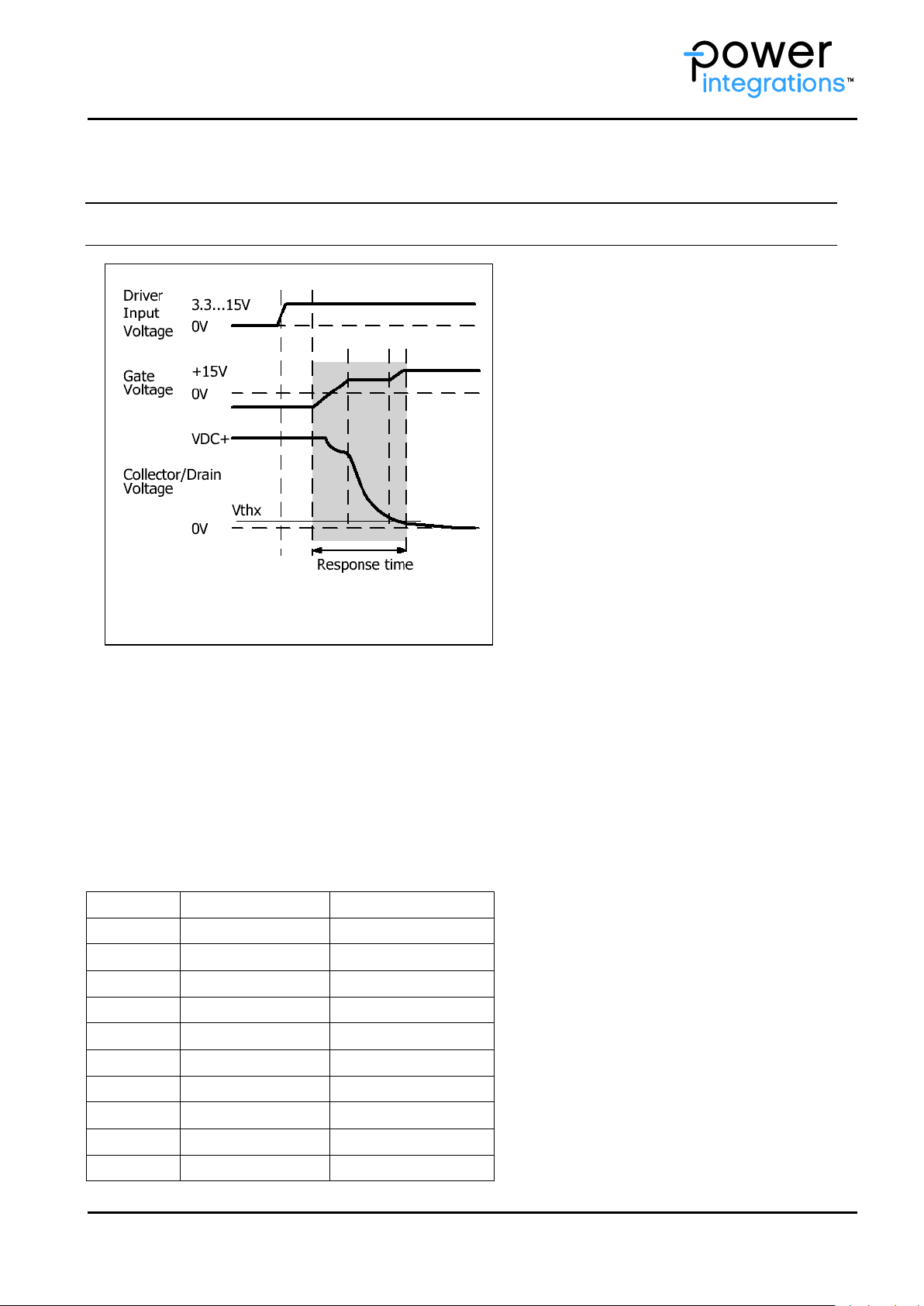
VCE monitoring / short-circuit protection
Each channel of the 2SC0435T driver is equipped
with a VCE monitoring circuit. The recommended
external circuitry is shown in Fig. 7. A resistor
(R
in Fig. 7) is used as the reference element
thx
for defining the turn-off threshold. The value of
the current through R
recommended to choose threshold levels of about
10V (R
driver will safely protect the IGBT against shortcircuit, but not necessarily against overcurrent.
Overcurrent protection has a lower timing priority
and is recommended to be realized within the
host controller.
In order to ensure that the 2SC0435T can be
applied as universally as possible, the response
time capacitor Cax is not integrated in the driver,
but must be connected externally.
values around 68kΩ). In this case the
thx
is 150μA (typical). It is
thx
During the response time, the VCE monitoring
circuit is inactive. The response time is the time
that elapses after turn-on of the power
semiconductor until the collector/drain voltage is measured (Fig. 8).
Both IGBT collector-emitter voltages are measured individually. VCE is checked after the response time at turnon to detect a short circuit or overcurrent. If the measured VCE at the end of the response time is higher than
the programmed threshold V
the corresponding power semiconductor. The fault status is immediately transferred to the corresponding SOx
output of the affected channel. The power semiconductor is kept in off-state (non-conducting) and the fault is
shown at pin SOx as long as the blocking time Tb is active.
The blocking time Tb is applied independently to each channel. Tb starts as soon as VCE exceeds the threshold
of the VCE monitoring circuit outside the response time span.
The value of the response time capacitors Cax can be determined with the following table in order to set the
desired response time (R
, the driver detects a short circuit or overcurrent. The driver then switches off
thx
=1.8MΩ, DC-link voltage V
vcex
DC-LINK
>550V):
Table 1 Typical response time in function of the capacitance Cax and the resistance R
www.power.com/igbt-driver Page 15
thx
Page 16
SCALE™-2+ 2SC0435T
Power/Channel
Gate Current
Control Circuit
(Input/Output)
System Voltage
4W
35A
15Vdc
730Vac/dc
Preliminary Description & Application Manual
As the parasitic capacitances on the host PCB may influence the response time it is recommended to measure
it in the final design. It is important to define a response time which is smaller than the max. allowed shortcircuit duration of the used power semiconductor.
Note that the response time increases at DC-link voltage values lower than 550V and/or higher threshold
voltage values V
Desaturation protection with sense diodes
If desaturation protection with sense diodes is required with 2SC0435T, please refer to the application note
AN-1101 /4/.
Parallel connection of 2SC0435T
If parallel connection of 2SC0435T drivers is required, please refer to the application note
AN-0904 /5/.
. The response time will decrease at lower threshold voltage values.
thx
3-level or multilevel topologies
If 2SC0435T drivers are to be used in 3-level or multilevel topologies, please refer to the application note
AN-0901 /6/.
Additional application support for 2SC0435T
For additional application support using 2SC0435T drivers, please refer to the application note AN-1101 /4/.
Electrical Ratings for UL recognized types
The following ratings apply for the UL recognized product versions according to the UL definitions:
www.power.com/igbt-driver Page 16
Page 17
SCALE™-2+ 2SC0435T
Preliminary Description & Application Manual
Bibliography
/1/ Paper: Smart Power Chip Tuning, Bodo’s Power Systems, May 2007
/2/ “Description and Application Manual for SCALE™ Drivers”, Power Integrations
/3/ Data sheet SCALE™-2+ driver core 2SC0435T, Power Integrations
/4/ Application note AN-1101: Application with SCALE™-2 and SCALE™-2+ Gate Driver Cores, Power
Integrations
/5/ Application note AN-0904: Direct Paralleling of SCALE™-2 Gate Driver Cores, Power Integrations
/6/ Application note AN-0901: Methodology for Controlling Multi-Level Converter Topologies with
SCALE™-2 IGBT Drivers, Power Integrations
/7/ Application note AN-1302: Dynamic Advanced Active Clamping (DA2C), Power Integrations
Note: The Application Notes are available on the Internet at www.power.com/igbt-driver/go/app-note and
the papers at www.power.com/igbt-driver/go/papers.
The Information Source: SCALE-2 and SCALE-2+ Driver Data Sheets
Power Integrations offers the widest selection of gate drivers for power MOSFETs and IGBTs for almost any
application requirements. The largest website on gate-drive circuitry anywhere contains all data sheets,
application notes and manuals, technical information and support sections: www.power.com.
Quite Special: Customized SCALE-2 and SCALE-2+ Drivers
If you need an IGBT driver that is not included in the delivery range, please don’t hesitate to contact Power
Integrations or your Power Integrations sales partner.
Power Integrations has more than 30 years experience in the development and manufacture of intelligent gate
drivers for power MOSFETs and IGBTs and has already implemented a large number of customized solutions.
Technical Support
Power Integrations provides expert help with your questions and problems:
www.power.com/igbt-driver/go/support
Quality
The obligation to high quality is one of the central features laid down in the mission statement of Power
Integrations Switzerland GmbH. Our quality management system assures state-of-the-art processes
throughout all functions of the company, certified by ISO9001 standards.
www.power.com/igbt-driver Page 17
Page 18

SCALE™-2+ 2SC0435T
Preliminary Description & Application Manual
Legal Disclaimer
The statements, technical information and recommendations contained herein are believed to be accurate as
of the date hereof. All parameters, numbers, values and other technical data included in the technical
information were calculated and determined to our best knowledge in accordance with the relevant technical
norms (if any). They may base on assumptions or operational conditions that do not necessarily apply in
general. We exclude any representation or warranty, express or implied, in relation to the accuracy or
completeness of the statements, technical information and recommendations contained herein. No
responsibility is accepted for the accuracy or sufficiency of any of the statements, technical information,
recommendations or opinions communicated and any liability for any direct, indirect or consequential loss or
damage suffered by any person arising therefrom is expressly disclaimed.
www.power.com/igbt-driver Page 18
Page 19

SCALE™-2+ 2SC0435T
Preliminary Description & Application Manual
Ordering Information
Our international terms and conditions of sale apply.
Type Designation Description
2SC0435T2F1-17 Dual-channel SCALE-2+ driver core (Lead free, connector pin length: 5.84mm,
increased EMI capability)
2SC0435T2F1C-17 Dual-channel SCALE-2+ driver core (Lead free, connector pin length: 5.84mm,
increased EMI capability, conformal coating)
2SC0435T2G1-17 Dual-channel SCALE-2+ driver core (Lead free, connector pin length: 3.1mm,
increased EMI capability)
2SC0435T2G1C-17 Dual-channel SCALE-2+ driver core (Lead free, connector pin length: 3.1mm,
increased EMI capability, conformal coating)
2SC0435T2H0-17 Dual-channel SCALE-2+ driver core (Lead free, connector pin length: 2.54mm,
increased EMI capability)
2SC0435T2H0C-17 Dual-channel SCALE-2+ driver core (Lead free, connector pin length: 2.54mm,
increased EMI capability, conformal coating)
Product home page: www.power.com/igbt-driver/go/2SC0435T
Refer to www.power.com/igbt-driver/go/nomenclature for information on driver nomenclature
Information about Other Products
For other driver cores:
Direct link: www.power.com/igbt-driver/go/cores
For other drivers, product documentation, evaluation systems and application support
Please click onto: www.power.com
2009…2018 Power Integrations Switzerland GmbH. All rights reserved.
We reserve the right to make any technical modifications without prior notice. Version 2.7 from 2018-02-05
www.power.com/igbt-driver Page 19
Page 20

SCALE™-2+ 2SC0435T
WORLD HEADQUARTERS
5245 Hellyer Avenue
San Jose, CA 95138 USA
Tel: +1-408-414-9200
Fax: +1-408-414-9765
Email: usasales@power.com
AMERICAS EAST
7360 McGinnis Ferry Road
Suite 225
Suwannee, GA 30024 USA
Tel: +1-678-957-0724
Fax: +1-678-957-0784
Email: usasales@power.com
AMERICAS CENTRAL
333 Sheridan Road
Winnetka, IL 60093 USA
Tel: +1-847-721-6293
Email: usasales@power.com
AMERICAS WEST
5245 Hellyer Avenue
San Jose, CA 95138 USA
Tel: +1-408-414-8778
Fax: +1-408-414-3760
Email: usasales@power.com
CHINA (Shanghai)
Room 2410, Charity Plaza
No. 88 North Caoxi Road
Shanghai, 200030 China
Tel: +86-21-6354-6323
Fax: +86-21-6354-6325
Email: chinasales@power.com
CHINA (Shenzhen)
17/F, Hivac Building, No 2
Keji South 8th Road, Nanshan District
Shenzhen, 518057 China
Tel: +86-755-8672-8689
Fax: +86-755-8672-8690
Email: chinasales@power.com
GERMANY (AC-DC/LED Sales)
Lindwurmstrasse 114
80337 München, Germany
Tel: +49-89-5527-39100
Fax: +49-89-1228-5374
Email: eurosales@power.com
GERMANY (Gate Driver Sales)
HellwegForum 1
59469 Ense, Germany
Tel: +49-2938-64-39990
Email: igbt-driver.sales@power.com
INDIA (Bangalore)
#1, 14th Main Road
Vasanthangar
Bangalore, 560052 India
Tel 1: +91-80-4113-8020
Tel 2: +91-80-4113-8028
Fax: +91-80-4113-8023
Email: indiasales@power.com
INDIA (Mumbai)
Unit: 106-107, Sagar Tech Plaza-B
Sakinaka, Andheri Kurla Road
Mumbai, Maharashtra 400072 India
Tel 1: +91-22-4003-3700
Tel 2: +91-22-4003-3600
Email: indiasales@power.com
INDIA (New Dehli)
#45, Top Floor
Okhla Industrial Area, Phase - III
New Dehli, 110020 India
Tel 1: +91-11-4055-2351
Tel 2: +91-11-4055-2353
Email: indiasales@power.com
ITALY
Via Milanese 20
20099 Sesto San Giovanni (MI), Italy
Tel: +39-02-4550-8708
Email: eurosales@power.com
JAPAN
Kosei Dai-3 Bldg.
2-12-11, Shin-Yokohama, Kohoku-ku
Yokohama-shi, Kanagawa
Japan 222-0033
Tel: +81-45-471-1021
Fax: +81-45-471-3717
Email: japansales@power.com
KOREA
RM602, 6FL, 22
Teheran-ro 87-gil, Gangnam-gu
Seoul, 06164 Korea
Tel: +82-2-2016-6610
Fax: +82-2-2016-6630
Email: koreasales@power.com
SINGAPORE
51 Newton Road
#19-01/05 Goldhill Plaza
Singapore, 308900
Tel 1: +65-6358-2160
Tel 2: +65-6358-4480
Fax: +65-6358-2015
Email: singaporesales@power.com
TAIWAN
5F, No. 318, Nei Hu Rd., Sec. 1
Nei Hu Dist.
Taipei, 114 Taiwan
Tel: +886-2-2659-4570
Fax: +886-2-2659-4550
Email: taiwansales@power.com
UNITED KINGDOM
Bulding 5, Suite 21
The Westbrook Centre
Milton Road
Cambridge, CB4 1YG United Kingdom
Tel: +44-7823-557-484
Email: eurosales@power.com
Preliminary Description & Application Manual
Power Integrations Sales Offices
www.power.com/igbt-driver Page 20
 Loading...