

Page 1
SCALE™-2 1SC0450E2B0
SCALE™-2 1SC0450E2B0
Preliminary Description & Application Manual
Single-Channel Cost-Effective Driver Core for IGBTs up to 4500V and 6500V
Abstract
The 1SC0450E2B0 single-channel SCALE™-2 driver core combines unrivalled compactness with broad
applicability and cost-effectiveness. It is designed for industrial and traction applications requiring high
reliability. The 1SC0450E2B0 drives all usual high-voltage IGBT modules up to 4500V and 6500V. Up to four
parallel-connected IGBT modules can be driven to cover higher power ratings. Multi-level topologies
involving 3300V or 4500V IGBTs with higher isolation requirements can also be easily supported by the
1SC0450E2B0.
The 1SC0450E2B0 supports maximal design flexibility as no fiber-optic links are assembled on the driver
board. Gate drive input and output signals are provided over dedicated electrical interface connectors.
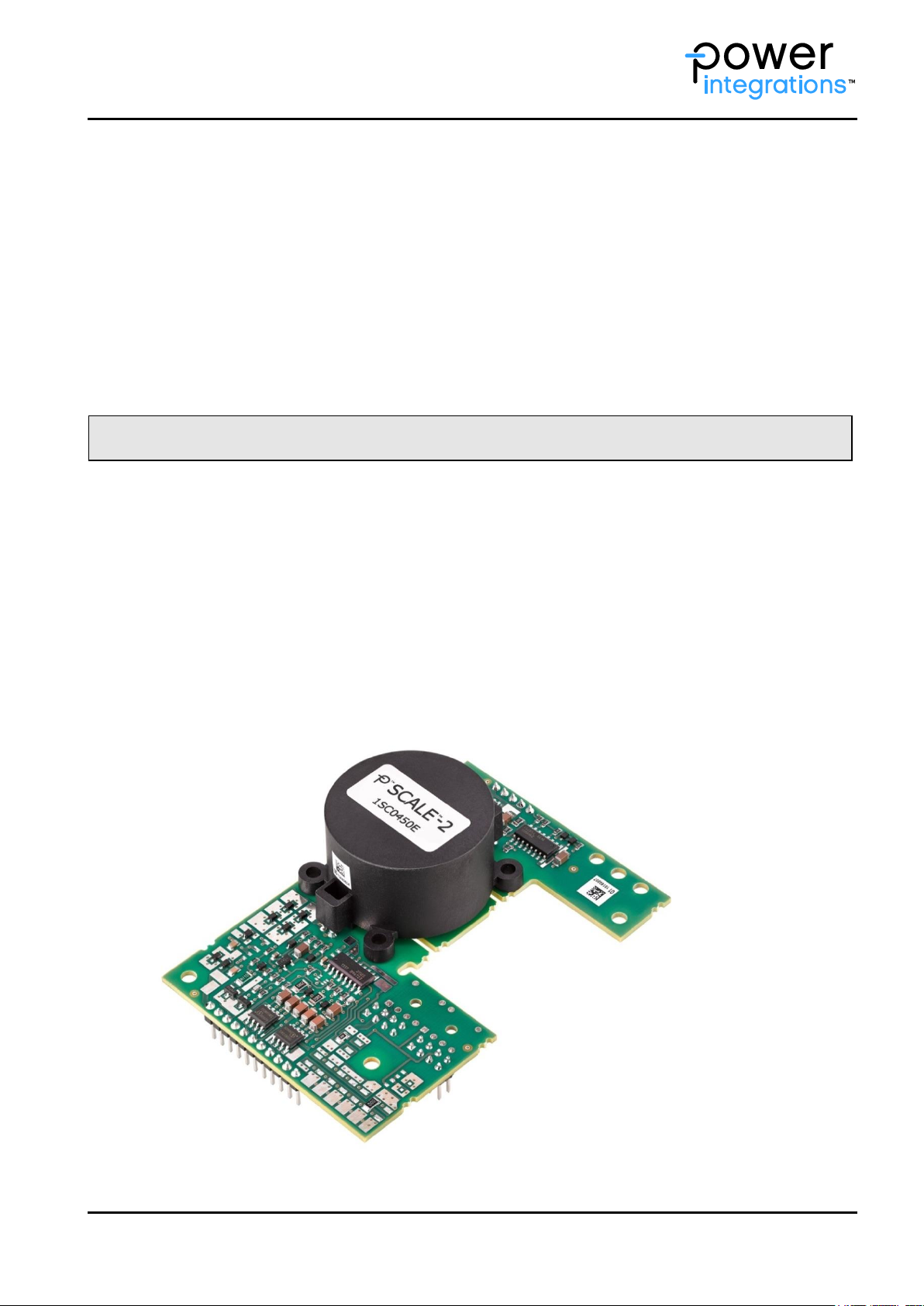
The 1SC0450E2B0 is the most compact driver core in its voltage and power range, featuring a footprint of
only 60mm x 90mm and a maximum insertion height of 27.5mm. It allows even the most restricted insertion
spaces to be efficiently used.
Fig. 1 1SC0450E2B0 driver core
www.power.com/igbt-driver Page 1
Page 2

SCALE™-2 1SC0450E2B0
Preliminary Description & Application Manual
Contents
Driver Overview ............................................................................................................................. 4
Mechanical Dimensions .................................................................................................................. 5
Pin Designation .............................................................................................................................. 7
Recommended Interface Circuitry for the Primary-Side Connector .............................................. 8
Description of Primary-Side Interface ........................................................................................... 8
General ............................................................................................................................... 8
VCC terminal ....................................................................................................................... 8
VDC terminal ....................................................................................................................... 8
GND ................................................................................................................................... 9
SO (status output) ............................................................................................................... 9
Recommended Interface Circuitry for the Secondary Side Connectors ........................................ 9
Pins 6 to 16 ......................................................................................................................... 9
Pins 17 to 32 ..................................................................................................................... 10
Description of Secondary-Side Interfaces ................................................................................... 10
General ............................................................................................................................. 10
DC/DC output (VISO), emitter (VE) and COM terminals ......................................................... 11
Reference terminal (REF) ................................................................................................... 11
Collector sense (VCE) ......................................................................................................... 11
Input for adjusting the turn-off delay in fault condition (CSHD) ............................................. 14
Active Clamping (ACL) ........................................................................................................ 15
Gate turn-on (GH) and turn-off (GL) terminals ..................................................................... 15
Gate Boosting Power Supply (VGB) ..................................................................................... 16
Gate Boosting Signal (GBS) ................................................................................................ 16
Gate Drive Input (IN) ......................................................................................................... 16
Status Feedback /Fault input (OUT) .................................................................................... 16
How Do 1SC0450E2B0 SCALE-2 Drivers Work in Detail? ............................................................ 19
Power supply and electrical isolation ................................................................................... 19
Power-supply monitoring .................................................................................................... 19
Parallel connection of IGBT modules ................................................................................... 19
3-level or multilevel topologies ............................................................................................ 19
Gate Boosting .................................................................................................................... 20
Bibliography ................................................................................................................................. 22
The Information Source: SCALE-2 Driver Data Sheets ................................................................ 23
Quite Special: Customized SCALE-2 Drivers ................................................................................ 23
Technical Support ........................................................................................................................ 23
Quality .......................................................................................................................................... 23
Legal Disclaimer ........................................................................................................................... 23
www.power.com/igbt-driver Page 2
Page 3

SCALE™-2 1SC0450E2B0
Preliminary Description & Application Manual
Ordering Information ................................................................................................................... 24
Information about Other Products .............................................................................................. 24
Power Integrations Sales Offices ................................................................................................. 25
www.power.com/igbt-driver Page 3
Page 4
SCALE™-2 1SC0450E2B0
Preliminary Description & Application Manual
Driver Overview
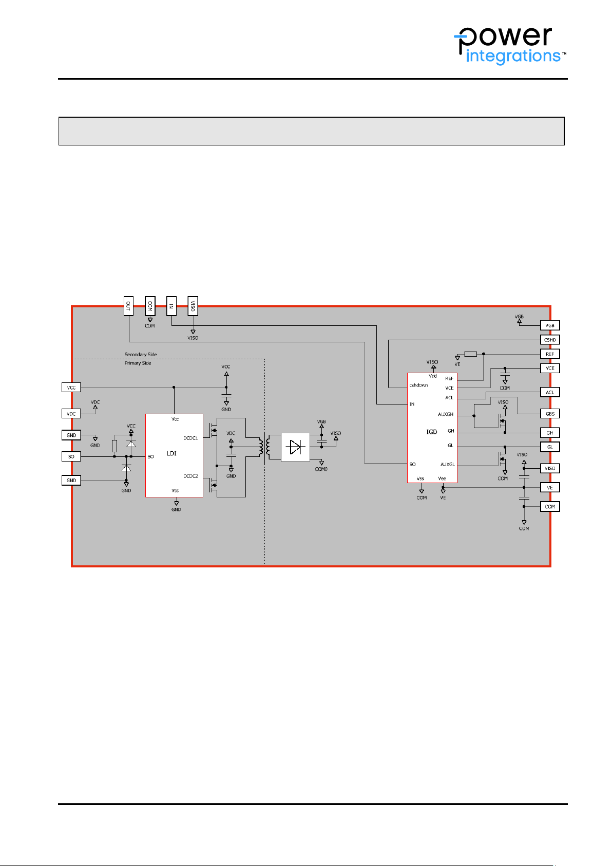
The 1SC0450E2B0 is a driver core equipped with the latest SCALE-2 chipset from Power Integrations /1/.
The SCALE-2 chipset comprises a set of application-specific integrated circuits (ASICs) that cover the main
functions needed to design intelligent gate drivers. The SCALE-2 driver chipset is a further development of
the proven SCALE™-1 technology /2/.
The 1SC0450E2B0 targets medium- and high-power IGBT applications up to 6500V. The driver supports
switching frequencies up to 10kHz with best-in-class efficiency. The 1SC0450E2B0 comprises a complete
single-channel IGBT driver core, fully equipped with an isolated DC/DC converter, electrical interface for the
external use of fiber-optic transceivers, short-circuit protection, Advanced Active Clamping and supplyvoltage monitoring. Additional features such as gate boosting are also implemented and provide further
driving benefits.
Fig. 2 Block diagram of the 1SC0450E2B0 driver core
www.power.com/igbt-driver Page 4
Page 5

SCALE™-2 1SC0450E2B0
Preliminary Description & Application Manual
Mechanical Dimensions
Fig. 3 Interactive 3D drawing of the 1SC0450E2B0
www.power.com/igbt-driver Page 5
Page 6
SCALE™-2 1SC0450E2B0
Preliminary Description & Application Manual
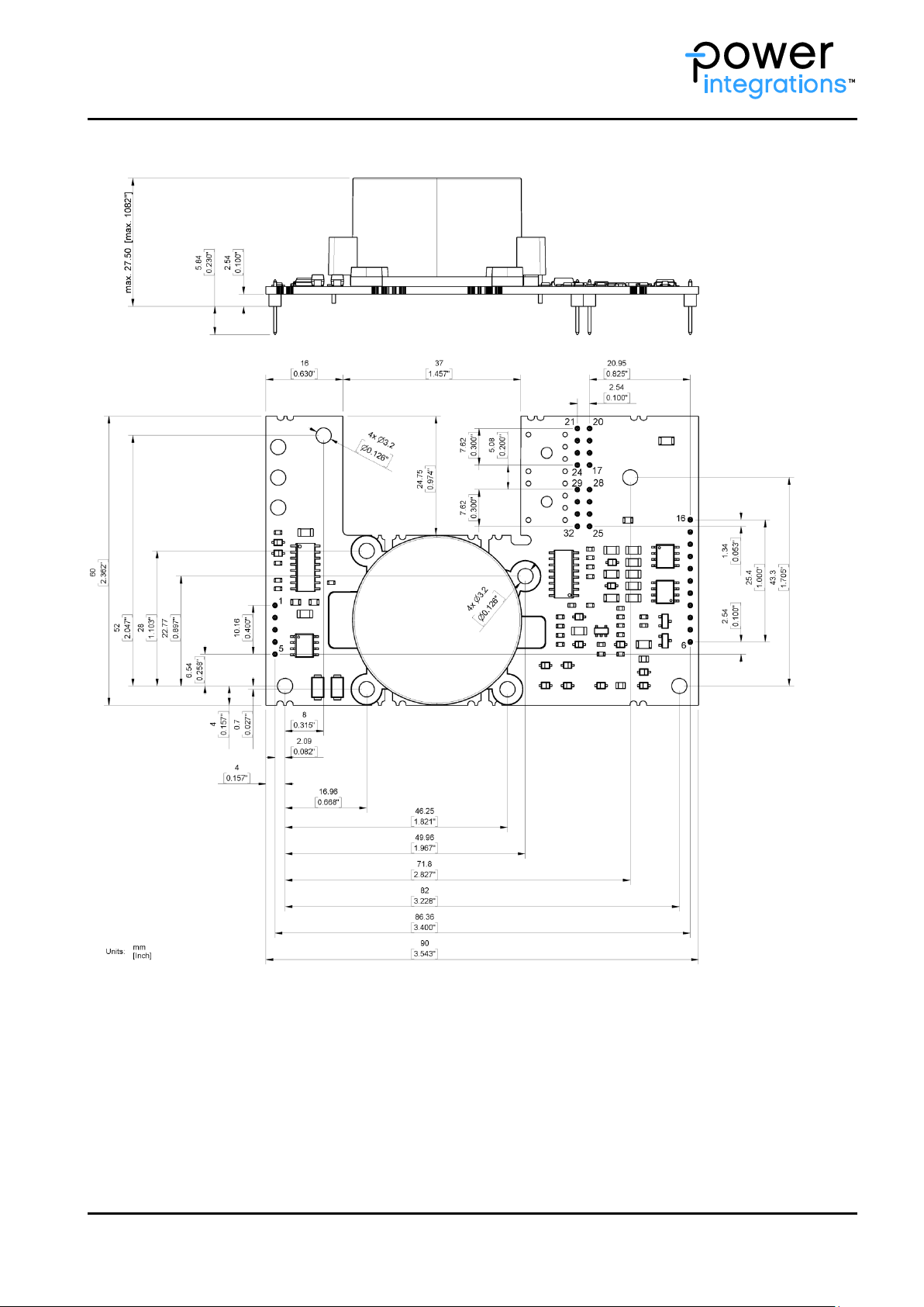
Fig. 4 Mechanical drawing of the 1SC0450E2B0
The primary-side and secondary-side pin grid is 2.54mm (100mil) with a pin cross-section of
0.64mm x 0.64mm. Total outline dimensions of the board are 60mm x 90mm. The total height of the driver
is maximum 27.5mm measured from the bottom of the pin bodies to the top of the populated PCB.
Note that the mechanical fixing points are placed in the clearance and creepage paths. Insulated fixation
material (screws, distance bolts) must therefore be used in order not to reduce these. The fixing points
support M3 screw size.
Recommended diameter of solder pads: Ø 2mm (79mil)
Recommended diameter of drill holes: Ø 1mm (39mil)
www.power.com/igbt-driver Page 6
Page 7

SCALE™-2 1SC0450E2B0
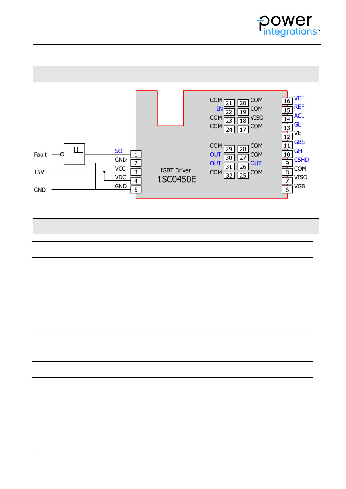
Pin No. and Name
Function
Primary Side
1 SO
Status output primary side; normally pulled up to VCC over a 10kΩ resistor, pulled
down to low in case of a fault
2 GND
Ground
3 VCC
Supply voltage; 15V supply for primary side
4 VDC
DC/DC converter supply
5 GND
Ground
Secondary Side
6 VGB
Gate-boosting power supply
7 VISO
DC/DC output
8 COM
Secondary-side ground
9 CSHD
Set turn-off delay after fault detection; capacitor to COM
10 GH
Gate high; pulls gate high through turn-on resistor
11 GBS
Gate-boosting signal
12 VE
IGBT emitter
13 GL
Gate low; pulls gate low through turn-off resistor
14 ACL
Active clamping feedback; leave open if not used
15 REF
Set VCE detection threshold through resistor to VE
16 VCE
VCE sense; connect to IGBT collector through impedance network
17 COM
Secondary-side ground
18 VISO
DC/DC output
19 COM
Secondary-side ground
20 COM
Secondary-side ground
21 COM
Secondary-side ground
22 IN
Gate driving input; Inverted non-isolated signal input
23 COM
Secondary-side ground
24 COM
Secondary-side ground
25 COM
Secondary-side ground
26 OUT
Status output and external fault input
27 COM
Secondary-side ground
28 COM
Secondary-side ground
29 COM
Secondary-side ground
30 OUT
Status output and external fault input
31 OUT
Status output and external fault input
32 COM
Secondary-side ground
Preliminary Description & Application Manual
Pin Designation
www.power.com/igbt-driver Page 7
Page 8
SCALE™-2 1SC0450E2B0
Preliminary Description & Application Manual
Recommended Interface Circuitry for the Primary-Side Connector
Fig. 5 Recommended user interface of the 1SC0450E2B0 (primary side)
Description of Primary-Side Interface
General
The primary-side interface of the 1SC0450E2B0 driver is very simple and easy to use.
The driver primary side is equipped with a 5-pin interface connector with the following terminals:
2x power-supply terminals VCC and VDC
2x ground terminals GND
1x status output SO (indicating a fault during primary-side under-voltage)
All inputs and outputs are ESD-protected.
VCC terminal
The driver has one VCC terminal on the interface connector to supply the primary-side electronics with 15V.
VDC terminal
The driver has one VDC terminal on the interface connector to supply the DC/DC converter for the secondary
side.
VDC should be supplied with 15V. It is recommended to connect the VCC and VDC terminals to a common
15V power supply. In that case, the driver limits the inrush current at startup and no external current
limitation of the voltage source for VDC is needed.
www.power.com/igbt-driver Page 8
Page 9

SCALE™-2 1SC0450E2B0
Preliminary Description & Application Manual
GND
Both ground pins must be connected together with low parasitic inductance. A common ground plane is
strongly recommended. Furthermore it is recommended to shield all primary-side circuitry with the ground
plane. The connecting distance between the ground pins must be kept to a minimum.
SO (status output)
When no primary-side under-voltage condition is detected, an internal pull-up resistor of 10kΩ keeps the
output level at the voltage level of VCC. When a primary-side supply under-voltage is detected, the status
output SO goes to low (connected to GND). The SO output is automatically reset (returning to the voltage
level of VCC) when the under-voltage on the primary side disappears.
The maximum SO current in a fault condition must not exceed the value specified in the driver data sheet
/3/.
Recommended Interface Circuitry for the Secondary Side Connectors
Pins 6 to 16
Fig. 6 Recommended user interface of the 1SC0450E2B0 (secondary-side pins 6 to 16) without gate
boosting (refer to chapter “Gate Boosting” and Fig. 11 for gate-boosting circuitry)
www.power.com/igbt-driver Page 9
Page 10

SCALE™-2 1SC0450E2B0
Preliminary Description & Application Manual
Pins 17 to 32
Fig. 7 Recommended command interface circuitry with Avago fiber-optic links HFBR-x522ETZ
Description of Secondary-Side Interfaces
General
The driver’s secondary side is equipped with an 11-pin and two 8-pin interface connectors.
The 11-pin interface connector features the following terminals:
1x DC/DC output terminal VISO
1x emitter terminal VE
1x secondary-side ground COM
1x collector sense terminal VCE
1x reference terminal REF for short-circuit protection
1x input terminal CSHD to set the turn-off delay after fault
1x active clamping terminal ACL
1x turn-on gate terminal GH
1x turn-off gate terminal GL
1x gate-boosting power supply VGB
1x gate-boosting signal GBS
The two 8-pin interface connectors combine the command interface and feature the following terminals:
1x DC/DC output terminal VISO
11x secondary-side ground COM
1x PWM input (inverted)
3x status feedback input/output (inverted)
All inputs and outputs are ESD-protected.
www.power.com/igbt-driver Page 10
Page 11

SCALE™-2 1SC0450E2B0
C1[μF]≥(QG[μC]-4.7)∙4
C1 in Fig. 6; 4µF blocking capacitance
per 1µC gate charge between VISO
and VE
Eq. 1
C2=
C
1
2
C2 in in Fig. 6; blocking capacitance
between VE and COM, half of the C1
value
Eq. 2
R
th
kΩ
=
68∙Vth[V]
10.2-Vth[V]
with Vth<10.2V
Eq. 3
R
tot
= R
vcei
=
n
i=1
R
vce1
+...+R
vcen
Eq. 4
Preliminary Description & Application Manual
DC/DC output (VISO), emitter (VE) and COM terminals
The driver is equipped with blocking capacitors on the secondary side of the DC/DC converter (for values
refer to the data sheet /3/). IGBTs with a gate charge of up to 4.7µC can be driven without additional
external capacitors (C1 and C2 in Fig. 6 are not assembled). Eq. 1 and Eq. 2 give the recommended
capacitance value of C1 and C2 for gate charges above this value:
Example: IGBT modules with a gate charge of up to 42µC can be driven with external capacitances of
149.2µF between the VISO and VE terminals and 74.6µF between the VE and COM terminals (C1
and C2 of Fig. 6).
If the capacitance C1 (or C2) exceeds 200µF (or 100µF), please contact the Power Integrations support
service.
The blocking capacitors must be connected as close as possible to the driver’s terminal pins with minimum
inductance. Ceramic capacitors with a dielectric strength ≥25V are recommended.
No static load must be applied between VISO and VE, or between VE and COM. A static load can be applied
between VISO and COM if necessary.
Reference terminal (REF)
The reference terminal REF allows the threshold to be set for short-circuit protection with a resistor placed
between REF and VE (Rth of Fig. 6). An internal resistor of 68kΩ sets the default threshold value to 10.2V. It
can be reduced with the use of an external resistor Rth according to the following Eq. 3:
It is recommended to keep the reference voltage at its maximum default value of 10.2V (without using an
external resistor Rth).
Collector sense (VCE)
The collector sense must be connected to the IGBT collector with the circuit shown in Fig. 6 in order to
detect a short circuit condition.
General information and recommendations:
The overall value R
It is recommended to dimension the overall value R
about 0.6…0.8mA to flow through them at the maximum DC-link voltage (Eq. 5). This current must
not exceed 0.8mA. It is recommended to use series-connected resistors; the minimum creepage and
clearance distances required for the application must be considered and the maximum voltage,
www.power.com/igbt-driver Page 11
of the resistors R
tot
is calculated with equation Eq. 4:
vcei
of the resistors in order for a current I
tot
Vce
of
Page 12

SCALE™-2 1SC0450E2B0
I
Vce
V
DC-linkmax
R
tot
=0.6.0.8mA
Eq. 5
R
div
[kΩ]=R
tot
[kΩ]∙
V
th
V
+VGL[V]
V
CEth
V
-Vth[V]
(V
CEth
> Vth)
Eq. 6
C
tot
=
1
1
C
vcek
p
k=1
=1…4pF
Eq. 7
C
vce1
C
tot
=0.7…0.9∙
R
tot
R
vce1+Rvce2
Eq. 8
Preliminary Description & Application Manual
power and temperature rating of the resistors used must not be exceeded. Dimensioning
recommendations are given below.
All resistors R
R
allows the static threshold detection level V
div
divider with R
V
.
CEth
|VGL| is the absolute value of the gate-emitter turn-off voltage at the driver output. It depends on
the driver load and can be found in the driver data sheet /3/. Vth is the reference value set at the
reference terminal REF as described in the “Reference terminal (REF)” section.
(i ≥ 1) must have the same value.
vcei
). R
tot
can be calculated with Eq. 6 in order to determine the static detection level
div
to be increased if required (resistive voltage
CEth
The recommended range for the overall capacitance value C
All capacitances C
The capacitance C
with k≥2 must have the same value.
vcek
must be chosen such that the Eq. 8 is satisfied:
vce1
is given in Eq. 7:
tot
The maximum voltage rating of the resistors and capacitors used must not be exceeded. Peak
values and average values must be considered. Dimensioning recommendations are given below.
The diodes D
and D10 must have a very low leakage current and a blocking voltage of >40V (e.g.
9
BAS416). Schottky diodes must be explicitly avoided.
R
and Ca are used to set the response time.
a
Recommended values for 6500V IGBTs with DC-link voltages up to 4500V
R
vce1=Rvce2
R
C
C
C
R
R
=620kΩ (0603, 1%)
div
vce1
vce2=Cvce3
=22pF (C0G, 50V, 5%)
a
=not assembled
th
=refer to Table 1 below (0603, 1%)
a
This setup uses 30 resistors R
=…=R
=200kΩ (500mW, 400V
vce30
=15pF (C0G, 1000V, 5%)
=…=C
=22pF (C0G, 630V, 5%)
vce15
and 15 capacitors C
vcei
peak
, 1%)
and leads to a static desaturation detection
vcek
threshold of about 201V.
www.power.com/igbt-driver Page 12
Page 13

SCALE™-2 1SC0450E2B0
V
DC-Link
Ra=68kΩ
Ra=91kΩ
Ra=120kΩ
4500V
5.3µs
6.9µs
9.0µs
3000V
5.3µs
7.0µs
9.1µs
2250V
5.5µs
7.0µs
9.1µs
1500V
7.2µs
8.0µs
9.4µs
1125V
9.9µs
10.3µs
11.1µs
900V
14.1µs
14.1µs
14.2µs
V
DC-Link
Ra=68kΩ
Ra=91kΩ
Ra=120kΩ
3200V
5.1µs
6.8µs
8.8µs
2000V
5.2µs
6.8µs
8.9µs
1500V
6.1µs
7.0µs
8.9µs
1000V
8.8µs
9.3µs
10.3µs
800V
12.7µs
13.1µs
12.9µs
Preliminary Description & Application Manual
Table 1 Typical response time as a function of the resistance Ra and the DC-link voltage V
DC-Link
Table 1 gives indicative values only. The response time depends on the specific layout and the IGBT module
used. It is therefore recommended to measure the short-circuit duration in the final design.
Note that slow IGBT modules may report a wrong VCE desaturation fault at turn-on. It is therefore
recommended to test the setup under worst case conditions (maximum DC-link voltage, maximum collector
current and highest IGBT junction temperature). Please also refer to AN-1101 /4/ for more information.
Recommended values for 4500V IGBTs with DC-link voltages up to 3200V
R
vce1=Rvce2
R
C
C
C
R
R
=620kΩ (0603, 1%)
div
vce1
vce2=Cvce3
=22pF (C0G, 50V, 5%)
a
=not assembled
th
=refer to Table 2 below (0603, 1%)
a
This setup uses 20 resistors R
=…=R
=220kΩ (500mW, 400V
vce20
=15pF (C0G, 1000V, 5%)
=…=C
=22pF (C0G, 630V, 5%)
vce10
and 10 capacitors C
vcei
peak
, 1%)
and leads to a static desaturation detection
vcek
threshold of about 150V.
Table 2 Typical response time as a function of the resistance Ra and the DC-link voltage V
DC-Link
Table 2 gives indicative values only. The response time depends on the specific layout and the IGBT module
used. It is therefore recommended to measure the short-circuit duration in the final design.
Note that slow IGBT modules may report a wrong VCE desaturation fault at turn-on. It is therefore
recommended to test the setup under worst case conditions (maximum DC-link voltage, maximum collector
current and highest IGBT junction temperature). Please also refer to AN-1101 /4/ for more information.
www.power.com/igbt-driver Page 13
Page 14

SCALE™-2 1SC0450E2B0
V
DC-Link
Ra=68kΩ
Ra=91kΩ
Ra=120kΩ
2200V
5.3µs
7.0µs
9.0µs
1500V
5.3µs
7.0µs
9.0µs
1100V
5.4µs
7.0µs
9.1µs
700V
7.6µs
8.1µs
9.3µs
600V
17.0µs
14.4µs
13.7µs
Circuit at pin CSHD
Typical turn-off delay T
cshd
Left open:
T
cshd
=0.2μs
Eq. 9
Capacitor between CSHD and COM:
T
cshd
[μs]=
C
cshd
[pF]
50
(C
cshd
≤10nF)
Eq. 10
Preliminary Description & Application Manual
Recommended values for 3300V IGBTs with DC-link voltages up to 2200V
R
vce1=Rvce2
R
C
C
C
R
R
=1.5MΩ (0603, 1%)
div
vce1
vce2=Cvce3
=22pF (C0G, 50V, 5%)
a
=not assembled
th
=refer to Table 3 below (0603, 1%)
a
This setup uses 14 resistors R
=…=R
=220kΩ (500mW, 400V
vce14
=15pF (C0G, 1000V, 5%)
=…=C
=22pF (C0G, 630V, 5%)
vce7
and 7 capacitors C
vcei
, 1%)
peak
per channel and leads to a static desaturation
vcek
detection threshold of about 50V.
Table 3 Typical response time as a function of the resistance Ra and the DC-link voltage V
DC-Link
Table 3 gives indicative values only. The response time depends on the specific layout and the IGBT module
used. It is therefore recommended to measure the short-circuit duration in the final design.
Note that slow IGBT modules may report a wrong VCE desaturation fault at turn-on. It is therefore
recommended to test the setup under worst case conditions (maximum DC-link voltage, maximum collector
current and highest IGBT junction temperature). Please also refer to AN-1101 /4/ for more information.
Input for adjusting the turn-off delay in fault condition (CSHD)
The terminal CSHD allows the delay in turning off the IGBT after a fault detection on the driver’s secondary
side (short-circuit, undervoltage, external fault input) to be determined with a capacitor C
a maximum value of 10nF connected to COM. Table 4 shows the resulting delay as a function of the circuit
used at pin CSHD.
Table 4 Turn-off delay as a function of CSHD wiring
As soon as the fault turn-off delay time T
has elapsed, the driver’s channel is automatically turned off.
cshd
The driver’s channel can also be turned off from the driver’s input IN within the turn-off delay time T
determined by the CSHD pin after a secondary-side fault detection.
(C0G/50V) with
cshd
cshd
Note that it will not be possible to turn the IGBT on during about 100ns per 100pF capacitance applied to
CSHD after a fault condition, starting from the turn-off event of the IGBT (minimum off-time required).
www.power.com/igbt-driver Page 14
Page 15

SCALE™-2 1SC0450E2B0
Preliminary Description & Application Manual
Active Clamping (ACL)
Active clamping is a technique designed to partially turn on the power semiconductor as soon as the
collector-emitter voltage exceeds a predefined threshold. The power semiconductor is then kept in linear
operation.
Basic active clamping topologies implement a single feedback path from the IGBT’s collector through
transient voltage suppressor devices (TVS) to the IGBT gate. The 1SC0450E2B0 supports Advanced Active
Clamping from Power Integrations, where the feedback is also provided to the driver’s secondary side at pin
ACL (Fig. 6): as soon as the voltage at pin ACL exceeds about 1.3V, the turn-off MOSFET is progressively
switched off in order to improve the effectiveness of the active clamping and to reduce the losses in the
TVS. The turn-off MOSFET is turned completely off when the voltage at pin ACL approaches 20V (measured
to COM).
It is recommended to use the circuit shown in Fig. 6. The following parameters must be adapted to the
application:
For TVS D
At least one bidirectional TVS (D1) (≥300V for 3300V IGBTs, ≥350V for 4500V IGBTs, ≥440V for
6500V IGBTs) must be used in order to avoid negative current flowing through the TVS chain during
turn-on of the anti-parallel diode of the IGBT module due to its forward recovery behavior. Such a
current could, depending on the application, lead to under-voltage of the driver secondary-side
voltage VISO to VE (15V).
Note that it is possible to modify the number of TVS in a chain. The active clamping efficiency can
be improved by increasing the number of TVS used in a chain if the total breakdown voltage remains
at the same value. Note also that the active clamping efficiency is highly dependent on the type of
TVS used (e.g. manufacturer).
D
and D4: It is recommended to use Schottky diodes with blocking voltages >35V (>1A depending on
3
the application).
, D2 it is recommended to use:
1
- 3300V IGBTs with DC-link voltages up to 2200V: Seven unidirectional 300V TVS and one
bidirectional 350V TVS. Good clamping results can be obtained with seven unidirectional TVS
P6SMB300A and one bidirectional TVS P6SMB350CA from Diotec.
- 4500V IGBTs with DC-link voltages up to 3200V: Eight unidirectional 400V TVS and one
bidirectional 350V TVS. Good clamping results can be obtained with eight unidirectional TVS
P6SMB400A and one bidirectional TVS P6SMB350CA from Diotec.
- 6500V IGBTs with DC-link voltages up to 4350V: Ten unidirectional 440V TVS and one
bidirectional 440V TVS. Good clamping results can be obtained with ten unidirectional TVS
P6SMB440A and one bidirectional TVS P6SMB440CA from Diotec.
Please note that the diodes D3 and D4 must not be omitted if Advanced Active Clamping is used.
If active clamping is not used, the diode D4 can be omitted. The pin ACLx must then be left open.
Gate turn-on (GH) and turn-off (GL) terminals
These terminals allow the turn-on (GH) and turn-off (GL) gate resistors to be connected to the gate of the
power semiconductor. The GH and GL pins are available as separated terminals in order to set the turn-on
and turn-off resistors independently without the use of an additional diode. Please refer to the driver data
sheet /3/ for the limit values of the gate resistors used.
A resistor between GL and COM of 6.8kΩ (other values are also possible) may be used in order to provide a
low-impedance path from the IGBT gate to the emitter even if the driver is not supplied with power. No
static load (e.g. resistors) must be placed between GL and the emitter terminal VE.
www.power.com/igbt-driver Page 15
Page 16

SCALE™-2 1SC0450E2B0
Drive Signal
T/R
(1)
Light
Input IN
Gate Output
Low
Off
High
Off-state
High
On
Low
On-state
Preliminary Description & Application Manual
Note, however, that it is not advisable to operate the power semiconductors within a half-bridge with a
driver in the event of a low supply voltage. Otherwise, a steep increase of VCE may cause partial turn-on of
these IGBTs.
Gate Boosting Power Supply (VGB)
The driver supports an increased IGBT turn-on voltage source VGB to perform gate boosting. The voltage is
generated by internal circuitry. No static load must be applied to VGB. Refer to the driver data sheet /3/ for
more information.
Gate Boosting Signal (GBS)
The gate-boosting signal GBS is an auxiliary signal that has the same time waveform – but different voltage
values – as the GH signal. Please refer to the driver data sheet for the exact voltage values /3/ and to the
”Gate Boosting” section for more information.
Note that no static load must be applied to GBS. Refer to the driver data sheet /3/ for more information.
Gate Drive Input (IN)
The gate drive input signal IN is inverted to the gate output. A transition to a low-level state at IN generates
a driver turn-on command while a transition to a high-level state generates a driver turn-off command. Also
refer to Table 5 and Fig. 8.
It is recommended to use the input circuitry of Fig. 7. The drive signal is then not inverted to the gate
output according to Table 5.
If other drive circuits are used, the following information must be considered:
The absolute maximum ratings of the driver data sheet /3/ must be respected.
The logic level thresholds of the input IN are given in the driver data sheet /3/.
The input IN features an internal pull-up current source of about 500µA which sets its potential to a
high-level state and assures an IGBT off-state condition if the pin is floating. Refer to the driver data
sheet /3/ for values.
Pin IN belongs to the secondary-side electrical circuit and follows the emitter potential of the driven
IGBT. It must be isolated against primary-side circuits, e. g. with fiber-optic links.
Table 5 Signal input truth table correlated with the schematics of Fig. 7
Status Feedback /Fault input (OUT)
The OUT terminal is mainly used as a status feedback output. However, it also works as an input. When
OUT is externally shorted to COM for a minimum period of time (timing and threshold values according to
the driver data sheet /3/), the driver detects an external fault. The IGBT is then turned off after a delay
(1)
www.power.com/igbt-driver Page 16
T/R: Transmitter and receiver pair of a fiber-optic link
Page 17

SCALE™-2 1SC0450E2B0
Preliminary Description & Application Manual
T
(refer to the chapter “Input for adjusting the turn-off delay in fault condition (CSHD)”). Note that
CSHD
failure to respect the minimum hold time may lead to incorrect driver behavior.
The recommended circuitry for using the OUT terminal as an external fault input is shown in Fig. 7
(transistor connected to “External fault input”). The external effective capacitance (components and board
parasitic capacitances referred to VISO, VE and COM) must not exceed the value given in the driver data
sheet /3/ to avoid unexpected driver fault triggering in normal operation.
In normal operation, each edge of the control signal IN is acknowledged by the driver with a short pulse
(OUT is switched to low for a short period of time; refer to driver data sheet /3/ for details). As this can be
observed by the host controller, this method allows simple and continuous monitoring of all drivers and
fiber-optic links of the system (Fig. 8).
Fig. 8 Driver behavior and status feedback in normal operation (Refer to Fig. 7 for the recommended
command interface)
The driver can detect three different secondary-side faults:
V
Secondary-side supply under-voltage; refer to chapter “Power-supply monitoring”
External fault (as described above)
The signal truth table of Table 6 shows the behavior of the OUT signal in normal operation as well as in a
fault condition. Only the pulse length of OUT differs between normal operation (acknowledge) and the
different fault conditions.
www.power.com/igbt-driver Page 17
-desaturation detection in case of a short-circuit; refer to chapter “Collector sense (VCE)”
CE
Page 18

SCALE™-2 1SC0450E2B0
Status
OUT
T/R
(2)
Light
Status Feedback
Idle
High
On
Low
Acknowledge
or fault pulse
Low
Off
High
Preliminary Description & Application Manual
Table 6 Signal truth table correlated with the schematics of Fig. 7
Fig. 9 shows the response of the driver in the event of an IGBT short-circuit condition. The fault status is
transferred to the status feedback terminal after the response time. The light is then driven “off” during the
delay to clear the fault state (8μs+T
T
. The IGBT can be turned on again by applying a negative edge to the input IN after the fault status has
cshd
disappeared.
). The driver turns the IGBT off after the response time + delay time
cshd
Fig. 9 Driver behavior and status feedback in the IGBT short-circuit condition
In case of a secondary-side supply under-voltage fault, the fault status remains active as long as this undervoltage remains. The driver response in the event of a supply under-voltage on VISO-VE is shown in Fig. 10.
Fig. 10 Status feedback in the event of a secondary-side supply under-voltage
(2)
T/R: Transmitter and receiver pair of a fiber-optic link
www.power.com/igbt-driver Page 18
Page 19

SCALE™-2 1SC0450E2B0
Preliminary Description & Application Manual
During power-up, the status feedback will also show a fault condition until the supply under-voltage
protection disappears.
If the OUT terminal is not used, it is recommended to connect the OUT pin to VISO via a pull-up resistor in
the range of 1.5kΩ to 10kΩ.
How Do 1SC0450E2B0 SCALE-2 Drivers Work in Detail?
Power supply and electrical isolation
The driver is equipped with a DC/DC converter to provide an electrically insulated power supply to the gate
driver circuitry. The transformer features basic insulation according to IEC 61800-5-1 as well as IEC 60664-1
between the primary and secondary sides.
Note that the driver requires a stabilized supply voltage.
Power-supply monitoring
The driver’s primary and secondary sides are equipped with a local under-voltage monitoring circuit.
In the event of a primary-side supply under-voltage, the under-voltage is signalized by the electrical status
output SO. A primary-side under-voltage will not automatically cause a gate turn-off command. This
condition has to be detected by the control logic which has to switch off and block the gate drive signal.
In case of a secondary-side supply under-voltage, the corresponding power semiconductor is driven with a
negative gate voltage after the delay in IGBT turn-off (refer to “Input for adjusting the turn-off delay in fault
condition (CSHD)”) to keep it in the off-state (the channel is blocked) and a fault condition is monitored on
the status output OUT until the supply voltage exceeds the reference level for enabling.
Parallel connection of IGBT modules
It is recommended to drive parallel-connected IGBT modules using a single 1SC0450E2B0 driver core.
Appropriate gate circuitry has to be used. Please contact the Power Integrations support service for more
information.
3-level or multilevel topologies
In applications with multi-level topologies, the turn-off sequence of the individual power semiconductors
usually needs to be controlled by the host controller in case of a detected fault condition (e.g. short circuit,
over-current), especially if no Advanced Active Clamping or Dynamic Advanced Active Clamping is
implemented.
In that case, the turn-off delay in the fault condition of the different drivers can be adjusted to match the
corresponding timing specifications. It is in particular possible to determine a specific turn-off delay for the
inner IGBTs of a 3-level NPC topology as described in the section: “Input for adjusting the turn-off delay in
fault condition (CSHD)”. The driver’s response time can also be adapted accordingly if required.
Note however that Advanced Active Clamping offers simple and safe protection that allows excessive
collector-emitter overvoltages to be avoided in case of wrong commutation sequences in the short-circuit
condition of 3-level converter topologies (refer to /6/ and /7/ for more information).
www.power.com/igbt-driver Page 19
Page 20

SCALE™-2 1SC0450E2B0
C
gb
nF
=
Q
gb
nC
VGH[V]+VGL[V]
-22
Cgb≥0
Eq. 11
T
min
μs
=11∙ 1+
22+C
gb
nF
22
+T
gb
[μs]
Eq. 12
P
gb
W
=10
-6
∙C
gb
nF
+22+6.5∙T
gb
μs
∙
V
GH
V
V
GL
V
∙f[kHz]
Eq. 13
Preliminary Description & Application Manual
Gate Boosting
The 1SC0450E2B0 driver supports gate boosting. This feature allows the commutation speed of the
collector-emitter voltage to be accelerated at turn-on after the critical phase of the diode reverse recovery
behavior to reduce the IGBT turn-on losses.
A dedicated external circuit as shown in Fig. 11 is required. Detailed gate-boosting recommendations are not
currently available.
Gate-boosting circuit principle
The “Gate Boosting Logic” according to Fig. 11 has to trigger the boosting function at the appropriate time
during the IGBT turn on transition as illustrated in Fig. 12:
The delay time between GBS and the required boosting time needs to be determined by the “Gate
Boosting Logic” circuit.
The pulse length of the boosting pulse also needs to be determined by the “Gate Boosting Logic”
circuit. It must be limited to a few microseconds.
A turn-on pulse of the gate-boosting power switch Q1 will be generated. This will lead to an increased turnon gate current that will be injected into the IGBT gate over Rgb.
The boosting charge capability can be increased by adding an external capacitor Cgb. The minimum value Cgb
of the external capacitor can be calculated according to Eq. 11.
where Qgb stands for the required boosting gate charge and has to be determined according to the IGBT
module gate charge requirements. VGH and VGL are the absolute values of the turn-on and turn-off voltage at
the driver output respectively. Their value can be found in the driver data sheet /3/. Note that Eq. 11
assumes a full discharge of Cgb during a gate-boosting event (worst case).
The gate-boosting capability is further limited by the minimum time span between two consecutive gate
turn-on commands as well as by the gate-boosting power. The minimum required time T
between two
min
consecutive gate turn-on commands is given by Eq. 12. The gate-boosting efficiency is reduced if Eq. 12 is
not respected.
Tgb stands for the gate-boosting pulse length (Fig. 12). It is recommended to limit it to 1…5μs.
The maximum gate-boosting power must be within the absolute maximum ratings of the driver data sheet
/3/. Eq. 13 gives a worst case approximation of the real gate-boosting power Pgb. It is sufficient to design
the gate boosting such that Pgb is lower than the corresponding absolute maximum rating of the driver data
sheet /3/.
www.power.com/igbt-driver Page 20
Page 21

SCALE™-2 1SC0450E2B0
Preliminary Description & Application Manual
Fig. 11 Gate-boosting circuit principle – highlighted in red color
Fig. 12 Gate-boosting signals
How to disable gate boosting?
Pins VGB and GBS must be left open. Note that the voltage values of the pins VGB and GBS are 50V and 35V
respectively referred to COM (creepage and clearance distances).
www.power.com/igbt-driver Page 21
Page 22

SCALE™-2 1SC0450E2B0
Preliminary Description & Application Manual
Bibliography
/1/ Paper: Smart Power Chip Tuning, Bodo’s Power Systems, May 2007
/2/ “Description and Application Manual for SCALE™ Drivers”, Power Integrations
/3/ Data sheet SCALE™-2 driver core 1SC0450E2B0, Power Integrations
/4/ Application note AN-1101: Application with SCALE™-2 and SCALE™-2+ Gate Driver Cores, Power
Integrations
/5/ Application note AN-0904: Direct Paralleling of SCALE™-2 Gate Driver Cores, Power Integrations
/6/ Application note AN-0901: Methodology for Controlling Multi-Level Converter Topologies with
SCALE™-2 IGBT Drivers, Power Integrations
/7/ Paper: Safe Driving of Multi-Level Converters Using Sophisticated Gate Driver Technology, PCIM
Asia, June 2013
Note: The Application Notes are available on the Internet at www.power.com/igbt-driver/go/app-note and
the papers at www.power.com/igbt-driver/go/papers.
www.power.com/igbt-driver Page 22
Page 23

SCALE™-2 1SC0450E2B0
Preliminary Description & Application Manual
The Information Source: SCALE-2 Driver Data Sheets
Power Integrations offers the widest selection of gate drivers for power MOSFETs and IGBTs for almost any
application requirements. The largest website on gate-drive circuitry anywhere contains all data sheets,
application notes and manuals, technical information and support sections: www.power.com.
Quite Special: Customized SCALE-2 Drivers
If you need an IGBT driver that is not included in the delivery range, please don’t hesitate to contact Power
Integrations or your Power Integrations sales partners.
Power Integrations has more than 25 years of experience in the development and manufacturing of
intelligent gate drivers for power MOSFETs and IGBTs and has already implemented a huge number of
customized solutions.
Technical Support
Power Integrations provides expert help for your questions and problems:
www.power.com/igbt-driver/go/support
Quality
The obligation to high quality is one of the central features laid down in the mission statement of Power
Integrations Switzerland GmbH. Our total quality management system assures state-of-the-art processes
throughout all functions of the company, certified by ISO9001:2008 standards.
Legal Disclaimer
The statements, technical information and recommendations contained herein are believed to be accurate as
of the date hereof. All parameters, numbers, values and other technical data included in the technical
information were calculated and determined to our best knowledge in accordance with the relevant technical
norms (if any). They may base on assumptions or operational conditions that do not necessarily apply in
general. We exclude any representation or warranty, express or implied, in relation to the accuracy or
completeness of the statements, technical information and recommendations contained herein. No
responsibility is accepted for the accuracy or sufficiency of any of the statements, technical information,
recommendations or opinions communicated and any liability for any direct, indirect or consequential loss or
damage suffered by any person arising therefrom is expressly disclaimed.
www.power.com/igbt-driver Page 23
Page 24

SCALE™-2 1SC0450E2B0
Preliminary Description & Application Manual
Ordering Information
Our international terms and conditions of sale apply.
Type Designation Description
1SC0450E2B0-45 Single-channel SCALE-2 driver core for 4500V IGBTs
1SC0450E2B0-65 Single-channel SCALE-2 driver core for 6500V IGBTs
Product home page: www.power.com/igbt-driver/go/1SC0450
Refer to www.power.com/igbt-driver/go/nomenclature for information on driver nomenclature.
Information about Other Products
For other driver cores:
Direct link: www.power.com/igbt-driver/go/cores
For other drivers, product documentation and application support:
Please click: www.power.com
© 2014…2017 Power Integrations Switzerland GmbH. All rights reserved.
We reserve the right to make any technical modifications without prior notice. Version 1.0 from 2017-06-13
www.power.com/igbt-driver Page 24
Page 25

SCALE™-2 1SC0450E2B0
WORLD HEADQUARTERS
5245 Hellyer Avenue
San Jose, CA 95138 USA
Tel: +1-408-414-9200
Fax: +1-408-414-9765
Email: usasales@power.com
AMERICAS EAST
7360 McGinnis Ferry Road
Suite 225
Suwannee, GA 30024 USA
Tel: +1-678-957-0724
Fax: +1-678-957-0784
Email: usasales@power.com
AMERICAS CENTRAL
333 Sheridan Road
Winnetka, IL 60093 USA
Tel: +1-847-721-6293
Email: usasales@power.com
AMERICAS WEST
5245 Hellyer Avenue
San Jose, CA 95138 USA
Tel: +1-408-414-8778
Fax: +1-408-414-3760
Email: usasales@power.com
CHINA (Shanghai)
Room 2410, Charity Plaza
No. 88 North Caoxi Road
Shanghai, 200030 China
Tel: +86-21-6354-6323
Fax: +86-21-6354-6325
Email: chinasales@power.com
CHINA (Shenzhen)
17/F, Hivac Building, No 2
Keji South 8th Road, Nanshan District
Shenzhen, 518057 China
Tel: +86-755-8672-8689
Fax: +86-755-8672-8690
Email: chinasales@power.com
GERMANY (AC-DC/LED Sales)
Lindwurmstrasse 114
80337 München, Germany
Tel: +49-89-5527-39100
Fax: +49-89-1228-5374
Email: eurosales@power.com
GERMANY (IGBT Driver Sales)
HellwegForum 1
59469 Ense, Germany
Tel: +49-2938-64-39990
Email: igbt-driver.sales@power.com
INDIA (Bangalore)
#1, 14th Main Road
Vasanthangar
Bangalore, 560052 India
Tel 1: +91-80-4113-8020
Tel 2: +91-80-4113-8028
Fax: +91-80-4113-8023
Email: indiasales@power.com
INDIA (Mumbai)
Unit: 106-107, Sagar Tech Plaza-B
Sakinaka, Andheri Kurla Road
Mumbai, Maharashtra 400072 India
Tel 1: +91-22-4003-3700
Tel 2: +91-22-4003-3600
Email: indiasales@power.com
INDIA (New Dehli)
#45, Top Floor
Okhla Industrial Area, Phase - III
New Dehli, 110020 India
Tel 1: +91-11-4055-2351
Tel 2: +91-11-4055-2353
Email: indiasales@power.com
ITALY
Via Milanese 20
20099 Sesto San Giovanni (MI), Italy
Tel: +39-02-4550-8708
Email: eurosales@power.com
JAPAN
Kosei Dai-3 Bldg.
2-12-11, Shin-Yokohama, Kohoku-ku
Yokohama-shi, Kanagawa
Japan 222-0033
Tel: +81-45-471-1021
Fax: +81-45-471-3717
Email: japansales@power.com
KOREA
RM602, 6FL, 22
Teheran-ro 87-gil, Gangnam-gu
Seoul, 06164 Korea
Tel: +82-2-2016-6610
Fax: +82-2-2016-6630
Email: koreasales@power.com
SINGAPORE
51 Newton Road
#19-01/05 Goldhill Plaza
Singapore, 308900
Tel 1: +65-6358-2160
Tel 2: +65-6358-4480
Fax: +65-6358-2015
Email: singaporesales@power.com
TAIWAN
5F, No. 318, Nei Hu Rd., Sec. 1
Nei Hu Dist.
Taipei, 114 Taiwan
Tel: +886-2-2659-4570
Fax: +886-2-2659-4550
Email: taiwansales@power.com
UNITED KINGDOM
Bulding 5, Suite 21
The Westbrook Centre
Milton Road
Cambridge, CB4 1YG United Kingdom
Tel: +44-7823-557-484
Email: eurosales@power.com
Preliminary Description & Application Manual
Power Integrations Sales Offices
www.power.com/igbt-driver Page 25
 Loading...