


Title
Reference Design Report for a 35 W Power
Supply Using TOP258PN
90 VAC to 265 VAC Input
Specification
5 V, 2.2 A and 12 V, 2 A Output
Application
Author
LCD Monitor
Power Integrations Applications Department
Document
RDR-142
Number
Date
Revision
Summary and Features
• Low cost, low component count, high efficiency
• Delivers 35 W at 50°C ambient without requiring an external heat sink
• Meets output cross regulation requirements without linear regulators
• EcoSmart® – meets requirements for low no-load and standby power
consumption
• 0.42 W output power for <1 W input
• No-load power consumption < 300 mW at 230 VAC
• >82% full load efficiency
• Integrated safety/reliability features:
• Accurate, auto-recovering, hysteretic thermal shutdown function maintains
safe PCB temperatures under all conditions
• Auto-restart protects against output short circuits and open feedback loops
• Output OVP protection configurable for latching or self recovering
• Input UV prevents power up / power down output glitches
• Meets EN55022 and CISPR-22 Class B conducted EMI with > 10 dBµV margin
The products and applications illustrated herein (including circuits external to the products and transformer
construction) may be covered by one or more U.S. and foreign patents or potentially by pending U.S. and foreign
patent applications assigned to Power Integrations. A complete list of Power Integrations’ patents may be found at
www.powerint.com.
September 24, 2007
1.0
Power Integrations
5245 Hellyer Avenue, San Jose, CA 95138 USA.
Tel: +1 408 414 9200 Fax: +1 408 414 9201
www.powerint.com

RDR-142 35 W, TOP258PN Dual Output Supply 24-Sep-07
Table of Contents
1 Introduction................................................................................................................. 4
2 Power Supply Specification ........................................................................................ 5
3 Schematic...................................................................................................................6
4 Circuit Description ......................................................................................................7
4.1 Input EMI Filtering ...............................................................................................7
4.2 TOPSwitch-HX Primary.......................................................................................7
4.3 Output Rectification .............................................................................................8
4.4 Output Feedback.................................................................................................9
4.5 PCB Layout ....................................................................................................... 10
5 Bill of Materials ......................................................................................................... 11
6 Transformer Specification......................................................................................... 13
6.1 Electrical Diagram .............................................................................................13
6.2 Electrical Specifications..................................................................................... 13
6.3 Materials............................................................................................................13
6.4 Transformer Build Diagram ...............................................................................14
6.5 Transformer Construction.................................................................................. 15
7 Design Spreadsheet .................................................................................................16
8 Performance Data ....................................................................................................20
8.1 Efficiency ...........................................................................................................20
8.1.1 Active Mode CEC Measurement Data........................................................20
8.2 No-load Input Power.......................................................................................... 22
8.3 Available Standby Output Power.......................................................................23
9 Regulation ................................................................................................................24
9.1.1 Load ...........................................................................................................24
9.1.2 Line ............................................................................................................25
9.1.3 Cross Regulation Matrix .............................................................................26
10 Thermal Performance ...........................................................................................27
11 Waveforms............................................................................................................ 28
11.1 Drain Voltage and Current, Normal Operation...................................................28
11.2 Output Voltage Start-up Profile..........................................................................28
11.3 Drain Voltage and Current Start-up Profile ........................................................ 30
11.4 Load Transient Response (75% to 100% Load Step) .......................................31
11.5 Output Over-voltage Protection ......................................................................... 32
11.6 Output Ripple Measurements ............................................................................33
11.6.1 Ripple Measurement Technique ................................................................33
11.6.2 Measurement Results ................................................................................34
12 Line Surge.............................................................................................................35
13 Control Loop Measurements.................................................................................36
13.1 90 VAC Maximum Load..................................................................................... 36
13.2 265 VAC Maximum Load................................................................................... 36
14 Conducted EMI .....................................................................................................37
15 Revision History ....................................................................................................38
Important Note:
Page 2 of 40
Power Integrations, Inc.
Tel: +1 408 414 9200 Fax: +1 408 414 9201
www.powerint.com

24-Sep-07 RDR-142 35 W, TOP258PN Dual Output Supply
Although this board is designed to satisfy safety isolation requirements, the engineering
prototype has not been agency approved. Therefore, all testing should be performed
using an isolation transformer to provide the AC input to the prototype board.
Page 3 of 40
Tel: +1 408 414 9200 Fax: +1 408 414 9201
Power Integrations
www.powerint.com
RDR-142 35 W, TOP258PN Dual Output Supply 24-Sep-07
1 Introduction
This document is an engineering report describing a LCD Monitor power supply utilizing a
TOP258PN. This power supply is intended as a general purpose evaluation platform for
TOPSwitch-HX.
The document contains the power supply specification, schematic, bill of materials,
transformer documentation, printed circuit layout, and performance data.
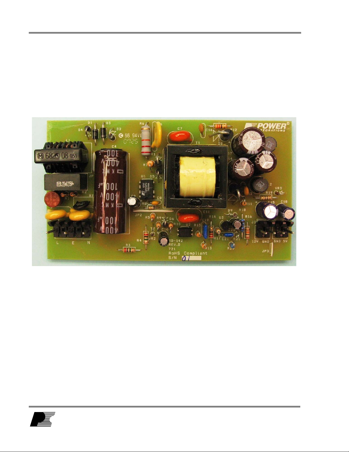
Figure 1 – Populated Circuit Board Photograph (5”L x 2.84”W x 1.16”H)
Page 4 of 40
Power Integrations, Inc.
Tel: +1 408 414 9200 Fax: +1 408 414 9201
www.powerint.com
24-Sep-07 RDR-142 35 W, TOP258PN Dual Output Supply
2 Power Supply Specification
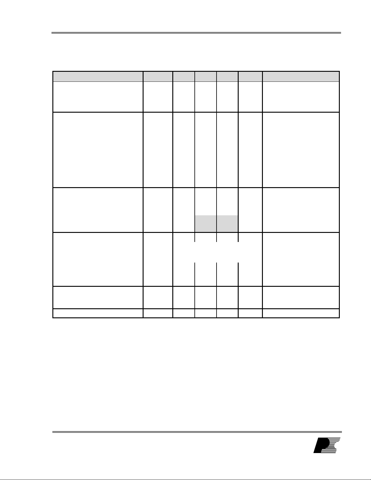
Description Symbol Min Typ Max Units Comment
Input
Voltage
Frequency
No-load Input Power (230 VAC) 0.3 W
Output
Output Voltage 1
Output Ripple Voltage 1
Output Current 1
Output Voltage 2
Output Ripple Voltage 2
Output Current 2
Total Output Power
Continuous Output Power
Efficiency
Full Load
Standby Input Power 1 W
Required average efficiency at
25, 50, 75 and 100 % of P
OUT
Environmental
Conducted EMI
Safety
Surge
Differential
Common Mode
Surge
Ring Wave
Ambient Temperature
*Shown for information only as CEC requirement does not apply to internal power supplies
V
f
LINE
IN
90 265 VAC
47 50/60 64 Hz
3 wire input
V
OUT1
V
RIPPLE1
I
OUT1
V
OUT2
V
RIPPLE2
I
OUT2
4.75 5 5.25 V
100 mV
0 2.2 A
9.6 12 14.4 V
500 mV
0 2 A
± 5%
20 MHz bandwidth
± 20%
20 MHz bandwidth
P
OUT
35 W
Measured at P
5 V @ 82 mA, 12 V @ 0 mA;
Vin at 264 VAC
Per California Energy Commission
(CEC) / Energy Star requirements
η
η
CEC
82 %
*
81
%
Meets CISPR22B / EN55022B
Designed to meet IEC950, UL1950
1
2
1 kV
0 50
T
AMB
Class II
1.2/50 µs surge, IEC 1000-4-5,
kV
kV
o
C
Series Impedance:
Differential Mode: 2 Ω
Common Mode: 12 Ω
100 kHz ring wave, 500 A short
circuit current, differential and
common mode
Free convection, sea level
OUT
25
o
C
Page 5 of 40
Tel: +1 408 414 9200 Fax: +1 408 414 9201
Power Integrations
www.powerint.com
RDR-142 35 W, TOP258PN Dual Output Supply 24-Sep-07
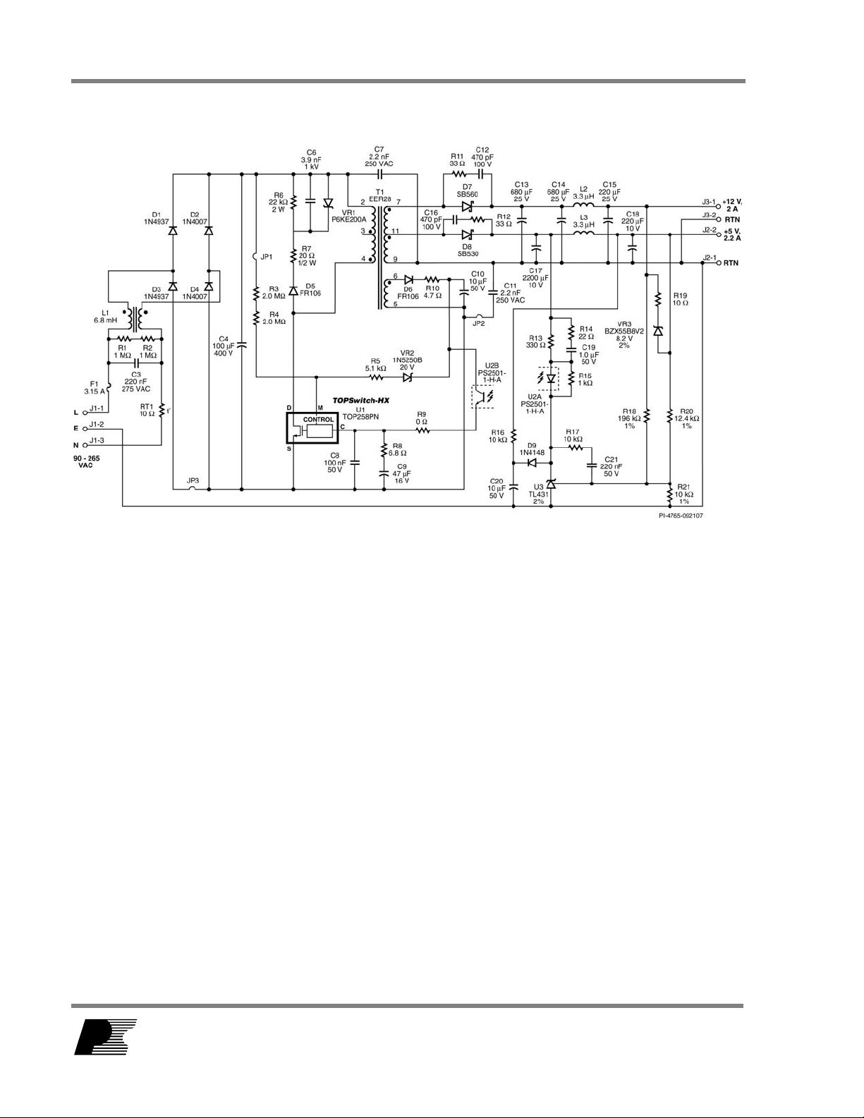
3 Schematic
*
Figure 2 – Schematic.
Optional for 2 wire input, floating output
*
Page 6 of 40
Power Integrations, Inc.
Tel: +1 408 414 9200 Fax: +1 408 414 9201
www.powerint.com

24-Sep-07 RDR-142 35 W, TOP258PN Dual Output Supply
4 Circuit Description
A Flyback converter configuration built around TOP258PN is used in this power supply to
obtain two output voltages. The 5 V output can supply a load current of 2.2 A, and the 12
V output can supply a load current of 2.0 A. This power supply can operate between 90
– 264 VAC. The 5 V output is the main regulated output. This output is regulated using a
TL431 voltage reference. Some feedback is also derived from the 12 V output for
improved cross regulation.
4.1 Input EMI Filtering
The three wire AC supply is connected to the circuit using connector J1. Fuse F1
provides protection against circuit faults and effectively isolates the circuit from the AC
supply source. Thermistor RT1 limits the inrush current drawn by the circuit at start up.
Optional capacitors C1 and C2 are Y capacitors connected from the Line/Neutral to Earth
to reduce common mode EMI.
Capacitor C3 is the X capacitor and helps to reduce the differential mode EMI. Resistors
R1 and R2 discharge C3 on AC removal, preventing potential user shock. Inductor L1 is
a common-mode inductor and helps in filtering common-mode EMI from coupling back to
the AC source.
Diodes D1, D2, D3 and D4 form a bridge rectifier. The bridge rectifier rectifies the
incoming AC supply to DC, which is filtered by capacitor C4.
Diodes D1 and D3 are fast recovery type diodes. These diodes recover very quickly
when the voltage across them reverses. This reduces excitation of stray line inductance
in the AC input by reducing the subsequent high frequency turnoff snap and hence EMI.
Only 2 of the 4 diodes in the bridge need to be fast recovery type, since 2 diodes conduct
in each half cycle.
4.2 TOPSwitch-HX Primary
Resistor R3 and R4 provide line voltage sensing and provide a current to U1, which is
proportional to the DC voltage across capacitor C4. At approximately 95 V DC, the
current through these resistors exceeds the line under-voltage threshold of 25 µA, which
results in enabling of U1.
The TOPSwitch-HX regulates the output using PWM-based voltage mode control. At
high loads the controller operates at full switching frequency (66 kHz for P package
devices). The duty cycle is controlled based on the control pin current to regulate the
output voltage.
The internal current limit provides cycle-by-cycle peak current limit protection. The
TOPSwitch-HX controller has a second current limit comparator allowing monitoring the
actual peak drain current (IP) relative to the programmed current limit I
Page 7 of 40
Tel: +1 408 414 9200 Fax: +1 408 414 9201
Power Integrations
www.powerint.com
LIMITEXT
. As soon

RDR-142 35 W, TOP258PN Dual Output Supply 24-Sep-07
as the ratio IP/I
LIMITEXT
falls below 55%, the peak drain current is held constant. The
output is then regulated by modulating the switching frequency (variable frequency PWM
control). As the load decreases further, the switching frequency decreases linearly from
full frequency down to 30 kHz.
Once the switching frequency has reached 30 kHz the controller keeps this switching
frequency constant and the peak current is reduced to regulate the output (fixed
frequency, direct duty cycle PWM control).
As the load is further reduced and the ratio IP/I
LIMITEXT
falls below 25%, the controller will
enter a multi-cycle-modulation mode for excellent efficiency at light load or standby
operation and low no-load input power consumption.
Diode D5, together with R6, R7, C6 and Zener VR1, forms a clamp network that limits the
drain voltage of U1 at the instant of turn-off. Zener VR1 provides a defined maximum
clamp voltage and typically only conducts during fault conditions such as overload. This
allows the RCD clamp (R6, C6 and D5) to be sized for normal operation, thereby
maximizing efficiency at light load. Resistor R7 is required due to the choice of a fast
recovery diode for D5. A fast versus ultra fast recovery diode allows some recovery of
the clamp energy but requires R7 to limit reverse diode current and dampen high
frequency ringing.
The output of the bias winding is rectified by diode D6 and filtered by resistor R10 and
capacitor C10. This rectified and filtered output is used by the optocoupler U2 to provide
the control current to the control terminal of U1.
Should the feedback circuit fail (open loop condition), the output of the power supply will
exceed the regulation limits. This increased voltage at output will also result in an
increased voltage at the output of the bias winding. Zener VR2 will break down and
current will flow into the “M” pin of IC U1, thus initiating a hysteretic OVP shutdown with
automatic restart attempts. Resistor R5 limits the current into the M pin; if latching OVP
is desired, the value of R5 can be reduced to 20 Ω.
The output voltage of the power supply is maintained in regulation by the feedback circuit
on the secondary side of the circuit. The feedback circuit controls the output voltage by
changing the optocoupler current. Change in the optocoupler diode current results in a
change of current into the control pin of IC U1. Variation of this current results in
variation of duty cycle and hence the output voltage of the power supply.
4.3 Output Rectification
Output rectification for the 5 V output is provided by diode D8. Low ESR capacitor C17
provides filtering. Inductor L3 and capacitor C18 form a second stage filter that
significantly attenuates the switching ripple across C17 and ensures a low ripple output.
Page 8 of 40
Power Integrations, Inc.
Tel: +1 408 414 9200 Fax: +1 408 414 9201
www.powerint.com

24-Sep-07 RDR-142 35 W, TOP258PN Dual Output Supply
Output rectification for the 12 V output is provided by diode D7. Low ESR capacitors C13
and C14 provide filtering. Inductor L2 and capacitor C15 form a second stage filter that
significantly attenuates the switching ripple and ensures low ripple at the output.
Snubber networks comprising R11, C12 and R12, and C16 damp high frequency ringing
across diodes D7 and D8, which results from leakage inductance of the transformer
windings and the secondary trace inductances.
4.4 Output Feedback
Output voltage is controlled using the shunt regulator TL431 (U3). Diode D9, capacitor
C20 and resistor R16 form the soft finish circuit. At start-up, capacitor C20 is discharged.
As the output voltage starts rising, current flows into the optocoupler diode (U2A) via
resistor R13 and diode D9. This provides feedback to the circuit on the primary side.
The current in the optocoupler diode U2A gradually decreases as capacitor C20 charges
and U3 becomes operational. This ensures that the output voltage increases gradually
and settles to the final value without any overshoot. Resistor R16 provides a discharge
path for C20 into the load at power down. Diode D9 isolates C20 from the feedback
circuit after startup.
Resistor R18, R20 and R21 form a voltage divider network that senses the output voltage
from both the outputs for better cross-regulation. Resistor R19 and Zener VR3 improve
cross regulation when only the 5 V output is loaded, which results in the 12 V output
operating at the higher end of the specification.
Resistors R13, R17 and capacitor C21 set the frequency response of the feedback
circuit. Capacitor C19 and resistor R14 form the phase boost network that provides
adequate phase margin to ensure stable operation over the entire operating voltage
range.
Resistor R15 provides the bias current required by the IC U3 and is placed in parallel with
U2A to ensure that the bias current to the IC does not become a part of the feedback
current. Resistor R13 sets the overall DC loop gain and limits the current through U2A
during transient conditions.
Page 9 of 40
Tel: +1 408 414 9200 Fax: +1 408 414 9201
Power Integrations
www.powerint.com
RDR-142 35 W, TOP258PN Dual Output Supply 24-Sep-07
4.5 PCB Layout
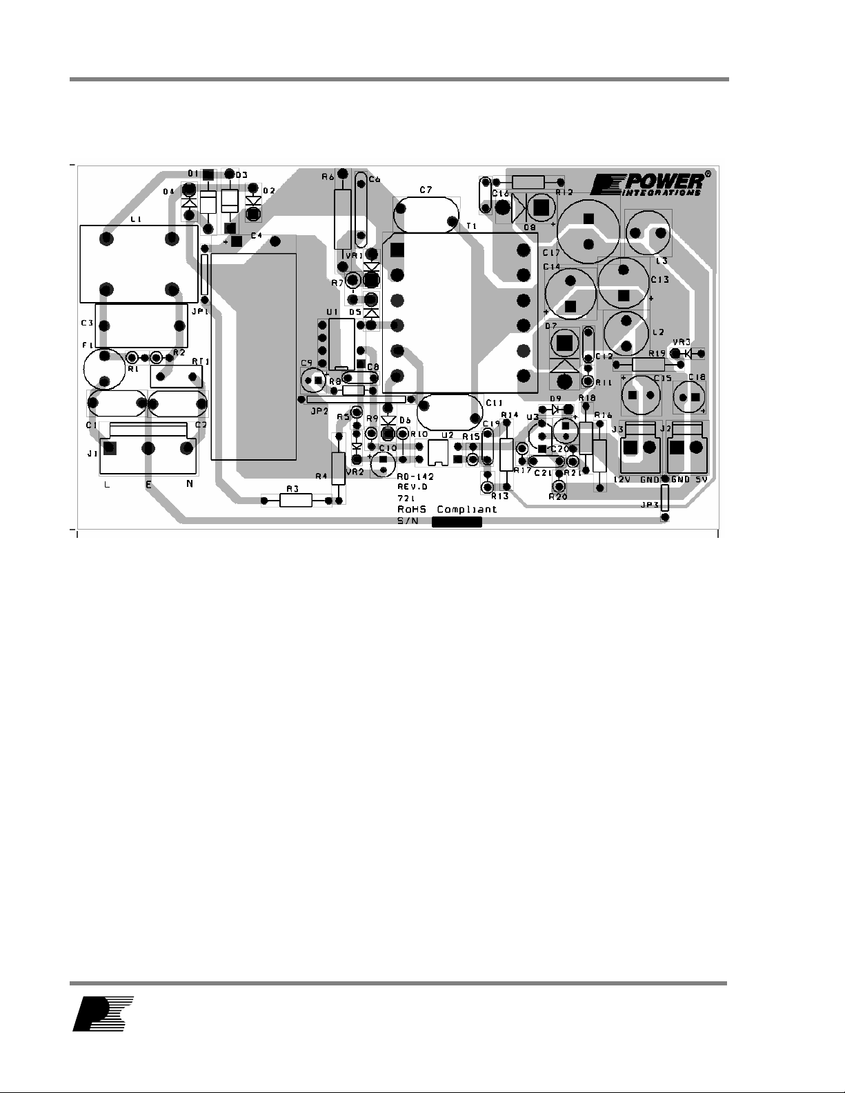
Figure 3 – Printed Circuit Layout.
Page 10 of 40
Power Integrations, Inc.
Tel: +1 408 414 9200 Fax: +1 408 414 9201
www.powerint.com

24-Sep-07 RDR-142 35 W, TOP258PN Dual Output Supply
5 Bill of Materials
Item Qty
1 2
2 1 C3 220 nF, 275 VAC, Film, X2 Panasonic ECQ-U2A224ML
3 1 C4
4 1 C6 3.9 nF, 1 kV, Disc Ceramic, Y5P Panasonic ECK-A3A392KBP
5 2
6 1 C8 100 nF, 50 V, Ceramic, Z5U Kemet C317C104M5U5TA
7 1 C9
8 2
9 2
10 2
11 1 C15
12 1 C17
13 1 C18
14 1 C19 1.0 uF, 50 V, Ceramic, X7R Epcos B37984M5105K000
15 1 C21 220 nF, 50 V, Ceramic, X7R Epcos B37987F5224K000
16 2
17 2
18 2
19 1 D7 60 V, 5 A, Schottky, DO-201AD Vishay SB560
20 1 D8 30 V, 5 A, Schottky, DO-201AD Fairchild SB530
21 1 D9 75 V, 300 mA, Fast Switching, DO-35 Vishay 1N4148
22 1 F1 3.15 A, 250V,Fast, TR5 Wickman 37013150410
23 1 J1 5 Position (1 x 5) header, 0.156 pitch Molex 26-48-1055
24 2 J2 J3 2 Position (1 x 2) header, 0.156 pitch Molex 26-48-1025
25 1 JP1
26 1 JP2
27 1 JP3
28 1 L1 6.8 mH, 0.8 A, Common Mode Choke Panasonic ELF15N008
29 2 L2 L3 3.3 uH, 5.0 A Coilcraft RFB0807-3R3L
30 2
31 2
Ref
Des
C11 2.2 nF, Ceramic, Y1 Vishay 440LD22-R
C10
C20
C12
C16 470 pF, 100 V, Ceramic, COG AVX Corp 5NK471KOBAM
C13
C14
Description Mfg Mfg Part Number
C1
C2
1 nF, Ceramic, Y1 Panasonic ECK-ANA102MB
100 uF, 400 V, Electrolytic, Low ESR,
630 mOhm, (16 x 40)
C7
47 uF, 16 V, Electrolytic, Gen Purpose,
(5 x 11.5) Panasonic ECA-1CHG470
10 uF, 50 V, Electrolytic, Gen Purpose,
(5 x 11)
680 uF, 25 V, Electrolytic, Very Low
ESR, 23 mOhm, (10 x 20)
220 uF, 25 V, Electrolytic, Low ESR,
120 mOhm, (8 x 12)
2200 uF, 10 V, Electrolytic, Very Low
ESR,21 mOhm, (12.5 x 20)
220 uF, 10 V, Electrolytic, Low ESR,
250 mOhm, (6.3 x 11.5)
D1
600 V, 1 A, Fast Recovery Diode,
D3
200 ns, DO-41
D2
D4 1000 V, 1 A, Rectifier, DO-41 Vishay 1N4007
D5
800 V, 1 A, Fast Recovery Diode,
D6
500 ns, DO-41 Diodes Inc. FR106
Wire Jumper, Non insulated,
22 AWG, 0.4 in
Wire Jumper, Non insulated,
22 AWG, 0.8 in Alpha 298
Wire Jumper, Non insulated,
22 AWG, 0.3 in Alpha 298
R1
R2 1 M, 5%, 1/4 W, Carbon Film Yageo CFR-25JB-1M0
R3
R4 2.0 M, 5%, 1/4 W, Carbon Film Yageo CFR-25JB-2M0
Nippon ChemiCon
Panasonic ECA-1HHG100
Nippon ChemiCon EKZE250ELL681MJ20S
Nippon ChemiCon
Nippon ChemiCon EKZE100ELL222MK20S
Nippon ChemiCon ELXZ100ELL221MFB5D
On
Semiconductor 1N4937RLG
Alpha 298
EKMX401ELL101ML40
S
ELXZ250ELL221MH12D
Page 11 of 40
Tel: +1 408 414 9200 Fax: +1 408 414 9201
Power Integrations
www.powerint.com

RDR-142 35 W, TOP258PN Dual Output Supply 24-Sep-07
32 1 R5 5.1 k, 5%, 1/4 W, Carbon Film Yageo CFR-25JB-5K1
33 1 R6 22 k, 5%, 2 W, Metal Oxide Yageo RSF200JB-22K
34 1 R7 20 R, 5%, 1/2 W, Carbon Film Yageo CFR-50JB-20R
35 1 R8 6.8 R, 5%, 1/8 W, Carbon Film Yageo CFR-12JB-6R8
36 1 R9 100 R, 5%, 1/4 W, Carbon Film Yageo CFR-25JB-100R
37 1 R10 4.7 R, 5%, 1/4 W, Carbon Film Yageo CFR-25JB-4R7
R11
38 2
39 1 R13 330 R, 5%, 1/4 W, Carbon Film Yageo CFR-25JB-330R
40 1 R14 22 R, 5%, 1/4 W, Carbon Film Yageo CFR-25JB-22R
41 1 R15 1 k, 5%, 1/4 W, Carbon Film Yageo CFR-25JB-1K0
42 2
43 1 R18 196 k, 1%, 1/4 W, Metal Film Yageo MFR-25FBF-196K
44 1 R19 10 R, 5%, 1/4 W, Carbon Film Yageo CFR-25JB-10R
45 1 R20 12.4 k, 1%, 1/4 W, Metal Film Yageo MFR-25FBF-12K4
46 1 R21 10 k, 1%, 1/4 W, Metal Film Panasonic ERO-S2PHF1002
47 1 RT1 NTC Thermistor, 10 Ohms, 1.7 A Thermometrics CL-120
48 1 T1
49 1 U1 TOPSwitch-HX, TOP258PN, DIP-8B
50 1 U2
51 1 U3
52 1 VR1
53 1 VR2 20 V, 5%, 500 mW, DO-35 Microsemi 1N5250B
54 1 VR3 8.2 V, 500 mW, 2%, DO-35 Vishay BZX55B8V2
R12 33 R, 5%, 1/4 W, Carbon Film Yageo CFR-25JB-33R
R16
R17 10 k, 5%, 1/4 W, Carbon Film Yageo CFR-25JB-10K
Core
Bobbin: EER28, Horiz., 12 pins (6/6),
Complete Assembly (custom)
Opto coupler, 80 V, CTR 80-160%, 4DIP NEC PS2501-1-H-A
2.495 V Shunt Regulator IC, 2%, 0 to
70C, TO-92
200 V, 600 W, 5%, TVS, DO204AC
(DO-15)
TDK
Ying-Chin
Ice Components
Magtel
Precision Inc.
Power
Integrations
On
Semiconductor TL431CLPG
OnSemi P6KE200ARLG
PC40EER28-Z
YC-2806-5
TOP07074
32/07 TR.RDK-142
019-4967-00R
TOP258PN
Note – Parts listed above are RoHS compliant
Page 12 of 40
Power Integrations, Inc.
Tel: +1 408 414 9200 Fax: +1 408 414 9201
www.powerint.com

24-Sep-07 RDR-142 35 W, TOP258PN Dual Output Supply
6 Transformer Specification
6.1 Electrical Diagram
Figure 4 – Transformer Electrical Diagram.
6.2 Electrical Specifications
Electrical Strength
Primary Inductance
Resonant Frequency
Primary Leakage Inductance
1 second, 60 Hz, from Pins 2,3,4,5,6 to Pins 7,9,11 3000 VAC
Pins 2-4, all other windings open, measured at 100
kHz, 0.4 VRMS
Pins 2-4, all other windings open 1000 kHz (Min.)
Pins 2-4, with Pins 7-9 shorted, measured at
100 kHz, 0.4 VRMS
1040 µH, ±10%
20 µH (Max.)
6.3 Materials
Item Description
[1] Core: EER28 gapped for ALG of 213 nH/T
[2] Bobbin: EER28, Horizontal 12 pins (6/6), YC-2806-5
[3] Magnet Wire: #27 AWG, double coated.
[4] Magnet Wire: #26 AWG, double coated.
[5] Tape: 3M Polyester Film, 2.0 mils thick, 16.0 mm wide.
[6] Tape: 3M Polyester Film, 2.0 mils thick, 10.0 mm wide.
[7] Copper Foil, 2 mils thick, 142mm long, 8.5mm wide. To be wrapped over with tape item [6].
[8] Tape: 3M Polyester Film, 2.0 mils thick, 13.5 mm wide.
[9] Bare Wire: #22 AWG
[10] Tape: 3M Polyester Film, 2.0 mils thick, 8.0 mm wide.
[11] Varnish.
2
Page 13 of 40
Tel: +1 408 414 9200 Fax: +1 408 414 9201
Power Integrations
www.powerint.com
RDR-142 35 W, TOP258PN Dual Output Supply 24-Sep-07
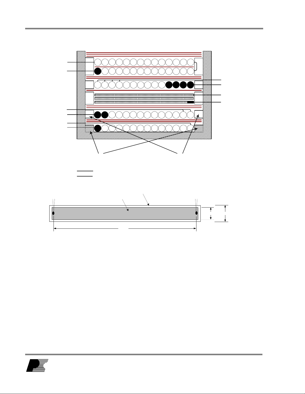
6.4 Transformer Build Diagram
2
3
11
7
9
11
5
6
3
4
2 x #28AWG connected to pin 7
( 3.1 mm pre-molded margin bobbin)
Bobbin: EER28 (Horizontal, 12pins, 6/6), YC-2806-5)
Lp(2-4):
1.04mH +/- 5%
Copper Fo il – 2mil thick
142mm
Figure 5 – Transformer Build Diagram.
margin tape
Tape: 3M Polyester Film – 2mil thick
2 x #28AWG connected to pin 11
8.5mm
13.5mm
Page 14 of 40
Power Integrations, Inc.
Tel: +1 408 414 9200 Fax: +1 408 414 9201
www.powerint.com

24-Sep-07 RDR-142 35 W, TOP258PN Dual Output Supply
6.5 Transformer Construction
General Note
Primary side of the bobbin orients to the left hand side. Place 3.1 mm margin tape
on both sides for all windings except WD1 due to built-in 3.1 mm margin of bobbin.
Winding direction is clockwise.
1/2 Primary
Insulation
Insulation
st
Secondary
1
Insulation
nd
2
Secondary
Insulation
2/2 Primary
Insulation
Assembly
WD1
WD2
Bias
WD3
WD4
WD5
Finish
Start on pin 4, wind 24 turns of item [3] from left to right with tight tension and bring
the wire across the bobbin to terminate at pin 3.
2 layers of tape item [5].
Start on pin 6, wind 7 turns bifilar of item [4] from left to right, spread the winding
evenly, and bring the wire across the bobbin to terminate on pin 5.
2 layers of tape item [5].
Start on pin 11, wind 3 turns of item [7] and terminate at pin 9.
1 layer of tape item [5].
Start on pin 7, wind 4 turns quadfilar of item [4] from right to left, spread the winding
evenly across the bobbin, and bring the wire back to the right to terminate on pin11.
2 layers of tape item [5].
Start on pin 3, wind 23 turns of item [3] from left to right with tight tension, place 1
layer tape item [6], then wind another 23 turns of item [3] from right to left, also with
tight tension, and terminate at pin 2.
3 layers of tape item [5].
Grind the cores to get 1038 µH with ALG of 213 nH/T
Secure the cores by wrapping around 2 halves of cores with item [10]. Dip varnish
uniformly in item [11]
.
2
Page 15 of 40
Tel: +1 408 414 9200 Fax: +1 408 414 9201
Power Integrations
www.powerint.com

RDR-142 35 W, TOP258PN Dual Output Supply 24-Sep-07
7 Design Spreadsheet
ACDC_TOPSwitchHX_09
0607; Rev.1.2; Copyright
Power Integrations 2007
ENTER APPLICATION VARIABLES RD-142
VACMIN 90 Volts Minimum AC Input Voltage
VACMAX 265 Volts Maximum AC Input Voltage
fL 50 Hertz AC Mains Frequency
VO 5.00
PO_AVG 35.00
PO_PEAK 35.00 Watts Peak Output Power
n 0.80 %/100 Efficiency Estimate
Z 0.50 Loss Allocation Factor
VB 12
tC 3.00 mSeco
CIN 100.0 100 uFara
ENTER TOPSWITCH-HX VARIABLES
TOPSwitch-HX TOP258PN Univer
Chosen Device
KI 1.00
ILIMITMIN_EXT 1.534 Amps Use 1% resistor in setting external ILIMIT
ILIMITMAX_EXT 1.766 Amps Use 1% resistor in setting external ILIMIT
Frequency (F)=132kHz,
(H)=66kHz
fS
fSmin
fSmax
High Line Operating Mode FF
VOR 128.00 Volts Reflected Output Voltage
VDS 5.63 5.63 Volts TOPSwitch on-state Drain to Source Voltage
VD 0.50 Volts Output Winding Diode Forward Voltage Drop
VDB 0.70 Volts Bias Winding Diode Forward Voltage Drop
KP 0.69
INPUT INFO
Info
TOP258PN
H
66000 Hertz TOPSwitch-HX Switching Frequency: Choose
OUTPU
T
Volts Output Voltage (main)
Watts Average Output Power
Volts Ensure proper operation at no load.
Power
Out
H Only half frequency option available for P, G
59400 Hertz TOPSwitch-HX Minimum Switching Frequency
72600 Hertz TOPSwitch-HX Maximum Switching Frequency
Ripple to Peak Current Ratio (0.3 < KRP < 1.0
UNIT
nds
ds
sal /
Peak
35 W /
50 W
External Ilimit reduction factor (KI=1.0 for
TOPSwitch_HX_090607: TOPSwitch-HX
Continuous/Discontinuous Flyback
Transformer Design Spreadsheet
Bridge Rectifier Conduction Time Estimate
Input Filter Capacitor
115 Doubled/230V
48W
default ILIMIT, KI <1.0 for lower ILIMIT)
and M package devices. For full frequency
operation choose Y package.
between 132 kHz and 66 kHz
: 1.0< KDP<6.0)
Page 16 of 40
Power Integrations, Inc.
Tel: +1 408 414 9200 Fax: +1 408 414 9201
www.powerint.com

24-Sep-07 RDR-142 35 W, TOP258PN Dual Output Supply
PROTECTION FEATURES
LINE SENSING Note - For P/G package devices only one of
VUV_STARTUP 95.00 95 Volts DC Bus Voltage at which the power supply will
VOV_SHUTDOWN 445 Volts DC Bus Voltage at which power supply will
RLS 4.0 MOUTPUT OVERVOLTAGE
VZ 22 Volts Zener Diode rated voltage for Output
RZ 5.1 kOVERLOAD POWER LIMITING
Overload Current Ratio at VMAX 1.2 Enter the desired margin to current limit at
Overload Current Ratio at VMIN
ILIMIT_EXT_VMIN 1.23 A External Current limit at VMIN
ILIMIT_EXT_VMAX 1.14 A External Current limit at VMAX
RIL 8.29 k-
RPL 29.27 M-
ENTER TRANSFORMER CORE/CONSTRUCTION VARIABLES
Core Type EER28 EER28 Core Type
Core
Bobbin
AE 0.821 cm^2 Core Effective Cross Sectional Area
LE 6.4 cm Core Effective Path Length
AL 2870 nH/T^2 Ungapped Core Effective Inductance
EER28_BO
EER28
1.25 Margin to current limit at low line.
BBIN
ohms
ohms
ohms
ohms
P/N:
P/N:
either Line sensing or Overload power limiting
protection featues can be used. For all other
packages both these functions can be
simultaneously used.
start-up
shut-down
Use two standard, 2 M-Ohm, 5% resistors in
series for line sense functionality.
Overvoltage shutdown protection
Output OVP resistor. For latching shutdown
use 20 ohm resistor instead
VMAX. A value of 1.2 indicates that the current
limit should be 20% higher than peak primary
current at VMAX
Current limit/Power Limiting resistor.
Power Limiting resistor
PC40EER28-Z
BW 16.7 mm Bobbin Physical Winding Width
M 3.00 mm Safety Margin Width (Half the Primary to
L 3.00 Number of Primary Layers
NS 3 3 Number of Secondary Turns
DC INPUT VOLTAGE PARAMETERS
VMIN 100 Volts Minimum DC Input Voltage
VMAX 375 Volts Maximum DC Input Voltage
CURRENT WAVEFORM SHAPE PARAMETERS
DMAX
IAVG 0.44 Amps Average Primary Current (calculated at
IP 1.16 Amps Peak Primary Current (calculated at Peak
IR 0.80 Amps Primary Ripple Current (calculated at average
IRMS 0.60 Amps Primary RMS Current (calculated at average
0.57 Maximum Duty Cycle (calculated at PO_PEAK)
Tel: +1 408 414 9200 Fax: +1 408 414 9201
Page 17 of 40
Secondary Creepage Distance)
average output power)
output power)
output power)
output power)
Power Integrations
www.powerint.com

RDR-142 35 W, TOP258PN Dual Output Supply 24-Sep-07
TRANSFORMER PRIMARY DESIGN PARAMETERS
LP 1040 uHenries Primary Inductance
LP Tolerance 10 Tolerance of Primary Inductance
NP 70 Primary Winding Number of Turns
NB 7 Bias Winding Number of Turns
ALG 213 nH/T^2 Gapped Core Effective Inductance
BM 2101 Gauss Maximum Flux Density at PO, VMIN
BP 3524 Gauss Peak Flux Density (BP<4200) at ILIMITMAX
BAC 725 Gauss AC Flux Density for Core Loss Curves (0.5 X
ur 1780 Relative Permeability of Ungapped Core
LG
BWE 32.1 mm Effective Bobbin Width
OD 0.46 mm Maximum Primary Wire Diameter including
INS 0.06 mm Estimated Total Insulation Thickness (= 2 * film
DIA 0.40 mm Bare conductor diameter
AWG 27 AWG Primary Wire Gauge (Rounded to next smaller
CM 203 Cmils Bare conductor effective area in circular mils
CMA
Primary Current Density (J) 5.88 Amps/m
TRANSFORMER SECONDARY DESIGN PARAMETERS (SINGLE OUTPUT EQUIVALENT)
Lumped parameters
ISP 26.95 Amps Peak Secondary Current
ISRMS 12.03 Amps Secondary RMS Current
IO_PEAK 7.00 Amps Secondary Peak Output Current
IO 7.00 Amps Average Power Supply Output Current
IRIPPLE 9.79 Amps Output Capacitor RMS Ripple Current
CMS 2407 Cmils Secondary Bare Conductor minimum circular
AWGS 16 AWG Secondary Wire Gauge (Rounded up to next
DIAS 1.29 mm Secondary Minimum Bare Conductor Diameter
ODS 3.57 mm Secondary Maximum Outside Diameter for
INSS 1.14 mm Maximum Secondary Insulation Wall Thickness
VOLTAGE STRESS PARAMETERS
VDRAIN 625 Volts Maximum Drain Voltage Estimate (Includes
PIVS 21 Volts Output Rectifier Maximum Peak Inverse
PIVB 49 Volts Bias Rectifier Maximum Peak Inverse Voltage
0.45 mm Gap Length (Lg > 0.1 mm)
338 Cmils/A
mp
m^2
(BM<3000)
and LP_MAX. Note: Recommended values for
adapters and external power supplies <=3600
Gauss
Peak to Peak)
insulation
thickness)
standard AWG value)
Primary Winding Current Capacity (200 < CMA
< 500)
Primary Winding Current density (3.8 < J <
9.75)
mils
larger standard AWG value)
Triple Insulated Wire
Effect of Leakage Inductance)
Voltage
Page 18 of 40
Power Integrations, Inc.
Tel: +1 408 414 9200 Fax: +1 408 414 9201
www.powerint.com

24-Sep-07 RDR-142 35 W, TOP258PN Dual Output Supply
TRANSFORMER SECONDARY DESIGN PARAMETERS (MULTIPLE OUTPUTS)
1st output
VO1 5.00
IO1_AVG 2.20 2.2 Amps Average DC Output Current
PO1_AVG 11.00 Watts Average Output Power
VD1 0.5 Volts Output Diode Forward Voltage Drop
NS1 3.00 Output Winding Number of Turns
ISRMS1 3.782 Amps Output Winding RMS Current
IRIPPLE1 3.08 Amps Output Capacitor RMS Ripple Current
PIVS1 21 Volts Output Rectifier Maximum Peak Inverse
CMS1 756 Cmils Output Winding Bare Conductor minimum
AWGS1 21 AWG Wire Gauge (Rounded up to next larger
DIAS1 0.73 mm Minimum Bare Conductor Diameter
ODS1 3.57 mm Maximum Outside Diameter for Triple Insulated
2nd output
VO2 12.00
IO2_AVG 2.00 Amps Average DC Output Current
PO2_AVG 24.00 Watts Average Output Power
VD2 0.7 Volts Output Diode Forward Voltage Drop
NS2 6.93 Output Winding Number of Turns
ISRMS2 3.438 Amps Output Winding RMS Current
IRIPPLE2 2.80 Amps Output Capacitor RMS Ripple Current
PIVS2 49 Volts Output Rectifier Maximum Peak Inverse
CMS2 688 Cmils Output Winding Bare Conductor minimum
AWGS2 21 AWG Wire Gauge (Rounded up to next larger
DIAS2 0.73 mm Minimum Bare Conductor Diameter
ODS2 1.54 mm Maximum Outside Diameter for Triple Insulated
3rd output
VO3
IO3_AVG Amps Average DC Output Current
PO3_AVG 0.00 Watts Average Output Power
VD3 0.7 Volts Output Diode Forward Voltage Drop
NS3 0.38 Output Winding Number of Turns
ISRMS3 0.000 Amps Output Winding RMS Current
IRIPPLE3 0.00 Amps Output Capacitor RMS Ripple Current
PIVS3 2 Volts Output Rectifier Maximum Peak Inverse
CMS3 0 Cmils Output Winding Bare Conductor minimum
AWGS3 N/A AWG Wire Gauge (Rounded up to next larger
DIAS3 N/A mm Minimum Bare Conductor Diameter
ODS3 N/A mm Maximum Outside Diameter for Triple Insulated
Total Continuous Output Power
Negative Output N/A If negative output exists enter Output number;
5 Volts Output Voltage
Voltage
circular mils
standard AWG value)
Wire
Volts Output Voltage
Voltage
circular mils
standard AWG value)
Wire
Volts Output Voltage
Voltage
circular mils
standard AWG value)
Wire
35 Watts Total Continuous Output Power
eg: If VO2 is negative output, enter 2
Page 19 of 40
Tel: +1 408 414 9200 Fax: +1 408 414 9201
Power Integrations
www.powerint.com
RDR-142 35 W, TOP258PN Dual Output Supply 24-Sep-07
8 Performance Data
All measurements performed at room temperature, 60 Hz input frequency.
8.1 Efficiency
Efficiency
84.5%
84.0%
83.5%
83.0%
82.5%
82.0%
81.5%
Efficiency (%)
81.0%
80.5%
80.0%
20.0% 40.0% 60.0% 80.0% 100.0%
115 VAC
230 VAC
Load (A)
Figure 6 – Efficiency vs. Input Voltage, Room Temperature, 60 Hz.
8.1.1 Active Mode CEC Measurement Data
All single output adapters, including those provided with products, for sale in California
st
after Jan 1
, 2008 must meet the California Energy Commission (CEC) requirement for
minimum active mode efficiency and no load input power. Minimum active mode
efficiency is defined as the average efficiency of 25, 50, 75 and 100% of rated output
power with the limit based on the nameplate output power:
Nameplate Output (PO) Minimum Efficiency in Active Mode of Operation
< 1 W
≥ 1 W to ≤ 49 W 0.09 × ln (PO) + 0.5 [ln = natural log]
> 49 W 0.85
0.49 × P
O
For adapters that are single input voltage only, then the measurement is made at the
rated single nominal input voltage (115 VAC or 230 VAC); for universal input adapters the
measurement is made at both nominal input voltages (115 VAC and 230 VAC).
Page 20 of 40
Power Integrations, Inc.
Tel: +1 408 414 9200 Fax: +1 408 414 9201
www.powerint.com

24-Sep-07 RDR-142 35 W, TOP258PN Dual Output Supply
To meet the standar, the measured average efficiency (or efficiencies for universal input
supplies) must be greater than or equal to the efficiency specified by the CEC/Energy
Star standard.
Percent of
Full Load
25 80.6 80.5
50 82.7 83.7
75 83.0 83.9
100 82.7 84.0
Average 82.2 83.0
CEC
specified
minimum
average
efficiency (%)
Efficiency (%)
115 VAC 230 VAC
82.0*
*Although the CEC standard does not apply to this design, the data is provided for
reference
More states within the USA and other countries are adopting this standard, for the latest
up to date information please visit the PI Green Room:
http://www.powerint.com/greenroom/regulations.htm
Page 21 of 40
Tel: +1 408 414 9200 Fax: +1 408 414 9201
Power Integrations
www.powerint.com

RDR-142 35 W, TOP258PN Dual Output Supply 24-Sep-07
8.2 No-load Input Power
No-Load Input Power
0.260
0.240
0.220
0.200
0.180
Input Power (W)
0.160
0.140
85 105 125 145 165 185 205 225 245 265
AC Input (VAC)
Figure 7 – Zero Load Input Power vs. Input Line Voltage, Room Temperature, 60 Hz.
Page 22 of 40
Power Integrations, Inc.
Tel: +1 408 414 9200 Fax: +1 408 414 9201
www.powerint.com
24-Sep-07 RDR-142 35 W, TOP258PN Dual Output Supply
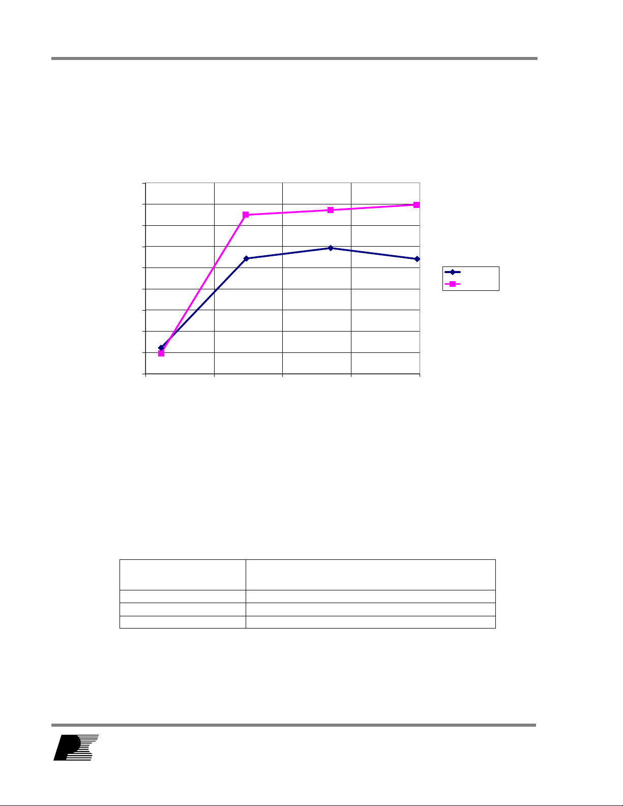
8.3 Available Standby Output Power
The chart below shows the available output power vs line voltage for an input power of 1
W, 2 W and 3 W. This measurement was taken by loading the 5 Volt output.
Available Output Power
1.800
1.600
1.400
1.200
1 W Input Power
1.000
0.800
Output Power (W)
0.600
2 W Input Power
3 W Input Power
0.400
0.200
85 105 125 145 165 185 205 225 245 265
Input Voltage (VAC)
Figure 8 – Available Standby Output Power for Fixed Levels of Input Power
Page 23 of 40
Tel: +1 408 414 9200 Fax: +1 408 414 9201
Power Integrations
www.powerint.com

RDR-142 35 W, TOP258PN Dual Output Supply 24-Sep-07
p
)
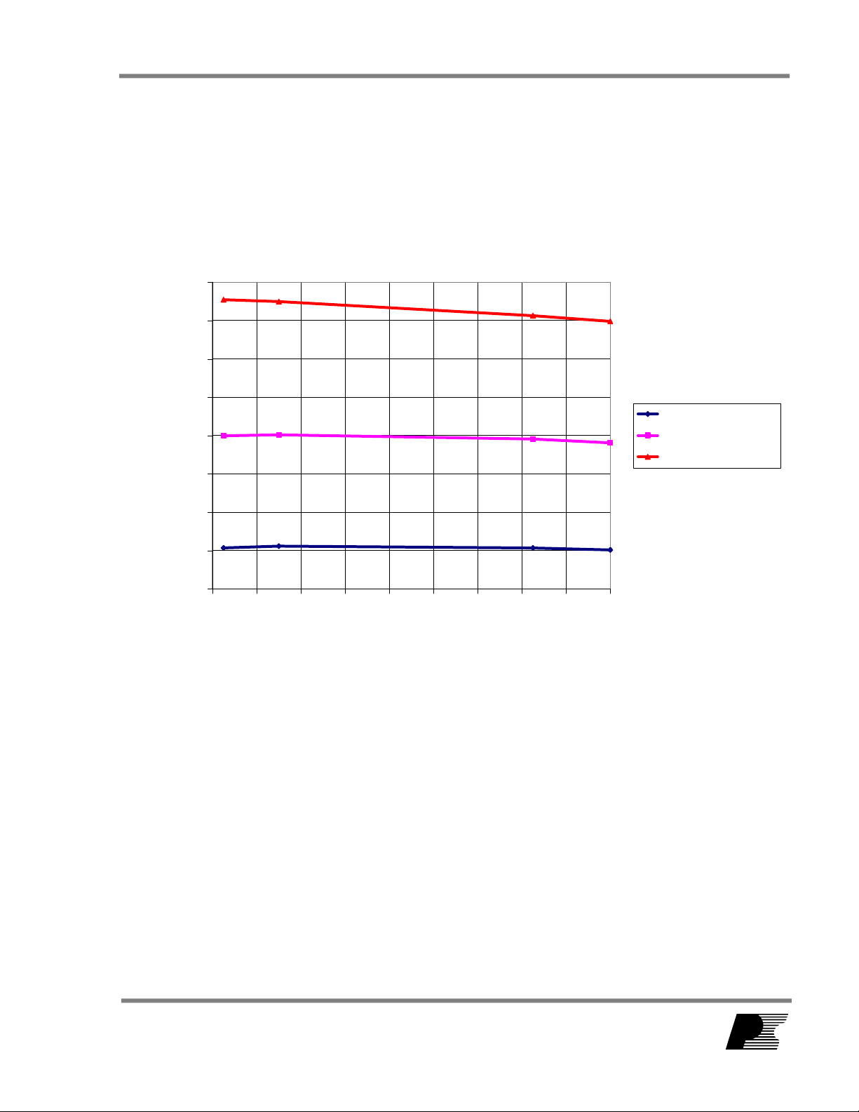
9 Regulation
9.1.1 Load
Load Regulation
13.0
12.0
11.0
10.0
9.0
8.0
7.0
Output Voltage (V)
6.0
5.0
4.0
0 5 10 15 20 25 30 35
5 V Output, 115 VAC
5 V Output, 230 VAC
12 V Output, 115 VAC
12 V Output, 230 VAC
Out
ut Power (W
Figure 9 – Load Regulation, Room Temperature
Page 24 of 40
Power Integrations, Inc.
Tel: +1 408 414 9200 Fax: +1 408 414 9201
www.powerint.com

24-Sep-07 RDR-142 35 W, TOP258PN Dual Output Supply
9.1.2 Line
Line Regulation
13.00
12.00
11.00
10.00
9.00
8.00
7.00
Output Voltage (V)
6.00
5.00
4.00
5 V Output
12 V Output
85 135 185 235
AC Input (VAC)
Figure 10 – Line Regulation, Room Temperature, Full Load
Page 25 of 40
Tel: +1 408 414 9200 Fax: +1 408 414 9201
Power Integrations
www.powerint.com

RDR-142 35 W, TOP258PN Dual Output Supply 24-Sep-07
9.1.3 Cross Regulation Matrix
The table below shows the data for the outputs under various loading conditions at 90
and 265 VAC. The regulation on the 5 V output was within ±5% under all conditions.
90 VAC constant 50 mA load on 12 V 265 VAC constant 50 mA load on 12 V
IO (12 V) IO (5 V) VO (5 V) VO (12 V) IO (12 V) IO (5 V) VO (5 V) VO (12 V)
0.05 0.05 4.96 12.23 0.05 0.05 4.95 12.27
0.05 0.5 4.9 13.12 0.05 0.5 4.89 13.2
0.05 1 4.85 13.82 0.05 1 4.85 13.95
0.05 1.5 4.82 14.4 0.05 1.5 4.8 14.64
0.05 2.2 4.79 14.9 0.05 2.2 4.78 14.98
90 VAC - 12 V held constant at full load 265 VAC - 12 V held constant at full load
IO (12 V) IO (5 V) VO (5 V) VO (12 V) IO (12 V) IO (5 V) VO (5 V) VO (12 V)
2 0.05 4.99 11.7 2 0.05 4.99 11.66
2 0.5 4.97 12 2 0.5 4.97 11.97
2 1 4.96 12.14 2 1 4.96 12.1
2 1.5 4.95 12.27 2 1.5 4.95 12.22
2 2.2 4.94 12.4 2 2.2 4.94 12.33
90 VAC constant 50 mA load on 5 V 265 VAC constant 50 mA load on 5 V
IO (5 V) IO (12 V) VO (12 V) VO (5 V) IO (5 V) IO (12 V) VO (12 V) VO (5 V)
0.05 0.05 12.26 4.95 0.05 0.05 12.27 4.95
0.05 0.5 11.91 4.97 0.05 0.5 11.91 4.99
0.05 1 11.79 4.98 0.05 1 11.76 4.99
0.05 1.5 11.73 4.98 0.05 1.5 11.69 4.99
0.05 2 11.68 4.98 0.05 2 11.63 4.99
90 VAC constant 2.2 A load on 5 V 265 VAC constant 2.2 A load on 5 V
IO (5 V) IO (12 V) VO (12 V) VO (5 V) IO (5 V) IO (12 V) VO (12 V) VO (5 V)
2.2 0.05 14.96 4.78 2.2 0.05 14.87 4.8
2.2 0.5 12.91 4.91 2.2 0.5 12.96 4.91
2.2 1 12.54 4.94 2.2 1 12.55 4.93
2.2 1.5 12.42 4.94 2.2 1.5 12.98 4.94
2.2 2 12.36 4.94 2.2 2 12.32 4.94
Table 1 : Cross regulation data under various loading conditions
Page 26 of 40
Power Integrations, Inc.
Tel: +1 408 414 9200 Fax: +1 408 414 9201
www.powerint.com

24-Sep-07 RDR-142 35 W, TOP258PN Dual Output Supply
10 Thermal Performance
Measurements were taken with no air flow across the power supply.
Item
Ambient
Output Capacitor (C17)
Transformer (T1)
Clamp Diode
TOPSwitch (U1)
Source pin
Rectifier (D8)
Table 2 – Thermal Performance, Full Load
Temperature (°C)
90 VAC 265 VAC
50 51
71 61
87 87
96 91
108 91
89 88
Figure 11 – Infrared Thermograph of Open Frame Operation, at Room Temperature
Page 27 of 40
90 VAC, 35 W load, 21ºC Ambient
Tel: +1 408 414 9200 Fax: +1 408 414 9201
Power Integrations
www.powerint.com

RDR-142 35 W, TOP258PN Dual Output Supply 24-Sep-07
11 Waveforms
11.1 Drain Voltage and Current, Normal Operation
Figure 12 – 90 VAC, Full Load.
Upper: V
Lower: I
, 100 V, 5 µs / div
DRAIN
, 0.5 A / div
DRAIN
11.2 Output Voltage Start-up Profile
Figure 14 – 5 Volt Start-up Profile, Full load;
90 VAC; 1 V/div, 5 ms / div.
Figure 13 – 265 VAC, Full Load
Upper: V
Lower: I
, 200 V, 5 µs / div
DRAIN
, 0.5 A / div
DRAIN
Figure 15 – 5 Volt Start-up Profile, Full load; 265
VAC; 1 V/div, 5 ms / div.
Page 28 of 40
Power Integrations, Inc.
Tel: +1 408 414 9200 Fax: +1 408 414 9201
www.powerint.com

24-Sep-07 RDR-142 35 W, TOP258PN Dual Output Supply
Figure 16 – 12 Volt Start-up Profile, Full load;
90 VAC; 2 V/div, 5 ms / div
Figure 17 – 12 Volt Start-up Profile, Full load;
265 VAC; 2 V/div, 5 ms / div.
Page 29 of 40
Tel: +1 408 414 9200 Fax: +1 408 414 9201
Power Integrations
www.powerint.com

RDR-142 35 W, TOP258PN Dual Output Supply 24-Sep-07
11.3 Drain Voltage and Current Start-up Profile
Figure 18 – 90 VAC Input and Maximum Load.
Upper: V
Lower: I
, 100 V, 2 mS / div
DRAIN
, 0.5 A / div.
DRAIN
Figure 19 – 265 VAC Input and Maximum Load.
Upper: V
Lower: I
, 200 V, 2 mS / div
DRAIN
, 0.5 A / div.
DRAIN
Page 30 of 40
Power Integrations, Inc.
Tel: +1 408 414 9200 Fax: +1 408 414 9201
www.powerint.com
24-Sep-07 RDR-142 35 W, TOP258PN Dual Output Supply
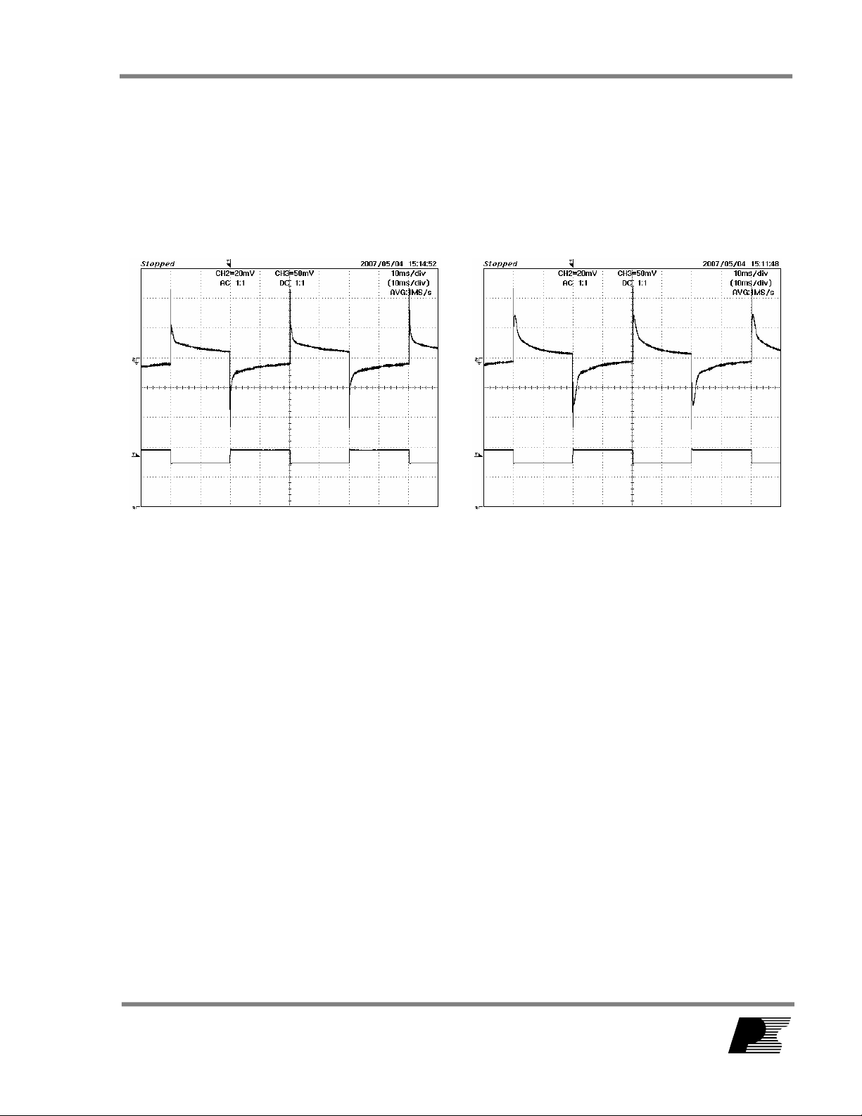
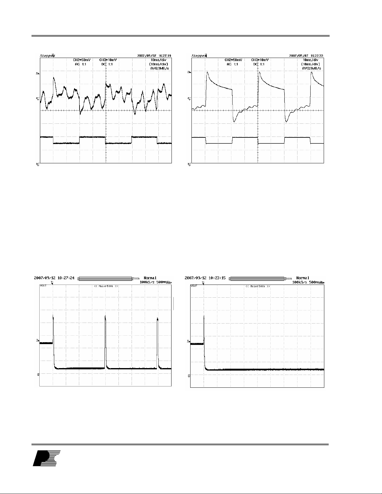
11.4 Load Transient Response (75% to 100% Load Step)
In the figures shown below, signal averaging was used to better enable viewing of the
load transient response. The oscilloscope was triggered using the load current step as a
trigger source. Since the output switching and line frequency occur essentially at random
with respect to the load transient, contributions to the output ripple from these sources
will average out, leaving the contribution only from the load step response.
Figure 20 – 5 Volt Transient Response, 90 VAC,
75-100-75% Load Step.
Output Voltage 20 mV/div, Output
Current 1 A / div, 10 ms / div.
Note
: 12 volt output maintained at full load
Figure 21 – 5 Volt Transient Response, 265 VAC,
75-100-75% Load Step
Output Voltage 20 mV/div, Output
Current 1 A / div, 10 ms / div.
Note
: 12 volt output maintained at full load
Page 31 of 40
Tel: +1 408 414 9200 Fax: +1 408 414 9201
Power Integrations
www.powerint.com
RDR-142 35 W, TOP258PN Dual Output Supply 24-Sep-07
Figure 22 –12 Volt output in response to 5 V
transient, 90 VAC, 75-100-75% Load
Step
Output Voltage 50 mV/div, Output
Current 1 A / div, 10 ms / div.
Figure 23 – 12 Volt output in response to 5 V
transient, 265 VAC, 75-100-75%
Load Step
Output Voltage 50 mV/div, Output
Current 1 A / div, 10 ms / div.
Note: 5 volt output maintained at full load
(Waveshape is combination of line ripple and
transient response - see figure 26)
Note: 5 volt output maintained at full load
11.5 Output Over-voltage Protection
The figures below show the performance of the output over-voltage protection circuit
when the control loop was opened.
Figure 24 –5 Volt output in response to open loop
R5 = 5.1 kΩ to configure hysteretic
shutdown.
Output Voltage 2 V/div, 1 s / div.
Figure 25 –5 Volt output in response to open loop
R5 = 20 Ω to configure latching
shutdown.
Output Voltage 2 V/div, 1 s / div.
Note: 12 V volt output maintained at no load
Page 32 of 40
Power Integrations, Inc.
Tel: +1 408 414 9200 Fax: +1 408 414 9201
www.powerint.com
Note: 12 V volt output maintained at no load

24-Sep-07 RDR-142 35 W, TOP258PN Dual Output Supply
11.6 Output Ripple Measurements
11.6.1 Ripple Measurement Technique
For DC output ripple measurements, a modified oscilloscope test probe must be utilized
in order to reduce spurious signals due to pickup. Details of the probe modification are
provided below.
The 4987BA probe adapter is affixed with two capacitors tied in parallel across the probe
tip. The capacitors include one (1) 0.1 µF/50 V ceramic type and one (1) 1.0 µF/50 V
aluminum electrolytic. The aluminum electrolytic type capacitor is polarized, so proper
polarity across DC outputs must be maintained (see below).
Probe Ground
Probe Tip
Figure 23 – Oscilloscope Probe Prepared for Ripple Measurement. (End Cap and Ground Lead Removed)
Figure 24 – Oscilloscope Probe with Probe Master (www.probemaster.com) 4987A BNC Adapter.
(Modified with wires for ripple measurement, and two parallel decoupling capacitors added)
Page 33 of 40
Tel: +1 408 414 9200 Fax: +1 408 414 9201
Power Integrations
www.powerint.com
RDR-142 35 W, TOP258PN Dual Output Supply 24-Sep-07
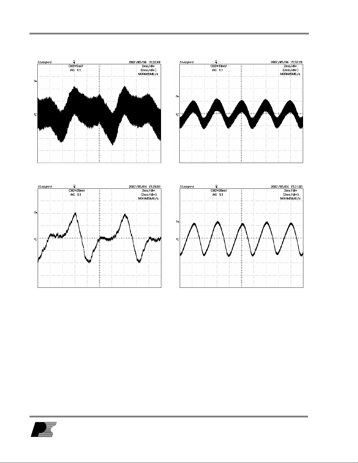
11.6.2 Measurement Results
Figure 26 – 5 V Ripple, 90 VAC, Full Load.
2 ms, 5 mV / div
Figure 28 – 12 V Ripple, 90 VAC, Full Load.
2 ms, 20 mV /div
Figure 27 – 5 V Ripple, 115 VAC, Full Load.
2 ms, 10 mV / div
Figure 29– 12 V Ripple, 115 VAC, Full Load.
2 ms, 20 mV /div
Page 34 of 40
Power Integrations, Inc.
Tel: +1 408 414 9200 Fax: +1 408 414 9201
www.powerint.com

24-Sep-07 RDR-142 35 W, TOP258PN Dual Output Supply
12 Line Surge
Differential input line 1.2/50 µs surge testing was completed on a single test unit to
IEC61000-4-5. Input voltage was set at 230 VAC / 60 Hz. Output was loaded at full load
and operation was verified following each surge event.
Surge
Level (V)
+500 230 L to N 90 Pass
-500 230 L to N 270 Pass
+1000 230 L to N 90 Pass
-1000 230 L to N 270 Pass
+2000 230 L,N to G 90 Pass
-2000 230 L,N to G 270 Pass
Note: Unit passes under all test conditions.
Use a Slow Blow fuse at the input (F1) to increase differential surge withstand to 2 kV
Input
Voltage
(VAC)
Injection
Location
Injection
Phase (°)
Test Result
(Pass/Fail)
Page 35 of 40
Tel: +1 408 414 9200 Fax: +1 408 414 9201
Power Integrations
www.powerint.com
RDR-142 35 W, TOP258PN Dual Output Supply 24-Sep-07
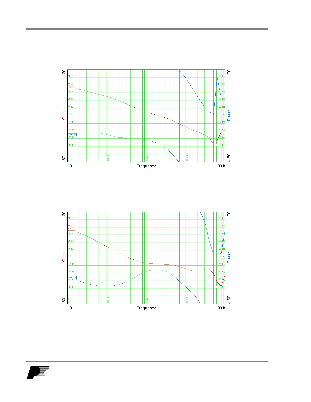
13 Control Loop Measurements
13.1 90 VAC Maximum Load
Figure 30 – Gain-Phase Plot, 90 VAC, Maximum Steady State Load
Vertical Scale: Gain = 10 dB/div, Phase = 30 °/div.
Crossover Frequency = 2.0 kHz Phase Margin = 65°
13.2 265 VAC Maximum Load
Figure 31 – Gain-Phase Plot, 265 VAC, Maximum Steady State Load
Vertical Scale: Gain = 10 dB/div, Phase = 30 °/div.
Crossover Frequency = 350 Hz, Phase Margin = 90°
Page 36 of 40
Power Integrations, Inc.
Tel: +1 408 414 9200 Fax: +1 408 414 9201
www.powerint.com

24-Sep-07 RDR-142 35 W, TOP258PN Dual Output Supply
14 Conducted EMI
Conducted EMI measurements were made with the output connected to the earth ground
connection on the LISN. The result below represents the worst case results.
Figure 32 – Conducted EMI, Neutral Conductor, Maximum Steady State Load, 230 VAC, 60 Hz, and
EN55022 B Limits.
Page 37 of 40
Tel: +1 408 414 9200 Fax: +1 408 414 9201
Power Integrations
www.powerint.com

RDR-142 35 W, TOP258PN Dual Output Supply 24-Sep-07
15 Revision History
Date Author Revision Description & changes Reviewed
24-Sep-07 SGK 1.0 Initial Release
Page 38 of 40
Power Integrations, Inc.
Tel: +1 408 414 9200 Fax: +1 408 414 9201
www.powerint.com

24-Sep-07 RDR-142 35 W, TOP258PN Dual Output Supply
For the latest updates, visit our website: www.powerint.com
Power Integrations reserves the right to make changes to its products at any time to improve reliability or manufacturability. Power
Integrations does not assume any liability arising from the use of any device or circuit described herein. POWER INTEGRATIONS
MAKES NO WARRANTY HEREIN AND SPECIFICALLY DISCLAIMS ALL WARRANTIES INCLUDING, WITHOUT
LIMITATION, THE IMPLIED WARRANTIES OF MERCHANTABILITY, FITNESS FOR A PARTICULAR PURPOSE, AND
NON-INFRINGEMENT OF THIRD PARTY RIGHTS.
PATENT INFORMATION
The products and applications illustrated herein (including transformer construction and circuits external to the products)
may be covered by one or more U.S. and foreign patents, or potentially by pending U.S. and foreign patent applications
assigned to Power Integrations. A complete list of Power Integrations’ patents may be found at www.powerint.com
.
Power Integrations grants its customers a license under certain patent rights as set forth at
http://www.powerint.com/ip.htm.
The PI Logo, TOPSwitch, TinySwitch, LinkSwitch, DPA-Switch, PeakSwitch, EcoSmart, Clampless, E-Shield, Filterfuse, PI Expert and PI FACTS
are trademarks of Power Integrations, Inc. Other trademarks are property of their respective companies. ©Copyright 2006 Power
Integrations, Inc.
Power Integrations Worldwide Sales Support Locations
WORLD HEADQUARTERS
5245 Hellyer Avenue
San Jose, CA 95138, USA.
Main: +1-408-414-9200
Customer Service:
Phone: +1-408-414-9665
Fax: +1-408-414-9765
e-mail: usasales@powerint.com
CHINA (SHANGHAI)
Rm 807-808A,
Pacheer Commercial Centre,
555 Nanjing Rd. West
Shanghai, P.R.C. 200041
Phone: +86-21-6215-5548
Fax: +86-21-6215-2468
chinasales@powerint.com
e-mail:
CHINA (SHENZHEN)
Room 2206-2207, Block A,
Elec. Sci. Tech. Bldg.
2070 Shennan Zhong Rd.
Shenzhen, Guangdong,
China, 518031
Phone: +86-755-8379-3243
Fax: +86-755-8379-5828
e-mail: chinasales@powerint.com
GERMANY
Rueckertstrasse 3
D-80336, Munich
Germany
Phone: +49-89-5527-3910
Fax: +49-89-5527-3920
e-mail: eurosales@powerint.com
INDIA
261/A, Ground Floor
7th Main, 17th
Sadashivanagar
Bangalore, India 560080
Phone: +91-80-5113-8020
Fax: +91-80-5113-8023
e-mail: indiasales@powerint.com
ITALY
Via Vittorio Veneto 12
20091 Bresso MI
Italy
Phone: +39-028-928-6000
Fax: +39-028-928-6009
e-mail: eurosales@powerint.com
Cross,
JAPAN
Keihin Tatemono 1
2-12-20
Shin-Yokohama, Kohoku-ku,
Yokohama-shi, Kanagawa ken,
Japan 222-0033
Phone: +81-45-471-1021
Fax: +81-45-471-3717
e-mail:
japansales@powerint.com
KOREA
RM 602, 6FL
Korea City Air Terminal B/D,
159-6
Samsung-Dong, Kangnam-Gu,
Seoul, 135-728, Korea
Phone: +82-2-2016-6610
Fax: +82-2-2016-6630
e-mail:
koreasales@powerint.com
SINGAPORE
51 Newton Road,
#15-08/10 Goldhill Plaza,
Singapore, 308900
Phone: +65-6358-2160
Fax: +65-6358-2015
e-mail:
singaporesales@powerint.com
st
Bldg
TAIWAN
5F, No. 318, Nei Hu Rd., Sec. 1
Nei Hu Dist.
Taipei, Taiwan 114, R.O.C.
Phone: +886-2-2659-4570
Fax: +886-2-2659-4550
e-mail:
taiwansales@powerint.com
EUROPE HQ
1st Floor, St. James’s House
East Street, Farnham
Surrey, GU9 7TJ
United Kingdom
Phone: +44 (0) 1252-730-140
Fax: +44 (0) 1252-727-689
e-mail: eurosales@powerint.com
APPLICATIONS HOTLINE
World Wide +1-408-414-9660
APPLICATIONS FAX
World Wide +1-408-414-9760
Page 39 of 40
Tel: +1 408 414 9200 Fax: +1 408 414 9201
Power Integrations
www.powerint.com

RDR-142 35 W, TOP258PN Dual Output Supply 24-Sep-07
Page 40 of 40
Power Integrations, Inc.
Tel: +1 408 414 9200 Fax: +1 408 414 9201
www.powerint.com
 Loading...