

Page 1

Reference Design Report for a 36 W
Title
Continuous, 72 W Peak Power Supply
Using PKS606YN
90 – 265 VAC Input, 12 V, 36 W Continuous
Specification
(72 W Peak) Output
Application
Variable Speed Motor Drive
Author Power Integrations Applications Department
Document
RDR-128
Number
Date August 16, 2007
Revision 1.0
Summary and Features
• Replaces a two-stage linear power supply and chopper circuit with a simple
single-stage design
• Eliminates the chopper circuits normally used to achieve variable-speed control
of DC motors
• Motor speed is controllable by a small potentiometer or a 3.6 V to 10 V variable
DC voltage
• Easily meets CISPR-22 / EN55022B limits with E-Shields and Frequency
jittering feature.
The products and applications illustrated herein (including circuits external to the products and transformer
construction) may be covered by one or more U.S. and foreign patents or potentially by pending U.S. and foreign
patent applications assigned to Power Integrations. A complete list of Power Integrations’ pate nts may be found at
www.powerint.com
.
Power Integrations
5245 Hellyer Avenue, San Jose, CA 95138 USA.
Tel: +1 408 414 9200 Fax: +1 408 414 9201
www.powerint.com
Page 2

RDR-128 36 W, 72 W Peak Variable Output Power Supply 16-Aug-07
Table of Contents
1 Introduction.................................................................................................................4
2 Power Supply Specification........................................................................................5
3 Schematic ...................................................................................................................6
4 Circuit Description ......................................................................................................7
4.1 Input EMI Filtering...............................................................................................7
4.2 PeakSwitch Primary............................................................................................7
4.3 Under-voltage Protection and Fast AC Reset circuit...........................................7
4.4 Output Rectification and Filtering ........................................................................8
4.5 Output Feedback.................................................................................................8
5 PCB Layout ................................................................................................................9
6 Bill of Materials.........................................................................................................10
7 Transformer Specification.........................................................................................12
7.1 Electrical Diagram.............................................................................................12
7.2 Electrical Specifications.....................................................................................12
7.3 Materials............................................................................................................12
7.4 Transformer Build Diagram ...............................................................................13
7.5 Transformer Construction..................................................................................14
8 Transformer Spreadsheet.........................................................................................15
9 Performance Data ....................................................................................................17
9.1 Efficiency...........................................................................................................17
9.2 No-load Input Power..........................................................................................19
9.3 Regulation.........................................................................................................19
9.3.1 Load...........................................................................................................19
9.3.2 Line ............................................................................................................20
9.4 Adjustable Output Voltage Characteristics........................................................20
9.4.1 Resistor Control .........................................................................................20
9.4.2 External Voltage Control ............................................................................21
9.5 Thermal Performance........................................................................................21
10 Waveforms............................................................................................................23
10.1 Drain Voltage and Current, Normal Operation...................................................23
10.2 Output Voltage and Current Start-up Profile......................................................24
10.3 Drain Voltage and Current Start-up Profile........................................................24
10.4 Transient Response ..........................................................................................25
10.5 Output Voltage and DC Bus Voltage Ripple......................................................25
10.6 Latching Shutdown Operation ...........................................................................26
10.7 Output Ripple Measurements............................................................................27
10.7.1 Ripple Measurement Technique ................................................................27
10.7.2 Measurement Results ................................................................................28
11 Conducted EMI.....................................................................................................29
12 Revision History....................................................................................................30
Page 2 of 32
Power Integrations, Inc.
Tel: +1 408 414 9200 Fax: +1 408 414 9201
www.powerint.com
Page 3

16-Aug-07 RDR-128 36 W, 72 W Peak Variable Output Power Supply
Important Note:
Although this board is designed to satisfy safety isolation requirements, the engineering
prototype has not been agency approved. Therefore, all testing should be performed
using an isolation transformer to provide the AC input to the prototype board.
Page 3 of 32
Tel: +1 408 414 9200 Fax: +1 408 414 9201
Power Integrations
www.powerint.com
Page 4
RDR-128 36 W, 72 W Peak Variable Output Power Supply 16-Aug-07
1 Introduction
This document is an engineering report describing a motor drive power supply capable of
delivering up to 36 W of continuous power and up to 72 W of peak power, utilizing a
PKS606YN device. This power supply is intended as a demonstration platform for the
PeakSwitch family of devices and their application in motor drives. The PeakSwitch
family of devices is ideally suited to this role due to their ability to provide very high peak
power for short periods of time, as is often encountered in motor drive applications.
This document contains the power supply specification, schematic, bill of materials,
transformer documentation, printed circuit board layout and performance data.
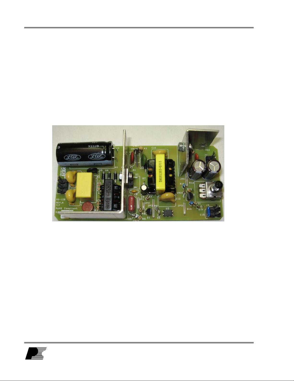
Figure 1 – Populated Circuit Board Photograph.
Page 4 of 32
Power Integrations, Inc.
Tel: +1 408 414 9200 Fax: +1 408 414 9201
www.powerint.com
Page 5
16-Aug-07 RDR-128 36 W, 72 W Peak Variable Output Power Supply
2 Power Supply Specification
Description Symbol Min Typ Max Units Comment
Input
Voltage
Frequency
No-load Input Power (230 VAC) 0.3 W
Output
Output Voltage 1
Output Ripple Voltage 1
Continuous Output Current 1
Peak Output Current 1
Total Output Power
Continuous Output Power
Peak Output Power
Efficiency
Full Load
Environmental
Conducted EMI
Safety
Surge 2 kV
Ambient Temperature
V
f
LINE
IN
90 265 VAC
47 50/60 64 Hz
2 Wire – no P.E.
11.5 12 12.5 V
V
OUT1
V
RIPPLE1
I
OUT1
I
OUTPK
P
OUT
P
OUT_PEAK
800 mV
3 A
6.0 A
36 W
72 W
20 MHz bandwidth
η
80 %
Measured at P
Meets CISPR22B / EN55022B
T
AMB
Designed to meet IEC950, UL1950
0 40
Class II
1.2/50 µs surge, IEC 1000-4-5,
Series Impedance:
Differential Mode: 2 Ω
o
C
Common Mode: 12 Ω
Free convection, sea level
± 5%
OUT
25
o
C
Page 5 of 32
Tel: +1 408 414 9200 Fax: +1 408 414 9201
Power Integrations
www.powerint.com
Page 6
RDR-128 36 W, 72 W Peak Variable Output Power Supply 16-Aug-07
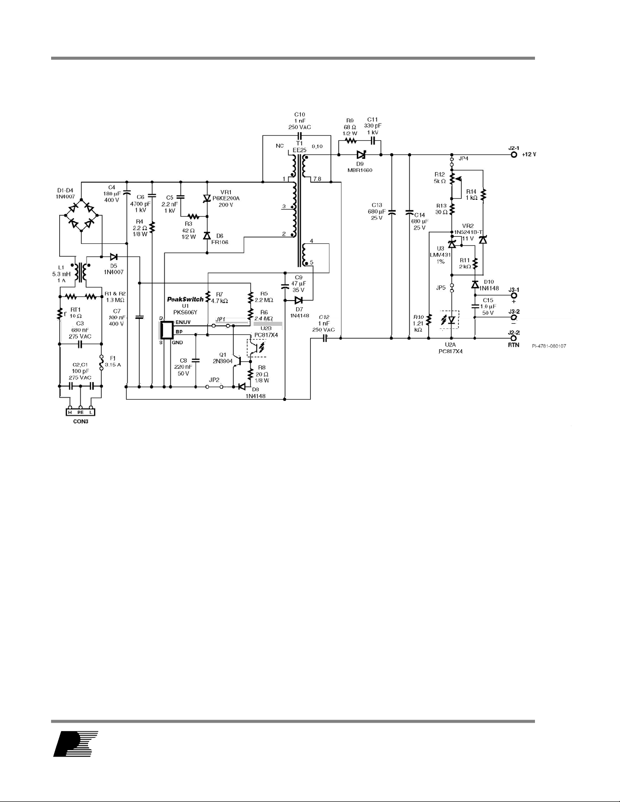
3 Schematic
Figure 2 – Schematic.
Page 6 of 32
Power Integrations, Inc.
Tel: +1 408 414 9200 Fax: +1 408 414 9201
www.powerint.com
Page 7

16-Aug-07 RDR-128 36 W, 72 W Peak Variable Output Power Supply
4 Circuit Description
The motor drive power supply shown in Figure 1 is a switch mode power supply design
utilizing the flyback topology.
4.1 Input EMI Filtering
Differential mode EMI filtering is provided by X-capacitor C3. Y-capacitors C1, C2, C10
and C12, together with the common-mode choke L1, provide common-mode EMI
filtering. Additionally the transformer E-Shields™, together with the frequency jittering
features, provide adequate EMI margins.
4.2 PeakSwitch Primary
Fuse F1 protects the power supply from a catastrophic failure due to a short circuit fault.
A high voltage DC bus is created from the AC line voltage by the full-wave rectifier
formed by diodes D1-D4. Capacitor C4 smoothes and filters the rectified AC voltage.
The PKS606YN (U1) integrates a high voltage MOSFET, along with startup and all
necessary control circuitry.
During the MOSFET’s on-time, current flows through the primary of transformer T1,
storing energy in the transformer core.
During the turn off event, the voltage across the primary winding reverses. A voltage
equal to the sum of DC bus voltage and the reflected output voltage (VOR) appears
across the DRAIN and SOURCE of the PeakSwitch, with an additional spike generated
by the leakage inductance. A primary clamp circuit formed by D6, VR1, R3 and C5 limits
this voltage and resets the leakage energy prior to the next switching cycle.
Diode D7 rectifies the supply’s bias winding while capacitor C9 provides DC filtering.
This bias supply is connected to the PeakSwitch’s BP pin via R7, which powers the
device during normal operation.
4.3 Under-voltage Protection and Fast AC Reset circuit
Under-voltage shutdown is implemented by a separate line rectifying diode, D5, which
charges capacitor C7. Resistors R5 and R6 program the UV start-up voltage to
approximately 104 VDC, which is the DC voltage across C7, at which a current equal to
25 µA flows into the EN/UV pin.
This separate AC line sense network (formed by D5, C7) allows the PeakSwitch to
identify the cause of a fault condition. If the input voltage is above the under-voltage
threshold and the EN/UV pin has not been pulled low for 30 ms, a fault condition is
assumed, and the PeakSwitch latches off. Once the supply is latched off, the AC line
voltage must be removed to allow capacitor C7 to discharge and allow the current into
the EN/UV pin to fall below 25 µA.
Page 7 of 32
Tel: +1 408 414 9200 Fax: +1 408 414 9201
Power Integrations
www.powerint.com
Page 8

RDR-128 36 W, 72 W Peak Variable Output Power Supply 16-Aug-07
If the EN/UV pin has not been pulled low for 30 ms and the input voltage is below the
under-voltage threshold, then the loss of regulation is assumed to be due to a low line
condition, and the PeakSwitch will stop switching until the under-voltage threshold is
exceeded again.
4.4 Output Rectification and Filtering
Diode D9 rectifies the output voltage while capacitors C13 and C14 provide output
filtering. The output capacitor current ripple rating is chosen t6 79S327.74 Bicsin
in52.(mume radedm)]TJ/T64 1 Tf7183 0 TD0.0001 Tc0 Tw(coatiuous/avertag )Tj/TT2 1 Tf58.32 0 TD-0.0005 Tc000077 Tw[a ladg. Resi str R93 andct
Page 8 of 32
Power Integrations, Inc.
Tel: +1 408 414 9200 Fax: +1 408 414 9201
www.powerint.com
Page 9

16-Aug-07 RDR-128 36 W, 72 W Peak Variable Output Power Supply
5 PCB Layout
Figure 3 – Printed Circuit Layout.
Page 9 of 32
Tel: +1 408 414 9200 Fax: +1 408 414 9201
Power Integrations
www.powerint.com
Page 10

RDR-128 36 W, 72 W Peak Variable Output Power Supply 16-Aug-07
6 Bill of Materials
Item Qty Ref Description Mfg Mfg Part
Number
1 2 C1 C2 100 pF, Ceramic, Y1 Panasonic ECK-
ANA101MB
2 1 C3 680 nF, 275 VAC, Film,MPX
Series, X2
3 1 C4 180 uF, 400 V, Electrolytic, Low
ESR, (18 x 40)
4 1 C5 2.2 nF, 1 kV, Disc Ceramic NIC Components
Carli PX684K3ID6
Nippon Chemi-Con EPAG401ELL18
1MM40S
NCD222K1KVY
Corp
5FF
5 1 C6 4700pF, 1 kV, Thru Hole, Disc
Ceramic
6 1 C7 100 nF, 400 V, Film Panasonic ECQ-E4104KF
7 1 C8 220 nF, 50 V, Ceramic, Z5U, 0.2"
L.S.
8 1 C9 47 uF, 35 V, Electrolytic, Gen.
Purpose, (5 x 11)
9 2 C10 C12 1 nF, Ceramic, Y1 Panasonic ECK-
10 1 C11 330 pF, 1 kV, Disc Ceramic Vishay 562R5GAT33
11 2 C13 C14 680 uF, 25 V, Electrolytic, Very
Low ESR, 23 mOhm, (10 x 20)
12 1 C15 1.0 uF, 50 V, Ceramic, X7R Epcos B37984M5105K
13 5 D1 D2 D3
D4 D5
14 1 D6 800 V, 1 A, Fast Recovery Diode,
15 3 D7 D8 D10 75 V, 300 mA, Fast Switching,
16 1 D9 60 V, 10 A, Schottky, TO-220AC Vishay MBR1060
17 1 F1 3.15 A, 250V, Slow, TR5 Wickman 3721315041
18 1 HS PAD1 HEATSINK PAD, TO-220, Sil-Pad
19 1 HS1 HEATSINK/Alum, TO220 1 hole,
20 1 HS2 HEATSINK/Alum, TO220 1 hole,
21 1 J1 3 Position (1 x 3) header, 0.156
22 2 J2 J3 2 Position (1 x 2) header, 0.156
23 2 JP1 JP5 Wire Jumper, Non insulated, 22
24 1 JP2 Wire Jumper, Non insulated, 22
25 2 JP3 JP4 Wire Jumper, Non insulated, 22
1000 V, 1 A, Rectifier, DO-41 Vishay 1N4007
500 ns, DO-41
DO-35
1000
2 mtg pins
2 mtg pins
pitch, Vertical
pitch, Vertical
AWG, 0.4 in
AWG, 0.3 in
AWG, 0.6 in
Vishay/Sprague 562R5GAD47
Kemet C322C224M5U5
CA
Panasonic ECA-1VHG470
ANA102MB
Nippon Chemi-Con EKZE250ELL68
1MJ20S
000
Diodes Inc. FR106
Vishay 1N4148
Bergpuist 1009-58
Clark Precision
Sheetmetal
Clark Precision
Sheetmetal
Molex 26-48-1031
Molex 26-48-1021
Alpha 298
Alpha 298
Alpha 298
60-00012-00
60-00020-00
Page 10 of 32
Power Integrations, Inc.
Tel: +1 408 414 9200 Fax: +1 408 414 9201
www.powerint.com
Page 11

16-Aug-07 RDR-128 36 W, 72 W Peak Variable Output Power Supply
26 1 L1 5.3 mH, 1 A, Common Mode
Choke
27 2 NUT1
NUT2
28 1 Q1 NPN, Small Signal BJT, 40 V, 0.2
29 2 R1 R2 1.3 M, 5%, 1/4 W, Carbon Film Yageo CFR-25JB-1M3
30 1 R3 62 R, 5%, 1/2 W, Carbon Film Yageo CFR-50JB-62R
31 1 R4 2.2 R, 5%, 1/8 W, Carbon Film Yageo CFR-12JB-2R2
32 1 R5 2.2 M, 5%, 1/4 W, Carbon Film Yageo CFR-25JB-2M2
33 1 R6 2.4 M, 5%, 1/4 W, Carbon Film Yageo CFR-25JB-2M4
34 1 R7 4.7 k, 5%, 1/4 W, Carbon Film Yageo CFR-25JB-4K7
35 1 R8 20 R, 5%, 1/8 W, Carbon Film Yageo CFR-12JB-20R
36 1 R9 68 R, 5%, 1/2 W, Carbon Film Yageo CFR-50JB-68R
37 1 R10 1.21 k, 1%, 1/4 W, Metal Film Yageo MFR-25FBF-
38 1 R11 2 k, 5%, 1/4 W, Carbon Film Yageo CFR-25JB-2K0
39 1 R12 5 k,Pot, 20%, 1/8 W, Vertical CTS Corp. 296UD502B1N
40 1 R13 30 R, 5%, 1/4 W, Carbon Film Yageo CFR-25JB-30R
Nut, Hex, Kep 4-40, S ZN Cr3
plateing RoHS
A, TO-92
Panasonic ELF15N010A
On Semiconductor 2N3904RLRAG
1K21
41 1 R14 1 k, 1%, 1/4 W, Metal Film Yageo MFR-25FBF-
1K00
42 1 RT1 NTC Thermistor, 0.34 Ohms, 1.7 A Thermometrics CL-120
43 2 SCREW1
SCREW2
44 1 T1 Transformer, 10 Pins, Vertical Yih-Hwa Enterprises
45 1 U1 PeakSwitch, PKS606YN, TO-22046 1 U2 Opto coupler, 35 V, CTR 30047 1 U3 1.24V Shunt Reg IC National
48 1 VR1 200 V, 600 W, 5%, TVS,
49 1 VR2 11 V, 500 mW, 5%, DO-35 Diodes Inc 1N5241B-T
50 2 WASHER1
WASHER2
51 1 WASHER3 Washer Nylon Shoulder #4 Keystone 3049
SCREW MACHINE PHIL 440X5/16 SS
7C
600%, 4-DIP
DO204AC (DO-15)
WASHER FLAT #4 SS Building Fasteners FWSS 004
Building Fasteners PMSSS 440
0031 PH
YW-360-02B
Santronics
Power Integrations PKS606YN
Sharp PC817XJ0000F
Semiconductor
OnSemi P6KE200ARLG
SNX R1365
LMV431ACZ
Note – Parts listed above are all RoHS compliant
Page 11 of 32
Tel: +1 408 414 9200 Fax: +1 408 414 9201
Power Integrations
www.powerint.com
Page 12

RDR-128 36 W, 72 W Peak Variable Output Power Supply 16-Aug-07
7 Transformer Specification
7.1 Electrical Diagram
1st – ½ Primary
19T X 2 - #31AWG
(filled)
nd
– ½ Primary
2
19T X 2 - #31AWG
(filled)
Shield
7T X 4 - #29AWG
(filled)
Bias
5T X 2 - #29AWG
(Spread)
(scatterd)
2
3
1
NC
4
5
9,10
Secondary
4T X4 - #23AWG_TIW
(in 1.5 layers)
7,8
Figure 4 – Transformer Electrical Diagram.
7.2 Electrical Specifications
Electrical Strength
Primary Inductance
Resonant Frequency
Primary Leakage Inductance
1 second, 60 Hz, from Pins 1-5 to Pins 7 and 10 3000 VAC
Pins 1-2, all other windings open, measured at
100 kHz, 0.4 VRMS
148 µH, ± 12%
Pins 1-2, all other windings open 3 MHz (Min)
4 MHz (Max)
Pins 3-4, with Pins 8-9 shorted, measured at
100 kHz, 0.4 VRMS
6 µH (Max.)
7.3 Materials
Item Description
[1]
[2]
[3]
[4]
[5]
[6]
[7]
Core: PC40EE25-Z, TDK or equivalent gapped for AL of 104 nH/T
Bobbin: EE25 Vertical 10 pin
Magnet Wire: #31 AWG
Magnet Wire: #29 AWG
Triple Insulated Wire: #23 AWG
Tape, 3M 1298 Polyester Film, 2.0 mil thick, 10.7 mm wide
Varnish
2
. Gap approx. 0.47 mm.
Page 12 of 32
Power Integrations, Inc.
Tel: +1 408 414 9200 Fax: +1 408 414 9201
www.powerint.com
Page 13

16-Aug-07 RDR-128 36 W, 72 W Peak Variable Output Power Supply
7.4 Transformer Build Diagram
1
3
1/2 Primary:
19T X 2 - #31AWG
(filled)
7,8
9,10
1
4
5
3
2
Shield:
Secondary:
Bias:
1/2 Primary:
7T X 4 - #29AWG
(filled)
4T X4 - #23AWG_TIW
(in 1.5 layers)
5T X 2 - #29AWG
(Spread)
(scatterd)
19T X 2 - #31AWG
(filled)
Bobbin: EE25 Vertical
Lp = 148 uH
Figure 5 – Transformer Build Diagram.
Page 13 of 32
Tel: +1 408 414 9200 Fax: +1 408 414 9201
Power Integrations
www.powerint.com
Page 14

RDR-128 36 W, 72 W Peak Variable Output Power Supply 16-Aug-07
7.5 Transformer Construction
Bobbin Preparation
1st Half Primary
Winding
Insulation
Bias Winding
Insulation
Secondary Winding
Insulation
Shield Winding
2nd Half Primary
Winding
Insulation
Core Assembly
Varnish
Pin side of the bobbin is oriented to the left hand side. Winding direction is
clockwise when viewed from the non-pin side.
Start on pin 2, wind 19 bi-filar turns of item [3], Magnet Wire: #31 AWG, from left to
right with tight tension and bring the wire back across the bobbin and terminate the
winding on pin 3.
Apply 1 layer of item [6], 3M 1298 Polyester Film tape, for insulation.
Start on pin 5, wind 5 bi-filar turns of item [4], Magnet Wire: #29 AWG, from left to
right, spreading the windings evenly across the bobbin. Bring the wire back across
the bobbin and terminate the winding on pin 4.
Apply 2 layers of item [6], 3M 1298 Polyester Film tape, for insulation.
Start on pin 9 and 10 using 2 wires for each pin. Wind 4 quad-filar turns of item [5],
#23 AWG Triple Insulated Wire, from right to left. Continue winding the second
layer from right to left, spreading the turns evenly across the bobbin. Terminate the
winding on pins 7 and 8 using two wires for each pin.
Apply 2 layers of item [6], 3M 1298 Polyester Film tape, for insulation.
Start on pin 1 and wind 7 quad-filar turns of item [4], Magnet Wire: #29 AWG from
left to right with tight tension across the bobbin. Cut and finish the end.
Start on pin 3, wind 19 bi-filar turns of item [3], Magnet Wire: #31 AWG, from left to
right with tight tension and bring the wire back across the bobbin and terminate the
winding on pin 1.
Apply 3 layers of item [6], 3M 1298 Polyester Film tape, for insulation
Assemble and secure core halves.
Dip varnish assembled transformer with item [7], varnish.
Page 14 of 32
Power Integrations, Inc.
Tel: +1 408 414 9200 Fax: +1 408 414 9201
www.powerint.com
Page 15

16-Aug-07 RDR-128 36 W, 72 W Peak Variable Output Power Supply
8 Transformer Spreadsheet
ACDC_PeakSwitch_020107;
Rev.1.13; Copyright Power
Integrations 2007
ENTER APPLICATION VARIABLES Customer
VACMIN 90 Volts Minimum AC Input Voltage
VACMAX 265 Volts Maximum AC Input Voltage
fL 50 Hertz AC Mains Frequency
Nominal Output Voltage (VO) 12.00
Maximum Output Current (IO) 6.00 Amps Power Supply Output Current (corresponding to peak
Minimum Output Voltage at Peak Load 12.00 Volts Minimum Output Voltage at Peak Power (Assuming
Continuous Power 35.00
Peak Power
n 0.68 Efficiency Estimate at output terminals and at peak
Z 0.60 Loss Allocation Factor (Z = Secondary side losses /
tC Estimate 3.00 mSec
CIN 180.00 180 uFar
ENTER PeakSwitch VARIABLES
PeakSwitch PKS606Y PKS606Y
Chosen Device
ILIMITMIN 2.600 Amps Minimum Current Limit
ILIMITMAX 3.000 Amps Maximum Current Limit
fSmin 250000 Hertz Minimum Device Switching Frequency
I^2fmin 1955 A^2k
VOR 120.00 120 Volts Reflected Output Voltage (VOR <= 135 V
VDS 10 Volts PeakSwitch on-state Drain to Source Voltage
VD 0.7 Volts Output Winding Diode Forward Voltage Drop
VDB 0.7 Volts Bias Winding Diode Forward Voltage Drop
VCLO
KP (STEADY STATE) 0.47 Ripple to Peak Current Ratio (KP < 6)
KP (TRANSIENT) 0.29 Ripple to Peak Current Ratio under worst case at
ENTER UVLO VARIABLES
V_UV_TARGET 96 Volts Target DC under-voltage threshold, above which the
V_UV_ACTUAL 100 Volts Typical DC start-up voltage based on standard value
RUV_IDEAL 3.75 Moh
RUV_ACTUAL 3.90 Moh
BIAS WINDING VARIABLES
VB 15.00 Volts Bias winding Voltage
NB 5 Number of Bias Winding Turns
PIVB 65 Volts Bias rectifier Maximum Peak Inverse Voltage
ENTER TRANSFORMER CORE/CONSTRUCTION VARIABLES
Core Type EE25 EE25 User Selected Core Size(Verify acceptable thermal
Core
Bobbin
INPUT INFO OUTPUT UNIT ACDC_PeakSwitch_020107_Rev1-13.xls;
PKS6
06Y
EE25
EE25_BOBBIN P/N:
Volts Nominal Output Voltage (at continuous power)
35.00 Watts Continuous Output Power
72.00 Watts Peak Output Power
onds
200 Volts Nominal Clamp Voltage
PeakSwitch Continuous/Discontinuous Flyback
Transformer Design Spreadsheet
power)
output droop during peak load)
load. Enter 0.7 if no better data available
Total losses)
Bridge Rectifier Conduction Time Estimate
Input Capacitance
ads
PeakSwitch device
I^2f (product of current limit squared and frequency is
Hz
trimmed for tighter tolerance)
Recommended)
peak load (0.25 < KP < 6)
power supply with start
of RUV_ACTUAL
Calculated value for UV Lockout resistor
ms
Closest standard value of resistor to RUV_IDEAL
ms
rise under continuous load conditions)
P/N:
PC40EE25-Z
EE25_BOBBIN
Page 15 of 32
Tel: +1 408 414 9200 Fax: +1 408 414 9201
Power Integrations
www.powerint.com
Page 16

RDR-128 36 W, 72 W Peak Variable Output Power Supply 16-Aug-07
AE 0.404 cm^2 Core Effective Cross Sectional Area
LE 7.34 cm Core Effective Path Length
AL 1420 nH/T^2 Ungapped Core Effective Inductance
BW 10.20 mm Bobbin Physical Winding Width
M 0.00 mm Safety Margin Width (Half the Primary to
L 2.00
NS 4 4 Number of Secondary Turns
DC INPUT VOLTAGE PARAMETERS
VMIN
VMAX 375 Volts Maximum DC Input Voltage
CURRENT WAVEFORM SHAPE PARAMETERS
DMAX 0.61 Duty Ratio at full load, minimum primary
IAVG 1.37 Amps Average Primary Current
IP 2.60 Amps Minimum Peak Primary Current
IR 1.21 Amps Primary Ripple Current
IRMS 1.82 Amps Primary RMS Current
TRANSFORMER PRIMARY DESIGN PARAMETERS
LP 148 uHenries Typical Primary Inductance. +/- 12% to ensure a
LP_TOLERANCE 12 % Primary inductance tolerance
NP 38 Primary Winding Number of Turns
ALG 104 nH/T^2 Gapped Core Effective Inductance
Target BM
BM 2910 Gauss Calculated Maximum Operating Flux Density, BM <
BAC 677 Gauss AC Flux Density for Core Loss Curves (0.5 X Peak
ur 2053 Relative Permeability of Ungapped Core
LG
BWE 20.4 mm Effective Bobbin Width
OD 0.54 mm Maximum Primary Wire Diameter including
INS 0.07 mm Estimated Total Insulation Thickness (= 2 * film
DIA 0.47 mm Bare conductor diameter
AWG 25 AWG Primary Wire Gauge (Rounded to next smaller
CM 323 Cmils Bare conductor effective area in circular mils
CMA
TRANSFORMER SECONDARY DESIGN PARAMETERS
Lumped parameters
ISP 24.57 Amps Peak Secondary Current
ISRMS 13.82 Amps Secondary RMS Current
IRIPPLE 12.45 Amps Output Capacitor RMS Ripple Current
CMS 2763 Cmils Secondary Bare Conductor minimum circular mils
AWGS 15 AWG Secondary Wire Gauge (Rounded up to next larger
VOLTAGE STRESS PARAMETERS
VDRAIN 665 Volts Maximum Drain Voltage Estimate (Assumes 20%
PIVS 52 Volts Output Rectifier Maximum Peak Inverse Voltage
2 Number of Primary Layers
87 Volts Minimum DC Input Voltage
3000 Gauss Target Peak Flux Density at Maximum Current
0.45 mm Gap Length (Lg > 0.1 mm)
177 Cmils/A
mp
Secondary Creepage Distance)
inductance and minimum input voltage
minimum primary inductance of 132 uH
Limit
3000 is recommended
to Peak)
insulation
thickness)
standard AWG value)
Primary Winding Current Capacity (100 < CMA <
500)
standard AWG value)
zener clamp tolerance and an additional 10%
temperature tolerance)
Page 16 of 32
Power Integrations, Inc.
Tel: +1 408 414 9200 Fax: +1 408 414 9201
www.powerint.com
Page 17

16-Aug-07 RDR-128 36 W, 72 W Peak Variable Output Power Supply
9 Performance Data
The measurements were made at room temperature using open frame convectional
cooling and a line frequency of 60 Hz.
9.1 Efficiency
The efficiency data were obtained at an output power up to 36 W, with the output voltage
set to 12 V and thus a load current of 3 A.
Percent of
Full Load
25
50
75
100
Efficiency (%)
115
VAC
230
VAC
80.2 80.2
81.2 79.8
81.3 80.7
78.2 80.7
Table 1 – Efficiency Data.
Efficiency
82.0%
81.5%
81.0%
80.5%
80.0%
79.5%
79.0%
Efficiency (%)
78.5%
78.0%
77.5%
77.0%
0.500 1.000 1.500 2.000 2.500 3.000
Load (A)
115 VAC
230 VAC
Page 17 of 32
Figure 6 – Efficiency vs. Load, Room Temperature, 60 Hz.
Power Integrations
Tel: +1 408 414 9200 Fax: +1 408 414 9201
www.powerint.com
Page 18

RDR-128 36 W, 72 W Peak Variable Output Power Supply 16-Aug-07
Efficiency vs. Output Voltage at 36 W
84.0%
82.0%
80.0%
78.0%
76.0%
Efficiency
74.0%
72.0%
70.0%
567891011
Output Voltage (V)
115 VAC
230 VAC
Figure 7 – Efficiency vs. Output Voltage with Full Load.
Page 18 of 32
Power Integrations, Inc.
Tel: +1 408 414 9200 Fax: +1 408 414 9201
www.powerint.com
Page 19

16-Aug-07 RDR-128 36 W, 72 W Peak Variable Output Power Supply
9.2 No-load Input Power
No-load Input Power
0.4
0.35
0.3
0.25
0.2
0.15
Input Power (W)
0.1
0.05
0
85 105125145165185205225245265285
Line Voltage (VAC)
Figure 8 – Zero Load Input Power vs. Input Line Voltage, Room Temperature, 60 Hz.
9.3 Regulation
9.3.1 Load
Output Voltage (V)
Load Regulation
12.5
12.45
12.4
12.35
12.3
12.25
12.2
12.15
12.1
12.05
12
0.000 0.500 1.000 1.500 2.000 2.500 3.000
Load (A)
Figure 9 – Load Regulation, Room Temperature.
115 VAC
230 VAC
Page 19 of 32
Tel: +1 408 414 9200 Fax: +1 408 414 9201
Power Integrations
www.powerint.com
Page 20

RDR-128 36 W, 72 W Peak Variable Output Power Supply 16-Aug-07
9.3.2 Line
Line Regulation
12.5
12.45
12.4
12.35
12.3
12.25
12.2
12.15
Output Voltage (V)
12.1
12.05
12
85 135 185 235 285
Line Voltage (VAC)
Figure 10 – Line Regulation, Room Temperature, Full Load.
9.4 Adjustable Output Voltage Characteristics
9.4.1 Resistor Control
Resistor Control Characteristic
14
12
10
8
6
Output Voltage (V)
4
2
012345
Potentiometer, R12 Resistance (kΩ)
Figure 11 – Output Voltage vs. Potentiometer Resistance.
Page 20 of 32
Power Integrations, Inc.
Tel: +1 408 414 9200 Fax: +1 408 414 9201
www.powerint.com
Page 21

16-Aug-07 RDR-128 36 W, 72 W Peak Variable Output Power Supply
9.4.2 External Voltage Control
Control Voltage vs. Output Voltage
14.00
12.00
10.00
8.00
6.00
Output Voltage (V)
4.00
2.00
3.00 3.50 4.00 4.50 5.00 5.50 6.00 6.50 7.00 7.50
Control Voltage (V)
Figure 12 – Output Voltage vs. External Control Voltage.
9.5 Thermal Performance
Thermal testing of the unit was conducted in a thermal chamber under convectional
cooling. The unit was placed horizontally. The volume of convectional cooling was
limited by a cardboard box with dimensions 12” x 10” x 9” (Height x Width x Depth). This
box was used to prevent forced air-cooling of the unit by the thermal chamber’s fan. The
temperature of the PeakSwitch was measured by attaching a thermocouple to the
device’s tab. The output diode’s temperature was monitored in an identical manner. The
unit’s output voltage was approximately 12.5 V during testing with a load of 3 A.
Item
Ambient
PeakSwitch, (U1)
Output Diode, (D9)
Transformer (T1)
Clamp (VR1)
Input Bridge (D1 – D4)
Temperature (°C)
90 VAC 230 VAC
40 40
106 100
91 100
93 94
115 113
86 81
Page 21 of 32
Tel: +1 408 414 9200 Fax: +1 408 414 9201
Power Integrations
www.powerint.com
Page 22

RDR-128 36 W, 72 W Peak Variable Output Power Supply 16-Aug-07
90 VAC, 36 W load, 21ºC Ambient
Figure 13 – Infrared Thermograph of Open Frame Operation at Room Temperature.
Page 22 of 32
Power Integrations, Inc.
Tel: +1 408 414 9200 Fax: +1 408 414 9201
www.powerint.com
Page 23

16-Aug-07 RDR-128 36 W, 72 W Peak Variable Output Power Supply
10 Waveforms
10.1 Drain Voltage and Current, Normal Operation
Figure 14 – 90 VAC, V
Upper: V
Lower: I
DRAIN
DRAIN
Figure 16 – 230 VAC, V
Upper: V
Lower: I
DRAIN
DRAIN
= 12 V, Io= 3 A
out
, 100 V
, 1.0 A / div, 5 µs / div.
= 12 V, Io= 3 A
out
, 100 V
, 1.0 A / div, 5 µs / div.
Figure 15 – 90 VAC, V
Upper: V
Lower: I
Figure 17 – 230 VAC, V
Upper: V
Lower: I
= 2.3 V, Io= 3 A
out
, 100 V
DRAIN
, 1.0 A / div, 5 µs / div.
DRAIN
= 2.3 V, Io= 3 A
out
, 100 V
DRAIN
, 1.0 A / div, 5 µs / div.
DRAIN
Page 23 of 32
Tel: +1 408 414 9200 Fax: +1 408 414 9201
Power Integrations
www.powerint.com
Page 24

RDR-128 36 W, 72 W Peak Variable Output Power Supply 16-Aug-07
10.2 Output Voltage and Current Start-up Profile
Figure 18 – Start-up Profile, 90 VAC
Upper Trace: Output Voltage 5 V / div.
Middle Trace: Output Current 1 A /div.
Lower Trace: DC Bus Voltage 50 V /div.
(Time base – 5 ms / div)
Figure 19 – Start-up Profile, 230 VAC
10.3 Drain Voltage and Current Start-up Profile
Figure 20 – 110 VAC Input
Upper: V
Middle: I
Lower: V
, 2 V / div.
out
, 1 A / div.
DRAIN
, 100 V (5 ms / div)
DRAIN
Figure 21 – 265 VAC Input and Maximum Load. Upper:
Upper Trace: Output Voltage 5 V / div.
Middle Trace: Output Current 1 A /div.
Lower Trace: DC Bus Voltage 100 V /div.
(Time base – 5 ms / div)
, 2 V / div.
V
out
Middle: I
Lower: V
, 1 A / div.
DRAIN
, 100 V (5 ms / div)
DRAIN
Page 24 of 32
Power Integrations, Inc.
Tel: +1 408 414 9200 Fax: +1 408 414 9201
www.powerint.com
Page 25

16-Aug-07 RDR-128 36 W, 72 W Peak Variable Output Power Supply
10.4 Transient Response
Figure 22 – 90 VAC Input
Upper: V
Lower: I
, 500 mV / div. (AC coupled)
out
, 2 A / div.
DRAIN
(10 ms / div)
Figure 23 – 265 VAC Input and Maximum Load.
Upper: V
Lower: I
, 500 mV / div. (AC coupled)
out
, 2 A / div.
DRAIN
(10 ms / div)
10.5 Output Voltage and DC Bus Voltage Ripple
For this measurement the supply’s full peak power was pulsed for approximately 50 ms
and the DC bus voltage was measured in addition to the output voltage’s ripple.
Figure 24 – 90 VAC Input, V
Upper Trace: DC Bus Voltage 100 V /
div.
Middle Trace: V
Lower Trace: I
out
50 ms / div.
Page 25 of 32
=11 V
out
Ripple, 1 V / div.
out
=7 A
Figure 25 – 230 VAC Input, V
Upper Trace: DC Bus Voltage 100 V /
div.
Middle Trace: V
Lower Trace: I
50 ms / div.
Tel: +1 408 414 9200 Fax: +1 408 414 9201
=11 V
out
Ripple, 1 V / div.
out
=12 A
out
Power Integrations
www.powerint.com
Page 26

RDR-128 36 W, 72 W Peak Variable Output Power Supply 16-Aug-07
10.6 Latching Shutdown Operation
The waveform shown below illustrates the power supply’s latching shutdown feature. This
feature is invaluable in a motor application due to the short circuit condition that can
occur if the motor were to become jammed.
Figure 26 – Latching Shutdown Operation.
Page 26 of 32
Power Integrations, Inc.
Tel: +1 408 414 9200 Fax: +1 408 414 9201
www.powerint.com
Page 27

16-Aug-07 RDR-128 36 W, 72 W Peak Variable Output Power Supply
10.7 Output Ripple Measurements
10.7.1 Ripple Measurement Technique
For DC output ripple measurements, a modified oscilloscope test probe must be utilized
in order to reduce spurious signals due to pickup. Details of the probe modification are
provided in the figures below.
The 4987BA probe adapter is affixed with two capacitors tied in parallel across the probe
tip. The capacitors include one (1) 0.1 µF/50 V ceramic type and one (1) 1.0 µF/50 V
aluminum electrolytic. The aluminum electrolytic type capacitor is polarized, so proper
polarity across DC outputs must be maintained (see below).
Probe Ground
Probe Tip
Figure 27 – Oscilloscope Probe Prepared for Ripple Measurement. (End Cap and Ground Lead Removed)
Figure 28 – Oscilloscope Probe with Probe Master (www.probemaster.com) 4987A BNC Adapter.
(Modified with wires for ripple measurement and two parallel decoupling capacitors added)
Page 27 of 32
Tel: +1 408 414 9200 Fax: +1 408 414 9201
Power Integrations
www.powerint.com
Page 28

RDR-128 36 W, 72 W Peak Variable Output Power Supply 16-Aug-07
10.7.2 Measurement Results
Figure 29 – 90 VAC Input, V
Upper Trace: V
Lower Trace: V
out
Drain
(5 µs / div)
Figure 31 – 230 VAC Input, V
Upper Trace: V
Lower Trace: V
out
Drain
(5 µs / div)
=12 V, Io = 3 A
out
Ripple, 500 mV / div.
, 100 V /div.
=12 V, Io = 3 A
out
Ripple, 500 mV / div.
, 100 V /div.
Figure 30 – 90 VAC Input, V
Upper Trace: V
Lower Trace: V
(5 µs / div)
Figure 32 – 230 VAC Input, V
Upper Trace: V
Lower Trace: V
(5 µs / div)
=2.3 V, Io = 3 A
out
Ripple, 500 mV / div.
out
, 100 V /div.
Drain
=12 V, Io = 3 A
out
Ripple, 500 mV / div.
out
, 100 V /div.
Drain
Page 28 of 32
Power Integrations, Inc.
Tel: +1 408 414 9200 Fax: +1 408 414 9201
www.powerint.com
Page 29

16-Aug-07 RDR-128 36 W, 72 W Peak Variable Output Power Supply
11 Conducted EMI
The following worst case conducted EMI measurements were made with a load of 3 A
with the output grounded.
Figure 33 – Conducted EMI, Maximum Steady State Load, 90 VAC, 60 Hz, and EN55022 B Limits.
Figure 34 – Conducted EMI, Maximum Steady State Load, 230 VAC, 60 Hz, and EN55022 B Limits.
Page 29 of 32
Tel: +1 408 414 9200 Fax: +1 408 414 9201
Power Integrations
www.powerint.com
Page 30

RDR-128 36 W, 72 W Peak Variable Output Power Supply 16-Aug-07
12 Revision History
Date Author Revision Description & changes Reviewed
16-Aug-07 SK 1.0 Initial Publication
Page 30 of 32
Power Integrations, Inc.
Tel: +1 408 414 9200 Fax: +1 408 414 9201
www.powerint.com
Page 31

16-Aug-07 RDR-128 36 W, 72 W Peak Variable Output Power Supply
Notes
Page 31 of 32
Tel: +1 408 414 9200 Fax: +1 408 414 9201
Power Integrations
www.powerint.com
Page 32

RDR-128 36 W, 72 W Peak Variable Output Power Supply 16-Aug-07
For the latest updates, visit our website: www.powerint.com
Power Integrations reserves the right to make changes to its products at any time to improve reliability or manufacturability. Power
Integrations does not assume any liability arising from the use of any device or circuit described herein. POWER INTEGRATIONS
MAKES NO WARRANTY HEREIN AND SPECIFICALLY DISCLAIMS ALL WARRANTIES INCLUDING, WITHOUT
LIMITATION, THE IMPLIED WARRANTIES OF MERCHANTABILITY, FITNESS FOR A PARTICULAR PURPOSE, AND
NON-INFRINGEMENT OF THIRD PARTY RIGHTS.
PATENT INFORMATION
The products and applications illustrated herein (incl uding transformer construction and circuits external to the products)
may be covered by one or more U.S. and foreign patents, or potentially by pen ding U.S. and foreign patent app lications
assigned to Power Integrations. A complete list of Power Integrations’ patents may be found at www.powerint.com
.
Power Integrations grants its customers a license under certain patent rights as set forth at
http://www.powerint.com/ip.htm.
The PI Logo, TOPSwitch, TinySwitch, LinkSwitch, DPA-Switch, PeakSwitch, EcoSmart, Clampless, E-Shield, Filterfuse, PI Expert and PI FACTS
are trademarks of Power Integrations, Inc. Other trademarks are property of their respective companies. ©Copyright 2006 Power
Integrations, Inc.
Power Integrations Worldwide Sales Support Locations
WORLD HEADQUARTERS
5245 Hellyer Avenue
San Jose, CA 95138, USA.
Main: +1-408-414-9200
Customer Service:
Phone: +1-408-414-9665
Fax: +1-408-414-9765
e-mail: usasales@powerint.com
CHINA (SHANGHAI)
Rm 807-808A,
Pacheer Commercial Centre,
555 Nanjing Rd. West
Shanghai, P.R.C. 200041
Phone: +86-21-6215-5548
Fax: +86-21-6215-2468
chinasales@powerint.com
e-mail:
CHINA (SHENZHEN)
Room 2206-2207, Block A,
Elec. Sci. Tech. Bldg.
2070 Shennan Zhong Rd.
Shenzhen, Guangdong,
China, 518031
Phone: +86-755-8379-3243
Fax: +86-755-8379-5828
e-mail: chinasales@powerint.com
GERMANY
Rueckertstrasse 3
D-80336, Munich
Germany
Phone: +49-89-5527-3910
Fax: +49-89-5527-3920
e-mail: eurosales@powerint.com
INDIA
261/A, Ground Floor
7th Main, 17th
Sadashivanagar
Bangalore, India 560080
Phone: +91-80-5113-8020
Fax: +91-80-5113-8023
e-mail: indiasales@powerint.com
ITALY
Via Vittorio Veneto 12
20091 Bresso MI
Italy
Phone: +39-028-928-6000
Fax: +39-028-928-6009
e-mail: eurosales@powerint.com
Cross,
JAPAN
Keihin Tatemono 1
2-12-20
Shin-Yokohama, Kohoku-ku,
Yokohama-shi, Kanagawa ken,
Japan 222-0033
Phone: +81-45-471-1021
Fax: +81-45-471-3717
e-mail:
japansales@powerint.com
KOREA
RM 602, 6FL
Korea City Air Terminal B/D,
159-6
Samsung-Dong, Kangnam-Gu,
Seoul, 135-728, Korea
Phone: +82-2-2016-6610
Fax: +82-2-2016-6630
e-mail:
koreasales@powerint.com
SINGAPORE
51 Newton Road,
#15-08/10 Goldhill Plaza,
Singapore, 308900
Phone: +65-6358-2160
Fax: +65-6358-2015
e-mail:
singaporesales@powerint.com
st
Bldg
TAIWAN
5F, No. 318, Nei Hu Rd., Sec. 1
Nei Hu Dist.
Taipei, Taiwan 114, R.O.C.
Phone: +886-2-2659-4570
Fax: +886-2-2659-4550
e-mail:
taiwansales@powerint.com
EUROPE HQ
1st Floor, St. James’s House
East Street, Farnham
Surrey, GU9 7TJ
United Kingdom
Phone: +44 (0) 1252-730-140
Fax: +44 (0) 1252-727-689
e-mail: eurosales@powerint.com
APPLICATIONS HOTLINE
World Wide +1-408-414-9660
APPLICATIONS FAX
World Wide +1-408-414-9760
Page 32 of 32
Power Integrations, Inc.
Tel: +1 408 414 9200 Fax: +1 408 414 9201
www.powerint.com
 Loading...