

Page 1
LNK501
®
LinkSwitch
™
Family
Energy Efficient, CV/CC Switcher for
Very Low Cost Chargers and Adapters
Product Highlights
Cost Effective Linear/RCC Replacement
• Lowest cost, component count, constant voltage, constant
current (CV/CC) solution
• Extremely simple circuit configuration
• Up to 75% lighter power supply reduces shipping cost
• Primary based CV/CC solution eliminates 10 to 20
secondary components for low system cost
• Combined primary clamp, feedback, IC supply, and loop
compensation functions–minimizes external components
• Fully integrated auto-restart for short circuit and open
loop fault protection–saves external component costs
• 42 kHz operation simplifies EMI filter design
•3 W output with EE13 core for low cost and small size
Much Higher Performance Over Linear/RCC
• Universal input range allows worldwide operation
• Up to 70% reduction in power dissipation–reduces
enclosure size significantly
• CV/CC output characteristic without secondary feedback
• System level thermal and current limit protection
•Meets all single point failure requirements with only one
additional clamp capacitor
• Controlled current in CC region provides inherent soft-start
• Optional opto feedback improves output voltage accuracy
V
O
*Estimated tolerance achievable in high volume production
including transformer and other component tolerances.
**See Optional Secondary Feedback section.
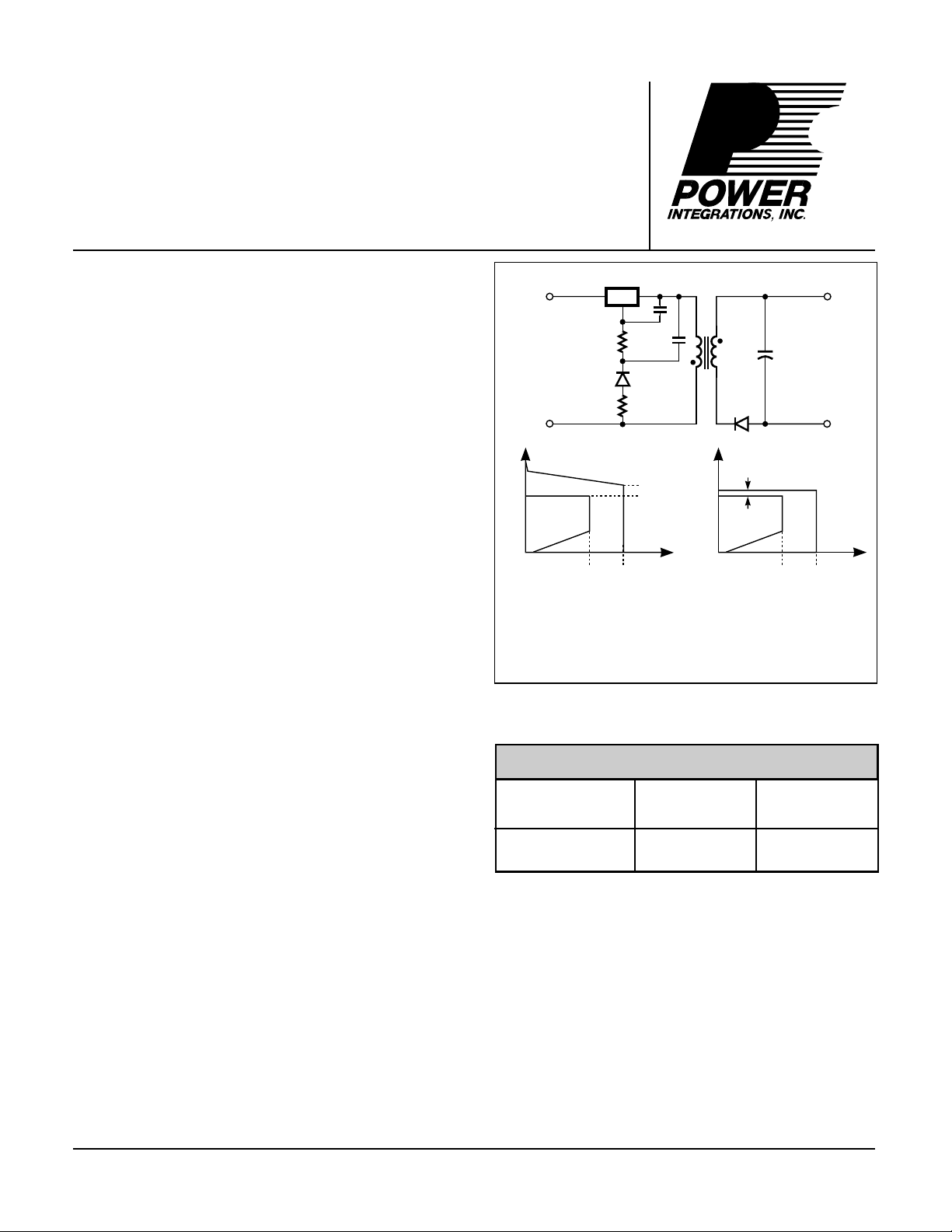
Figure 1. Typical Application – not a Simplified Circuit (a) and
LinkSwitch
DS
C
Wide Range
HV DC Input
(a)
V
O
±5%
±10%
I
±20%*
For Circuit
Shown Above
Output Characteristic Tolerance Envelopes (b).
O
(b)
Secondary Feedback**
Output
±20%*
With Optional
PI-2776-091302
(V
DC
)
O
I
O
EcoSmart
®
- Extremely Energy Efficient
• Consumes <300 mW at 265 VAC input with no load
•Meets Blue Angel, Energy Star, and EC requirements
• No current sense resistors–maximizes efficiency
Applications
• Linear transformer replacement in all ≤ 3 W applications
• Chargers for cell phones, cordless phones, PDAs, digital
cameras, MP3/portable audio devices, shavers, etc.
• Home appliances, white goods and consumer electronics
• TV standby and other auxilliary supplies
Description
LinkSwitch is specifically designed to replace all linear transformer/
RCC chargers and adapters in the ≤ 3 W universal range at equal
or lower system cost with much higher performance and energy
efficiency. LinkSwitch introduces a revolutionary topology for the
design of low power switching power supplies that rivals the
simplicity and low cost of linear adapters, and enables a much
OUTPUT POWER TABLE
PRODUCT
2
230 VAC ±15%
1
85-265 VAC
LNK501 P or G 4 W 3 W
Table 1. Notes: 1. Typical output power for a design achieving
<300 mW no load consumption in an enclosed adapter measured at
50 °C ambient. Higher reflected voltage will extend power capability
with increased no load consumption. See Key Application
Considerations. 2. See Part Ordering Information.
smaller, lighter, and attractive package when compared with the
traditional "brick". With efficiency of up to 75% at 3 W output and
< 300 mW no-load consumption, a LinkSwitch solution can save
the end user enough energy over a linear design to completely
pay for the power supply cost in less than one year. LinkSwitch
integrates a 700 V power MOSFET, PWM control, high voltage
start-up, current limit, and thermal shutdown circuitry, onto a
monolithic IC.
September 2002
Page 2
LNK501
CONTROL
I
DCS
Z
C
SHUNT REGULATOR/
ERROR AMPLIFIER
I
FB
OSCILLATOR
R
E
V
C
D
MAX
CLOCK
SAW
0
INTERNAL
SUPPLY
1
SHUTDOWN/
AUTO-RESTART
+
5.7 V
5.7
4.7
COMPARATOR
+
V
-
V
HYSTERETIC
THERMAL
SHUTDOWN
+
PW
M
LOW
FREQUENCY
OPERATION
÷ 8
SRQ
CURRENT
LIMIT
ADJUST
CURRENT LIMIT
COMPARATOR
+
LEADING
EDGE
EDGE
BLANKING
DRAIN
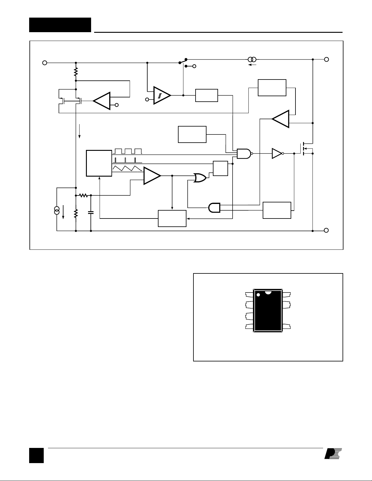
Figure 2. Block Diagram.
Pin Functional Description
DRAIN (D) Pin:
Power MOSFET drain connection. Provides internal operating
current for start-up. Internal current limit sense point for drain
current.
CONTROL (C) Pin:
Error amplifier and feedback current input pin for duty cycle
and current limit control. Internal shunt regulator connection to
provide internal bias current during normal operation. It is also
used as the connection point for the supply bypass and autorestart/compensation capacitor.
SOURCE (S) Pin:
Output MOSFET source connection for high voltage power
return. Primary side control circuit common and reference
point.
S
1
S
2
S
3
S
4
P Package (DIP-8B)
G Package (SMD-8B)
Figure 3. Pin Configuration.
LNK501
SOURCE
PI-2777-071802
C
8
S
7
5
D
PI-2711-073107
F
2
9/02
Page 3
LNK501
S
C
C2
h
LinkSwitch
Functional Description
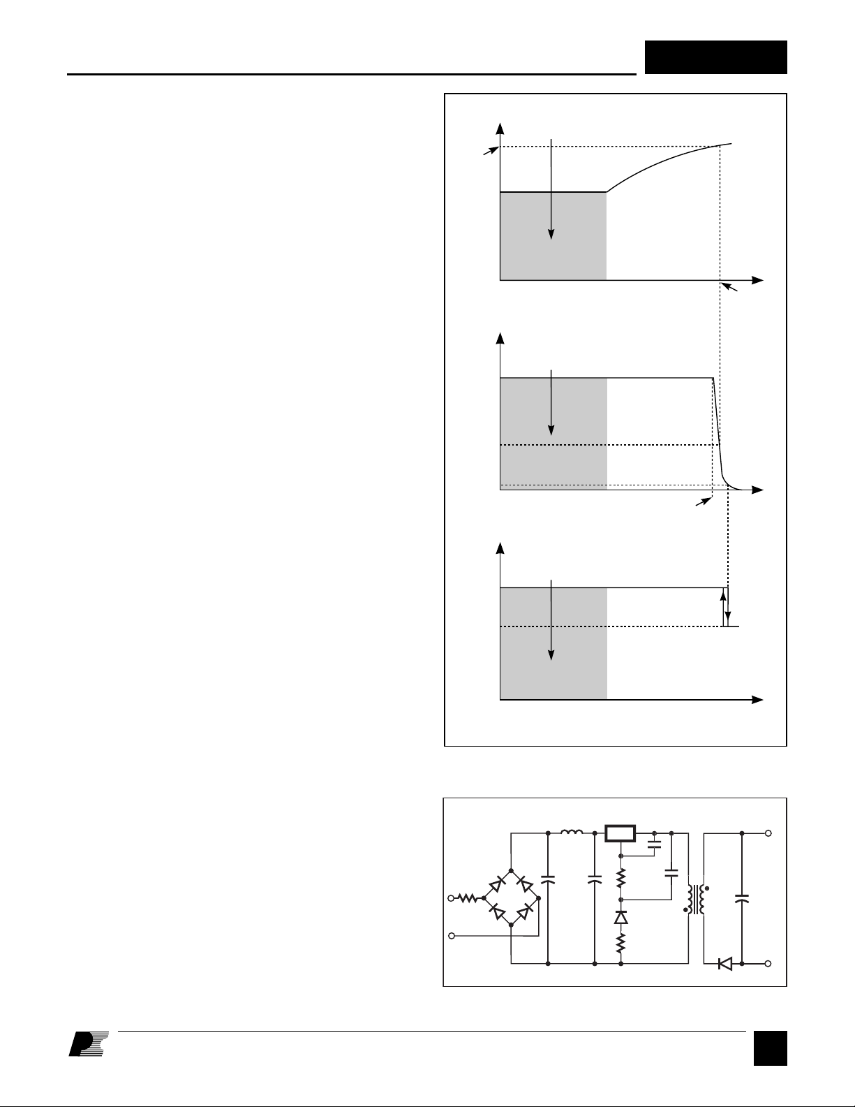
The duty cycle, current limit and operating frequency
relationships with CONTROL pin current are shown in
Figure 4. Figure 5 shows a typical power supply outline
schematic which is used below to describe the LinkSwitch
operation.
Power Up
During power up, as VIN is first applied (Figure 5), the
CONTROL pin capacitor C1 is charged through a switched
high voltage current source connected internally between the
DRAIN and CONTROL pins (see Figure 2). When the
CONTROL pin voltage reaches approximately 5.7 V relative
to the SOURCE pin, the high voltage current source is turned
off, the internal control circuitry is activated and the high
voltage internal MOSFET starts to switch. At this point, the
charge stored on C1 is used to supply the internal consumption
of the chip.
Constant Current (CC) Operation
As the output voltage, and therefore the reflected voltage across
the primary transformer winding ramp up, the feedback
CONTROL current I
internal current limit increases with IC and reaches I
is equal to I
. The internal current limit vs. IC characteristic
DCT
increases. As shown in Figure 4, the
C
LIM
when I
is designed to provide an approximately constant power supply
output current as the power supply output voltage rises.
Constant Voltage (CV) Operation
When IC exceeds I
, typically 2 mA (Figure 4), the maximum
DCS
duty cycle is reduced. At a value of IC that depends on power
supply input voltage, the duty cycle control limits LinkSwitch
peak current below the internal current limit value. At this point
the power supply transitions from CC to CV operation. With
minimum input voltage in a typical universal input design, this
transition occurs at approximately 30% duty cycle. R1
(Figure 5) is therefore initially selected to conduct a value of I
approximately equal to I
when V
DCT
is at the desired value
OUT
at the minimum power supply input voltage. The final choice
of R1 is made when the rest of the circuit design is complete.
When the duty cycle drops below approximately 4%, the
frequency is reduced, which reduces energy consumption
under light load conditions.
Internal Current Limit
Auto-restart
I
LIM
CONTROL Current I
Duty Cycle
Auto-restart
77%
30%
3.8%
C
Frequency
f
OSC
f
OSC(low)
C
CONTROL Current I
Auto-restart
CONTROL Current I
Figure 4. CONTROL Characteristics.
I
CD1
LinkSwitc
D
C
I
DCS
C
C
I
DCT
PI-2799-112101
Auto-Restart Operation
When a fault condition, such as an output short circuit or open
loop, prevents flow of an external current into the CONTROL
pin, the capacitor C1 discharges towards 4.7 V. At 4.7 V, autorestart is activated, which turns the MOSFET off and puts the
control circuitry in a low current standby mode. In auto-restart,
LinkSwitch periodically restarts the power supply so that normal
power supply operation can be restored when the fault is
removed.
V
IN
D1
R2
Figure 5. Power Supply Outline Schematic.
V
C4
D2
OUT
PI-2715-100801
F
9/02
3
Page 4
LNK501
The characteristics described above provide an approximate
CV/CC power supply output without the need for secondary
side voltage or current feedback. The output voltage regulation
is influenced by how well the voltage across C2 tracks the
reflected output voltage. This tracking is influenced by the
value of the transformer leakage inductance which introduces
an error. Resistor R2 and capacitor C2 partially filter the
leakage inductance voltage spike reducing this error. This
circuitry, used with standard transformer construction
techniques provides much better output load regulation than a
linear transformer, making this an ideal power supply solution
in many low power applications. If tighter load regulation is
required, an optocoupler configuration can be used while still
employing the constant output current characteristics provided
by LinkSwitch.
Optional Secondary Feedback
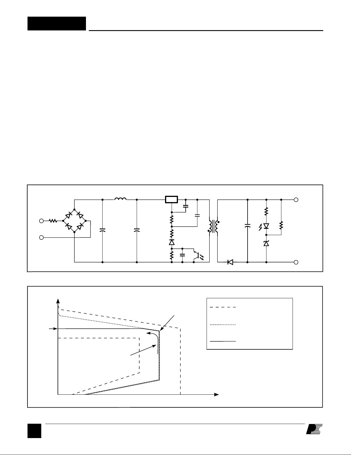
Figure 6 shows a typical power supply outline schematic using
LinkSwitch with optocoupler feedback to improve output voltage
regulation. On the primary side, the schematic differs from
LinkSwitch
LNK501
R1
85-265
VAC
R2
D1
R3
Figure 5 by the addition of R3, C3 and optocoupler U1. R3
forms a potential divider with R1 to limit the U1 collector
emitter voltage.
On the secondary side, the addition of voltage sense circuit
components R4, VR1 and U1 LED provide the voltage feedback
signal. In the example shown, a simple Zener (VR1) reference
is used though more accurate references may be employed for
improved output voltage tolerancing and cable drop
compensation, if required. R4 provides biasing for VR1. The
regulated output voltage is equal to the sum of the VR1 Zener
voltage plus the forward voltage drop of the U1 LED. R5 is an
optional low value resistor to limit U1 LED peak current due to
output ripple. Manufacturer’s specifications for U1 current and
VR1 slope resistance should be consulted to determine whether
R5 is required.
U1 is arranged with collector connected to primary ground and
emitter to the anode of D1. This connection keeps the opto in an
electrically “quiet” position in the circuit. If the opto was
SD
C
C3
C1
C2
R5
U1
R4
VR1
U1
V
OUT
RTN
PI-2787-092002
Figure 6. Power Supply Outline Schematic with Optocoupler Feedback.
Output V oltage
Inherent
CC to CV
transition
Voltage
feedback
threshold
Load variation
during battery
charging
point
Output Current
Figure 7. Influence of the Optocoupler on the Power Supply Output Characteristic.
F
4
9/02
Tolerance envelope
without optocoupler
Typical inherent
characteristic without
optocoupler
Characteristic with
optocoupler
PI-2788-092101
Page 5
LNK501
instead placed on the cathode side of D1, it would become a
switching node, generating additional common mode EMI
currents through its internal parasitic capacitance.
The feedback configuration in Figure 6 is simply a resistive
divider made up of R1 and R3 with D1, R2, C1 and C2 rectifying,
filtering and smoothing the primary winding voltage signal. The
optocoupler therefore effectively adjusts the resistor divider ratio
to control the DC voltage across R1 and therefore, the feedback
current received by the LinkSwitch CONTROL pin.
When the power supply operates in the constant current (CC)
region, for example when charging a battery, the output voltage
is below the voltage feedback threshold defined by U1 and VR1
and the optocoupler is fully off. In this region, the circuit
behaves exactly as previously described with reference to
Figure 5 where the reflected voltage increases with increasing
output voltage and the LinkSwitch internal current limit is
adjusted to provide an approximate CC output characteristic.
Note that for similar output characteristics in the CC region, the
value of R1 in Figure 5 will be equal to the value of R1+R3 in
Figure 6.
When the output reaches the voltage feedback threshold set by
U1 and VR1, the optocoupler turns on. Any further increase in
the power supply output voltage results in the U1 transistor
current increasing, which increases the percentage of the reflected
voltage appearing across R1. The resulting increase in the
LinkSwitch CONTROL current reduces the duty cycle according
to Figure 4 and therefore, maintains the output voltage regulation.
Normally, R1 and R3 are chosen to be equal in value. However,
increasing R3 (while reducing R1 to keep R1 + R3 constant)
increases loop gain in the CV region, improving load regulation.
The extent to which R3 can be increased is limited by opto
transistor voltage and dissipation ratings and should be fully
tested before finalizing a design. The values of C2 and C3 are
less important other than to make sure they are large enough to
have very little influence on the impedance of the voltage
division circuit set up by R1, R3 and U1 at the switching
frequency. Normally, the values of C2 and C3 in Figure 6 are
chosen equal to the value of C2 in Figure 5, though the voltage
rating may be reduced depending on the relative values of R1
and R2 discussed above. See Applications section for typical
values of components.
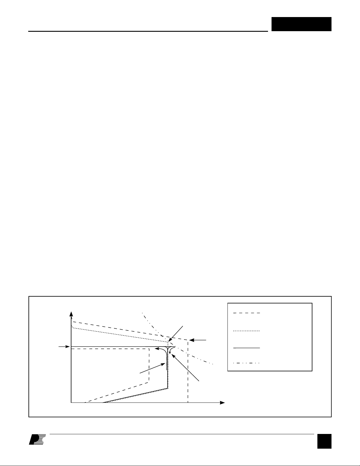
Figure 7 shows the influence of optocoupler feedback on the
output characteristic. The envelope defined by the dashed lines
represent the worst case power supply DC output voltage and
current tolerances (unit-to-unit and over the input voltage
range) if an optocoupler is not used. A typical example of an
inherent (without optocoupler) output characteristic is shown
dotted. This is the characteristic that would result if U1, R4 and
VR1 were removed. The optocoupler feedback results in the
characteristic shown by the solid line. The load variation arrow
in Figure 7 represents the locus of the output characteristic
normally seen during a battery charging cycle. The two
characteristics are identical as the output voltage rises but then
separate as shown when the voltage feedback threshold is
reached. This is the characteristic seen if the voltage feedback
threshold is above the output voltage at the inherent CC to CV
transition point also indicated in Figure 7.
Figure 8 shows a case where the voltage feedback threshold is
set below the voltage at the inherent CC to CV transition point.
In this case, as the output voltage rises, the secondary feedback
circuit takes control before the inherent CC to CV transition
occurs. In an actual battery charging application, this simply
limits the output voltage to a lower value.
Output V oltage
Voltage
feedback
threshold
Load variation
during battery
charging
Figure 8. Output Characteristic with Optocoupler Regulation (Reduced Voltage Feedback Threshold).
Inherent
CC to CV
transition
point
V
O(MAX)
Characteristic observed with
load variation often applied during
laboratory bench testing
Output Current
Tolerance envelope
without optocoupler
Typical inherent
characteristic without
optocoupler
Characteristic with
optocoupler
Power Supply peak
output power curve
PI-2790-092101
9/02
F
5
Page 6

LNK501
However, in laboratory bench tests, it is often more convenient
to test the power supply output characteristic starting from a low
output current and gradually increasing the load. In this case,
the optocoupler feedback regulates the output voltage until the
peak output power curve is reached as shown in Figure 8. Under
these conditions, the output current will continue to rise until
the peak power point is reached and the optocoupler turns off.
Once the optocoupler is off, the CONTROL pin feedback
current is determined only by R1 and R3 and the output current
therefore folds back to the inherent CC characteristic as shown.
Since this type of load transition does not normally occur in a
battery charger, the output current never overshoots the inherent
constant current value in the actual application.
In some applications it may be necessary to avoid any output
current overshoot, independent of the direction of load variation.
To achieve this goal, the minimum voltage feedback threshold
should be set at V
. This will ensure that the voltage at the
O(MAX)
CC to CV transition point of the inherent characteristic will
always occur below the voltage feedback threshold. However,
the output voltage tolerance is then increased, since the inherent
CV characteristic tolerance below V
is added to the
O(MAX)
tolerance of the optocoupler feedback circuit.
Applications Example
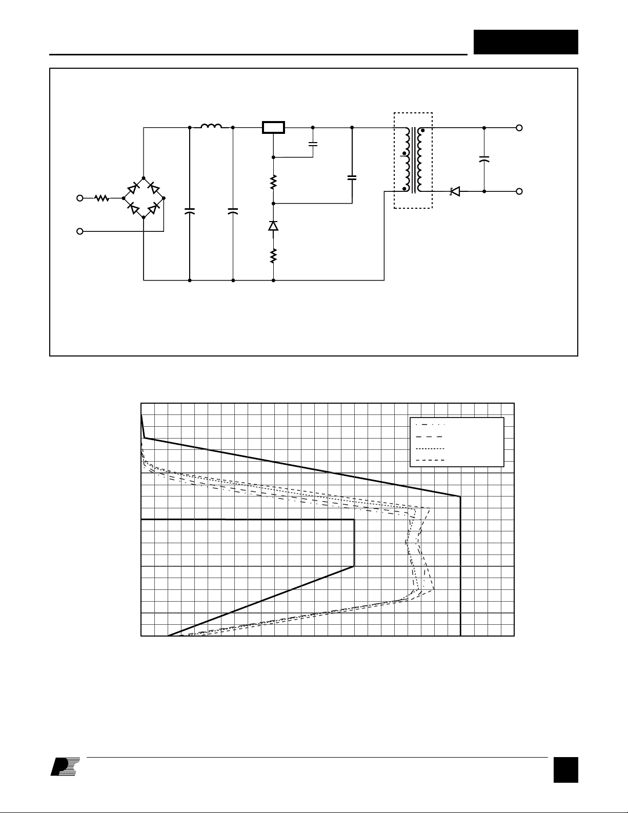
The circuit shown in Figure 9 shows a typical implementation
of an approximate constant voltage / constant current (CV/CC)
charger using LinkSwitch. This design delivers 2.75 W with a
nominal peak power point voltage of 5.5 V and a current of
500 mA. Efficiency is greater than 70% over an input range of
85 VAC to 265 VAC.
The bridge rectifier, BR1, rectifies the AC input. Resistor, RF1
is a fusible type providing protection from primary side short
circuits. The rectified AC is smoothed by C1 and C2 with
inductor L1 forming a pi-filter in conjunction with C1 and C2
to filter conducted EMI. The switching frequency of 42 kHz
allows such a simple EMI filter to be used without the need for
a Y capacitor while still meeting international EMI standards.
When power is applied, high voltage DC appears at the DRAIN
pin of LinkSwitch (U1). The CONTROL pin capacitor C3 is then
charged through a switched high voltage current source connected
internally between the DRAIN and CONTROL pins. When the
CONTROL pin reaches approximately 5.7 V relative to the
SOURCE pin, the internal current source is turned off. The
internal control circuitry is activated and the high voltage MOSFET
starts to switch, using the energy in C3 to power the IC.
When the MOSFET is on, the high voltage DC bus is connected
to one end of the transformer primary, the other end being
connected to primary return. As the current ramps in the
primary of flyback transformer T1, energy is stored. This
energy is delivered to the output when the MOSFET turns off
each switching cycle.
The secondary of the transformer is rectified and filtered by D6
and C5 to provide the DC output to the load.
LinkSwitch dramatically simplifies the secondary side by
controlling both the constant voltage and constant current
regions entirely from the primary side. This is achieved by
monitoring the primary-side VOR (voltage output reflected).
Diode D5 and capacitor C4 form the primary clamp network.
This both limits the peak drain voltage due to leakage inductance
and provides a voltage across C4, which is equal to the VOR plus
an error due to the parasitic leakage inductance. Resistor R2
filters the leakage inductance spike and reduces the error in the
value of the VOR. Resistor R1 converts this voltage into a current
that is fed into the CONTROL pin to regulate the output.
During CV operation the output is regulated through control of
the duty cycle. As the current into the CONTROL pin exceeds
approximately 2 mA, the duty cycle begins to reduce, reaching
30% at a CONTROL pin current of 2.3 mA.
Under light or no-load conditions, when the duty cycle reaches
approximately 4%, the switching frequency is reduced to lower
energy consumption.
If the output load is increased beyond the peak power point
(defined by 0.5·L·I2·f), the output voltage and VOR falls. The
reduced CONTROL pin current will lower the internal
LinkSwitch current limit (current limit control) providing an
approximately constant current output characteristic. If the load
is increased and the CONTROL pin current falls below
approximately 1 mA, the CONTROL pin capacitor C3 will
discharge and the supply enters auto-restart.
Current limit control removes the need for any secondary side
current sensing components (sense resistor, transistor, opto
coupler and associated components). Removing the secondary
sense circuit dramatically improves efficiency, giving the
associated benefit of reduced enclosure size.
Key Application Considerations
Design Output Power
Table 1 (front page) shows the maximum continuous output
power that can be obtained under the following conditions:
1. The minimum DC input bus voltage is 90 V or higher. This
corresponds to a filter capacitor of 3 µF/W for universal
input and 1 µF/W for 230 VAC or 115 VAC input with
doubler input stage.
2. Design is a discontinuous mode flyback converter, with
nominal primary inductance value and a VOR in the range
40-60 V. Note: The simple LinkSwitch circuit configuration
is designed specifically for discontinuous mode operation.
F
6
9/02
Page 7
RF1
10 Ω 1 W
Fusible
85-265
VAC
BR1
1 A, 600 V
L1
1 mH
C1
4.7 µF
400 V
U1
LNK501
LinkSwitch
D
C
C2
4.7 µF
400 V
S
R1
20.5 kΩ
1%
D5
1N4937
R2
100 Ω
C3
0.22 µF
50 V
C4
0.1 µF
100 V
116 T
#34 AWG
LNK501
T1
1
5
4
3
EE13
= 2.55 mH
L
P
15 T
#30 AWG
TIW
6
D6
11DQ06
C5
470 µF
10 V
PERFORMANCE SUMMARY
Output Power: 2.75 W
Efficiency: ≥72%
No Load
Consumption: 260 mW, 230 VAC
200 mW, 115 VAC
5.5 V ,
500 mA
RTN
PI-2904-083002
Figure 9. 2.75 W Constant Voltage/Constant Current (CV/CC) Charger using LinkSwitch.
10
9
8
7
V)
,
OUT
6
5
4
3
Output Voltage (V
2
1
0
1000 200 300 400 500 600 700
Output Current (I
OUT
mA)
,
V
IN
= 85 VAC
V
IN
= 115 VAC
V
IN
= 185 VAC
V
IN
= 265 VAC
PI-2964-072202
Figure 10. Measured Output Characteristic of the Circuit in Figure 9.
9/02
F
7
Page 8

LNK501
Continuous mode designs can result in loop instability and
are therefore not recommended.
3. A secondary output of 5 V with a Schottky rectifier diode.
4. Assumed efficiency of 70%
5. The part is board mounted with SOURCE pins soldered to
sufficient area of copper to keep the die temperature at or
below 100 °C.
In addition to the thermal environment (sealed enclosure,
ventilated, open frame, etc), the maximum power capability of
LinkSwitch in a given application depends on transformer core
size, efficiency, primary inductance tolerance, minimum
specified input voltage, input storage capacitance, output voltage
output diode forward drop etc., and can be different from the
values shown in Table 1.
In designs not required to meet 300 mW no-load consumption,
the transformer can be designed with higher VOR to extend
power capability as noted in the following section.
Transformer Design
To provide an approximately CV/CC output, the transformer
should be designed to be discontinuous; all the energy stored in
the transformer is transferred to the secondary during the
MOSFET off time. Energy transfer in discontinuous mode is
independent of line voltage.
The peak power point prior to entering constant current operation
is defined by the maximum power transferred by the transformer.
The power transferred is given by the expression P = 0.5·L·I2·f,
where L is the primary inductance, I2 is the primary peak current
squared and f is the switching frequency.
To simplify analysis, the data sheet parameter table specifies an
I2f coefficient. This is the product of current limit squared and
switching frequency normalized to the feedback parameter
I
. This provides a single term that specifies the variation of
DCT
the peak power point in the power supply due to LinkSwitch.
As primary inductance tolerance is part of the expression that
determines the peak output power point (start of the CC
characteristic) this parameter should be well controlled. For an
estimated overall output peak power tolerance of ±20% the
primary inductance tolerance should be ±10% or better. This is
achievable using standard low cost, center leg gapping techniques
where the gap size is typically 0.08 mm or larger. Smaller gap
sizes are possible but require non standard, tighter ferrite A
tolerances.
Other gapping techniques such as film gapping allow tighter
tolerances (±7% or better) with associated improvements in the
tolerance of the peak power point. Please consult your
transformer vendor for guidance.
Core gaps should be uniform. Uneven core gapping, especially
with small gap sizes, may cause variation in the primary
inductance with flux density (partial saturation) and make the
constant current region non-linear. To verify uniform gapping
it is recommended that the primary current wave-shape be
examined while feeding the supply from a DC source. The
gradient is defined as di/dt = V/L and should remain constant
throughout the MOSFET on time. Any change in gradient of
the current ramp is an indication of uneven gapping.
Measurements made using a LCR bridge should not be solely
relied upon; typically these instruments only measure at currents
of a few milliamps. This is insufficient to generate high enough
flux densities in the core to show uneven gapping.
For a typical EE13 core using center leg gapping, a 0.08 mm gap
(ALG of 190 nH/t2) allows a primary inductance tolerance of
±10% to be maintained in standard high volume production.
This allows the EE13 to be used in designs up to 2.75 W. If film
gapping is used then this increases to 3 W with less than
300 mW no-load consumption. Moving to a larger core, EE16
for example, allows a 3 W output with center leg gapping.
The transformer turns ratio should be selected to give a V
(output voltage reflected through secondary to primary turns
ratio) of 40 - 60 V. In designs not required to meet 300 mW noload consumption targets, the transformer can be designed with
higher VOR as long as discontinuous mode operation is
maintained. This increases the output power capability. For
example, a 230 VAC input design using an EE19 transformer
core with VOR >70 V, is capable of delivering up to 5 W typical
output power. Note: the linearity of the CC region of the power
supply output characteristic is influenced by VOR. If this is an
important aspect of the application, the output characteristic
should be checked before finalizing the design.
Output Characteristic Variation
Both the device tolerance and external circuit govern the overall
tolerance of the LinkSwitch output characteristic. Estimated
peak power point tolerances for a 2.75 W design are ±10% for
voltage and ±20% for current limit for overall variation in high
volume manufacturing. This includes device and transformer
tolerances and line variation. Lower power designs may have
poorer constant current linearity.
As the output load reduces from the peak power point, the
output voltage will tend to rise due to tracking errors compared
to the load terminals. Sources of these errors include the output
L
cable drop, output diode forward voltage and leakage inductance,
which is the dominant cause. As the load reduces, the primary
operating peak current reduces, together with the leakage
inductance energy, which reduces the peak charging of the
clamp capacitor. With a primary leakage inductance of 50 µH,
the output voltage typically rises 30% over a 100% to 5% load
change.
OR
F
8
9/02
Page 9

LNK501
At very light or no-load, typically less than 2 mA of output
current, the output voltage rises due to leakage inductance peak
charging of the secondary. This voltage rise can be reduced with
a small preload with little change to no-load power consumption.
The output voltage load variation can be improved to be ±5%
across the whole load range by adding an optocoupler and
secondary reference (Figure 6). The secondary reference is
designed to only provide feedback above the normal peak
power point voltage to maintain the correct constant current
characteristic.
Component Selection
The schematic shown in Figure 5 outlines the key components
needed for a LinkSwitch Supply.
Clamp diode – D1
Diode D1 should be either a fast (trr <250 ns) or ultra-fast type
(trr <50 ns), with a voltage rating of 600 V or higher. Fast
recovery types are preferred, being typically lower cost. Slow
diodes are not recommended; they can allow excessive DRAIN
ringing and the LinkSwitch to be reverse biased.
Clamp Capacitor – C2
Capacitor C2 should be a 0.1 µF, 100 V capacitor. Low cost
metallized plastic film types are recommended. The tolerance
of this part has a very minor effect on the output characteristic
so any of the standard ±5%, ±10% or ±20% tolerances are
acceptable. Ceramic capacitors are not recommended. The
common dielectrics used such as Y5U or Z5U are not stable
with voltage or temperature and may cause output instability.
Ceramic capacitors with high stability dielectrics may be used
but are expensive compared to metallized film types.
voltage plus the input voltage transformed through the turns
ratio (a typical VOR of 50 V requires a diode PIV of 50 V).
Slow recovery diodes are not recommended (1N400X types).
Output Capacitor – C4
Capacitor C4 should be selected such that its voltage and ripple
current specifications are not exceeded.
LinkSwitch
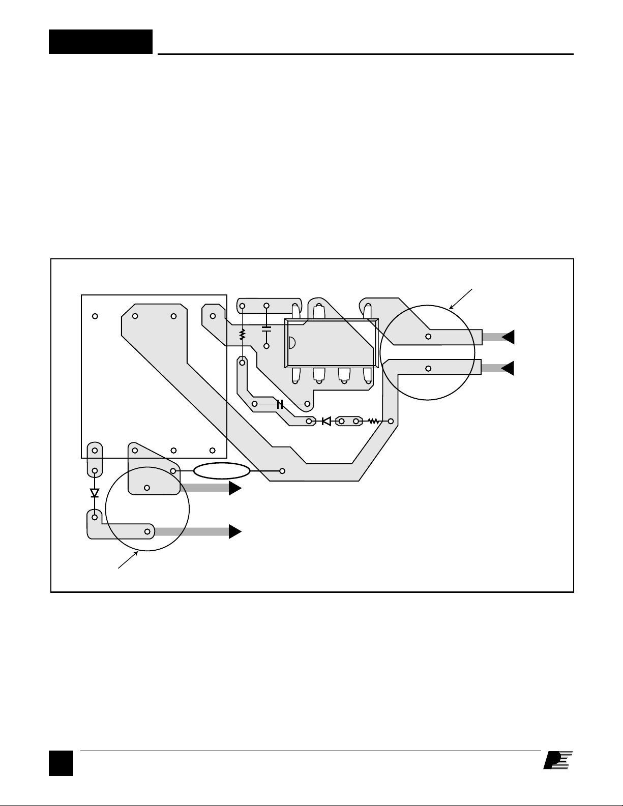
Layout considerations
Primary Side Connections
As the SOURCE pins in a LinkSwitch supply are switching
nodes, the copper area connected to SOURCE together with
C1, C2 and R1 (Figure 5) should be minimized, within the
thermal contraints of the design, to reduce EMI coupling.
The CONTROL pin capacitor C1 should be located as close as
possible to the SOURCE and CONTROL pins.
To minimize EMI coupling from the switching nodes on the
primary to both the secondary and AC input, the LinkSwitch
should be positioned away from the secondary of the transformer
and AC input.
Routing the primary return trace from the transformer primary
around LinkSwitch and associated components further reduces
coupling.
Y capacitor
If a Y capacitor is required, it should be connected close to the
transformer secondary output return pin(s) and the primary
bulk capacitor negative return. Such placement will maximize
the EMI benefit of the Y capacitor and avoid problems in
common-mode surge testing.
Control Pin Capacitor – C1
Capacitor C1 is used during start-up to power LinkSwitch and
sets the Auto-Restart frequency. For designs that have a battery
load this component should have a value of 0.22 µF and for
resistive loads a value of 1 µF. This ensures there is sufficient
time during start-up for the output voltage to reach regulation.
Any capacitor type is acceptable with a voltage rating of 10 V
or above.
Feedback Resistor – R1
The value of R1 is selected to give a feedback current into the
CONTROL pin of approximately 2.3 mA at the peak output
power point of the supply. The actual value depends on the V
OR
selected during design. Any 1%, 0.25 W resistor is suitable.
Output Diode – D2
Either PN fast, PN ultra fast or Schottky diodes can be used
depending on the efficiency target for the supply, Schottky
diodes giving higher efficiency then PN diodes. The diode
voltage rating should be sufficient to withstand the output
Quick Design Checklist
As with any power supply design, all LinkSwitch designs
should be verified on the bench to make sure that component
specifications are not exceeded under worst case conditions.
Note: In a LinkSwitch circuit, the SOURCE is a switching node.
This should be taken into consideration during testing.
Oscilloscope measurements should be made with probe
grounded to DC voltages such as primary return or DC rail but
not to SOURCE. Power supply input voltage should always be
supplied using an isolation transformer. The following minimum
set of tests is strongly recommended:
1. Maximum drain voltage – Verify that V
does not exceed
DSS
675 V at highest input voltage and peak output power.
2. Maximum drain current – At maximum ambient temperature,
maximum input voltage and peak output power, verify drain
current waveforms at start-up for any signs of transformer
saturation and excessive leading edge current spikes.
F
9
9/02
Page 10
LNK501
LinkSwitch has a minimum leading edge blanking time of
200 ns to prevent premature termination of the on-cycle.
Verify that the leading edge current spike event is below
current limit at the end of the 200 ns blanking period.
3. Thermal check – At peak output power, minimum input
voltage and maximum ambient temperature, verify that the
temperature specifications are not exceeded for LinkSwitch,
transformer, output diode and output capacitors. Enough
thermal margin should be allowed for part-to-part variation
of the R
of LinkSwitch as specified in the data sheet.
DS(ON)
Under low line, peak power, a maximum LinkSwitch
SOURCE pin temperature of 100 °C is recommended to
allow for these variations.
C
4. Centered output characteristic – Using a transformer with
nominal primary inductance and at an input voltage midway
between low and high line, verify that the peak power point
occurs at the desired nominal output current, with the correct
output voltage. If this does not occur then the design should
be refined to ensure the overall tolerance limits are met.
Design Tools
Up to date information on design tools can be found at the
Power Integrations Web site: www.powerint.com.
Input Filter
Capacitor
S
LinkSwitch
D
+
HV DC
Input
-
Transformer
Y1-
Capacitor
-
DC Out
+
Output
Capacitor
Figure 11. Recommended Circuit Board Layout for LinkSwitch using P Package.
SSSS
PI-2900-070202
10
F
9/02
Page 11
LNK501
ABSOLUTE MAXIMUM RATINGS
DRAIN Voltage ........................................ -0.3 V to 700 V
DRAIN Peak Current .............................................400 mA
CONTROL Voltage ..................................... - 0.3 V to 9 V
CONTROL Current (not to exceed 9 V)................100 mA
Storage Temperature ................................-65 °C to 150 °C
Operating Junction Temperature
Lead Temperature
(3)
................................................ 260 °C
(2)
...........-40 °C to 150 °C
THERMAL IMPEDANCE
Thermal Impedance: P/G Package:
(θJA) .............. 70 °C/W
(1)
(θJC)
................................. 11 °C/W
(2)
, 55 °C/W
Conditions
Parameter
Symbol
(Unless Otherwise Specified)
SOURCE = 0 V; TJ = -40 °C to 125 °C
See Figure 12
(1,4)
Notes:
1. All voltages referenced to SOURCE, T
= 25 °C.
A
2. Normally limited by internal circuitry.
3. 1/16" from case for 5 seconds.
4. Maximum ratings specified may be applied, one at a time,
without causing permanent damage to the product.
Exposure to Absolute Maximum Rating conditions for
extended periods of time may affect product reliability.
Notes:
(3)
1. Measured on the SOURCE pin close to plastic interface.
2. Soldered to 0.36 sq. inch (232 mm2), 2 oz. (610 gm/m2) copper clad.
3. Soldered to 1 sq. inch (645 mm2). 2 oz. (610 gm/m2) copper
clad.
Min Typ Max
Units
CONTROL FUNCTIONS
Switching
Frequency
Low Switching
Frequency
f
OSC(LOW)
Duty Cycle at
Low Switching
DC
Frequency
Low Frequency
Duty Cycle Range
Maximum
Duty Cycle
PWM
DC
DC
DC
Gain
CONTROL Pin
Current at 30%
Duty Cycle
CONTROL Pin
Voltage
V
f
OSC
LF
(RANGE)
MAX
REG
I
DCT
C(IDCT)
IC = I
Duty Cycle = DC
, TJ = 25 °C
DCT
LF
TJ = 25 °C
Frequency Switching from f
f
OSC(LOW)
Frequency = f
, TJ = 25 °C
, TJ = 25 °C
OSC(LOW)
IC = 1.5 mA
IC = I
, TJ = 25 °C
DCT
TJ = 25 °C
See Figure 4
IC = I
DCT
OSC
to
38 42 46
26 30 34
2.4 3.8 5.2
1.8 3.15 4.5
74 77 80
-0.45 -0.35 -0.25
2.24 2.30 2.36
5.5 5.75 6
kHz
kHz
%
%
%
%/µA
mA
V
Dynamic
Impedance
Z
C
IC = I
, TJ = 25 °C
DCT
60 90 120
9/02
Ω
F
11
Page 12
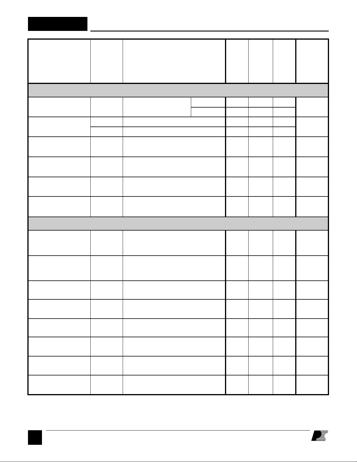
LNK501
Parameter
SHUTDOWN/AUTO-RESTART
Symbol
SOURCE = 0 V; TJ = -40 °C to 125 °C
Conditions
(Unless Otherwise Specified)
See Figure 12
Min Typ Max
Units
CONTROL Pin
Charging Current
Control/Supply/
Discharge Current
Auto-restart
Threshold Voltage
Auto-restart
Hysteresis Voltage
V
Auto-restart
Duty Cycle
Auto-restart
Frequency
CIRCUIT PROTECTION
Self-protection
Current Limit
I2 f Coefficient
Current Limit at
Auto-restart
Power Up Reset
Threshold Voltage
V
I
C(CH)
I
CD1
I
CD2
V
C(AR)
C(AR)hyst
DC
(AR)
f
(AR)
I
LIM
2
I
f
I
LIM(AR)
C(RESET)
VC = 0 V
TJ = 25 °C
VC = 5.15 V
Output MOSFET Enabled
Output MOSFET Disabled
Short circuit applied at
power supply output
Short circuit applied at power supply
output, C1 = 0.22 µF (See Figure 12)
TJ = 25 °C
di/dt = 90 mA/µs
See Note C
TJ = 25 °C
di/dt = 90 mA/µs
See Notes C, D
TJ = 25 °C
IC = I
CD1
-4.5 -3.25 -2
-2.3 -1.3 -0.3
0.95 1.06 1.14
0.7 0.9 1.1
5.6
0.9
8
300
241 254 267
2547 2710 2873
158
1.5 2.75 4.0
mA
mA
V
V
%
Hz
mA
A2Hz
mA
V
Leading Edge
Blanking Time
Current Limit
Delay
Thermal Shutdown
Temperature
Thermal Shutdown
Hysteresis
F
12
9/02
t
t
LEB
IL(D)
TJ = 25 °C
IC = I
DCT
TJ = 25 °C
IC = I
DCT
200 300
100
125 135
70
ns
ns
°C
°C
Page 13
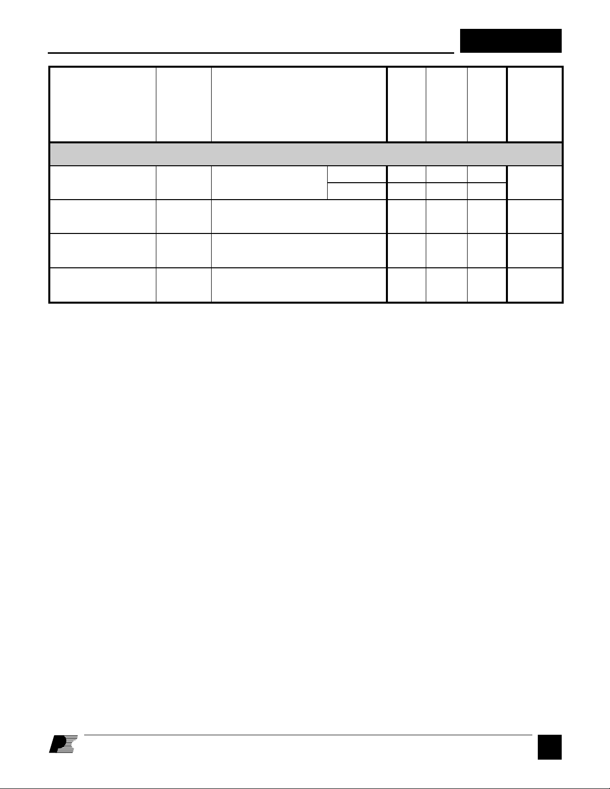
Parameter
OUTPUT
Symbol
Conditions
(Unless Otherwise Specified)
SOURCE = 0 V
; T
= -40 °C to 125 °C
J
See Figure 12
LNK501
Min Typ Max
Units
ON-State
Resistance
OFF-State
Current
Breakdown
Voltage
DRAIN Supply
Voltage
R
BV
DS(ON)
I
DSS
DSS
ID = 25 mA
TJ = 25 °C
T
J
See Note B, VC = 6.2 V
VD = 560 V, TA = 125 °C
See Note B
VC = 6.2 V, TA = 25 °C
See Note E
= 100 °C
700
36 50
28 32
42 48
50
Ω
µA
V
V
NOTES:
A. For specifications with negative values, a negative temperature coefficient corresponds to an increase in magnitude with
increasing temperature, and a positive temperature coefficient corresponds to a decrease in magnitude with increasing
temperature.
B. Breakdown voltage may be checked against minimum BV
exceeding minimum BV
C. IC is increased gradually to obtain maximum current limit at di/dt of 90 mA/µs. Increasing IC further would terminate the cycle
through duty cycle control.
D. This parameter is normalized to I
E. It is possible to start up and operate
current is reduced, which affects start-up time, auto-restart frequency, and auto-restart duty cycle. Refer to the characteristic
graph on CONTROL pin charge current (IC) vs. DRAIN voltage (Figure 13) for low voltage operation characteristics.
DSS
.
to correlate to power supply output current (it is multiplied by I
DCT
LinkSwitch
at DRAIN voltages well below 36 V. However, the CONTROL pin charging
specification by ramping the DRAIN pin voltage up to but not
DSS
(nominal)/I
DCT
DCT
).
9/02
F
13
Page 14
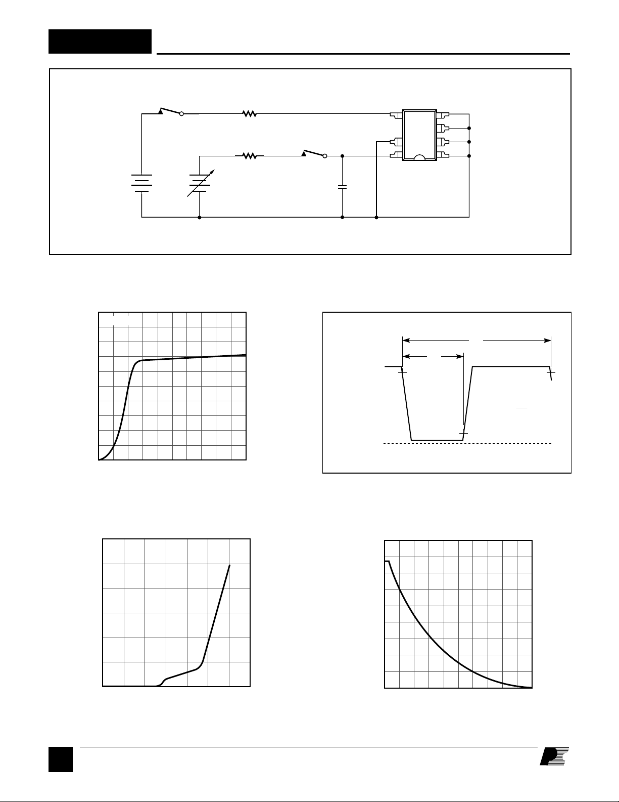
LNK501
90
50
60
70
80
0
2.15 2.25 2.35 2.45 2.55 2.65
Control Pin Current (mA)
Duty Cycle (%)
PI-2902-071602
20
10
40
30
S1
40 V
Figure 12. LinkSwitch General Test Circuit.
2
VC = 5.15 V
1.6
1.2
40 V
750 Ω
10 kΩ
PI-2901-071602
S2
0.22 µF
HV
LinkSwitch
D
S
C
90%
S
S
S
S
PI-2894-062802
t
2
t
1
90%
0.8
CONTROL Pin
0.4
Charging Current (mA)
0
0 20 40 60 80 100
DRAIN Voltage (V)
Figure 13. IC vs. DRAIN Voltage.
120
100
80
60
40
20
Control Pin Current (mA)
0
0.0 2.0 4.0 8.06.0 10.0 12.0 14.0
Control Pin Voltage (V)
Figure 15. CONTROL Pin I-V Characteristic.
14
F
9/02
PI-2895-062802
DRAIN
VOLTAGE
10%
0 V
Figure 14. Duty Cycle Measurement.
Figure 16. Duty Cycle vs. CONTROL Pin Current.
D =
t
1
t
2
PI-2048-050798
Page 15
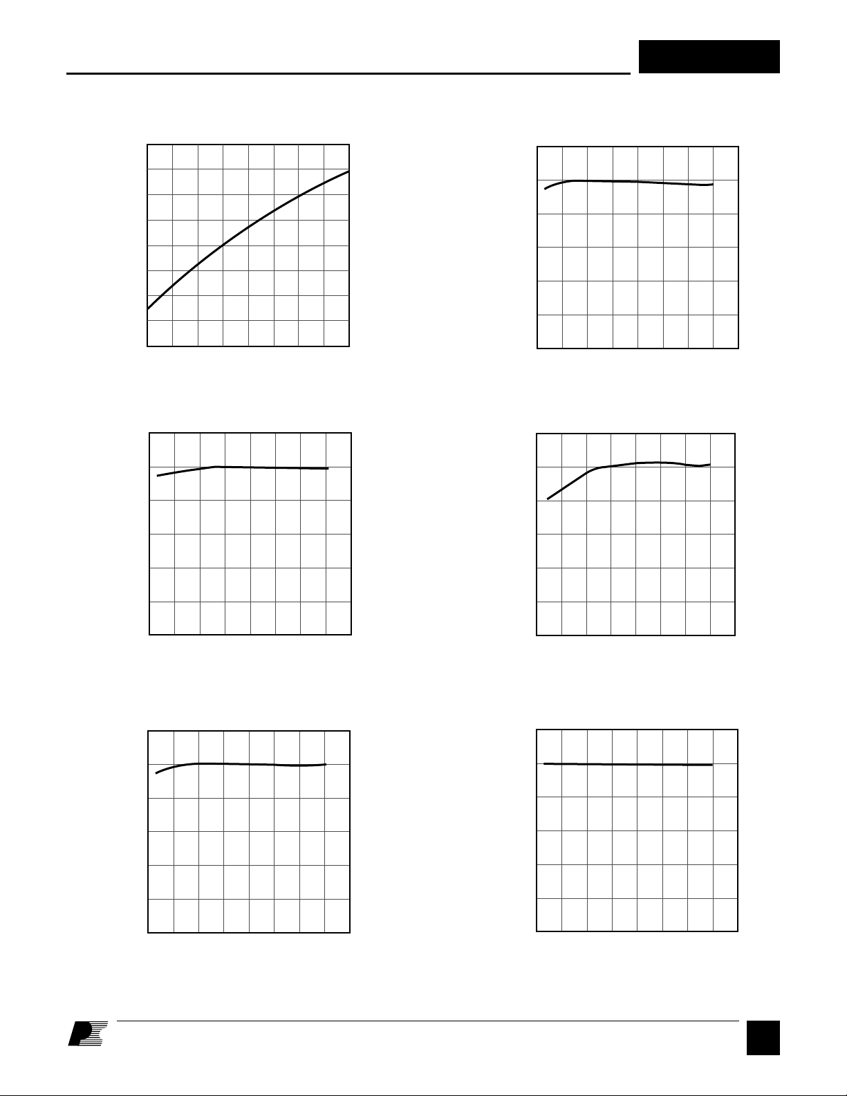
Typical Performance Characteristics
1.2
1
0.8
0.4
0.6
0.2
0
-50 0 50 100 150
Temperature (°C)
PI-2899-062802
PWM Gain (Normalized for 25 °C)
1.2
0.8
1.0
0.0
-50 -25 0 25 7550 100 150125
Junction Temperature (°C)
I
2
f Coefficient
(Normalized for 25
°C)
PI-2910-071602
0.2
0.6
0.4
LNK501
1.1
1.0
Breakdown Voltage
(Normalized to 25 °C)
0.9
-50 -25 0 25 50 75 100 125 150
Junction Temperature (°C)
Figure 17. Breakdown Voltage vs. Temperature.
1.200
1.000
°C)
0.800
0.600
PI-2213-012301
PI-2897-062802
1.200
1.000
°C)
0.800
0.600
0.400
Switching Frequency
(Normalized for 25
0.200
0.000
-50 0 50 100 150
Junction Temperature (°C)
Figure 18. Switching Frequency vs. Temperature.
PI-2896-062802
0.400
Current Limit
(Normalized for 25
0.200
0.000
-50 -25 0 25 50 75 100 125 150
Junction Temperature (°C)
Figure 19. Current Limit vs. Temperature.
1.200
1.000
0.800
0.600
0.400
(Normalized for 25 °C)
0.200
DCT
I
0.000
-50 0 50 100 150
Junction Temperature (°C)
Figure 21. I
vs. Temperature.
DCT
PI-2898-062802
2
Figure 20. I
f Coefficient vs. Temperature.
Figure 22. PWM Gain vs. Temperature.
9/02
F
15
Page 16
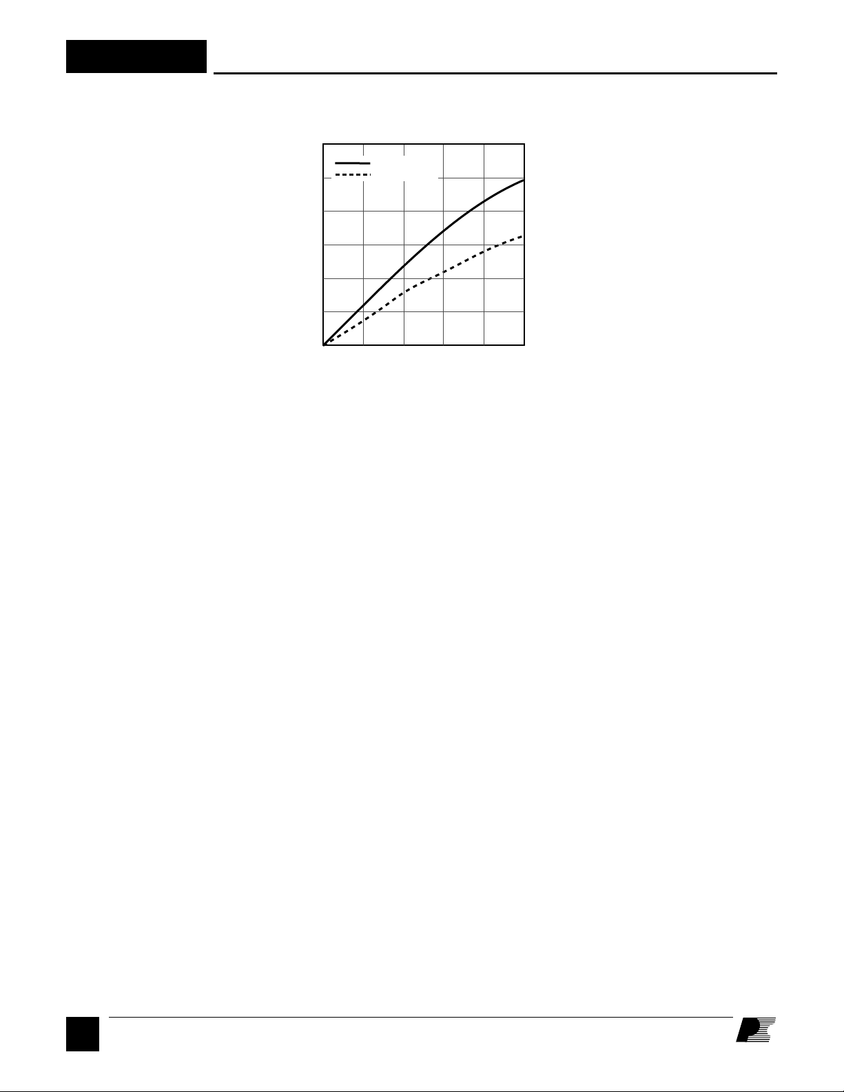
LNK501
Typical Performance Characteristics (cont.)
300
T
=25 °C
CASE
=100 °C
T
250
200
150
100
Drain Current (mA)
50
0
0246810
Figure 23. Output Characteristics (DRAIN Current vs.
DRAIN Voltage.
CASE
Drain Voltage (V)
PI-2221-031401
16
F
9/02
Page 17
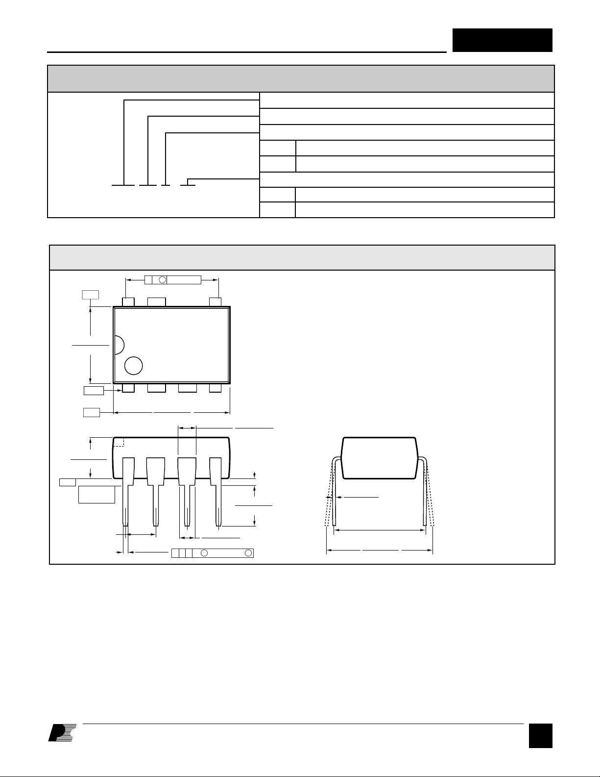
PART ORDERING INFORMATION
LNK 501 G - TL
D S
.004 (.10)
⊕
-E-
.245 (6.22)
.255 (6.48)
Pin 1
-D-
.128 (3.25)
.132 (3.35)
-TSEATING
PLANE
.100 (2.54) BSC
.375 (9.53)
.385 (9.78)
.014 (.36)
.022 (.56)
T E D S
⊕
.048 (1.22)
.053 (1.35)
.010 (.25) M
LinkSwitch
Product Family
Series Number
Package Identifier
G Plastic Surface Mount DIP
P Plastic DIP
Package/Lead Options
Blank Standard Configuration
TL Tape & reel in 1000 pc multiples, G package only
DIP-8B
Notes:
1. Package dimensions conform to JEDEC specification
MS-001-AB (Issue B 7/85) for standard dual-in-line (DIP)
package with .300 inch row spacing.
2. Controlling dimensions are inches. Millimeter sizes are
shown in parentheses.
3. Dimensions shown do not include mold flash or other
protrusions. Mold flash or protrusions shall not exceed
.006 (.15) on any side.
4. Pin locations start with Pin 1, and continue counter-clock wise to Pin 8 when viewed from the top. The notch and/or
dimple are aids in locating Pin 1. Pin 6 is omitted.
5. Minimum metal to metal spacing at the package body for
the omitted lead location is .137 inch (3.48 mm).
6. Lead width measured at package body.
.057 (1.45)
.063 (1.60)
(NOTE 6)
.015 (.38)
MINIMUM
.125 (3.18)
.135 (3.43)
7. Lead spacing measured with the leads constrained to be
perpendicular to plane T.
.010 (.25)
.015 (.38)
.300 (7.62) BSC
(NOTE 7)
.300 (7.62)
.390 (9.91)
LNK501
P08B
PI-2551-070302
9/02
F
17
Page 18
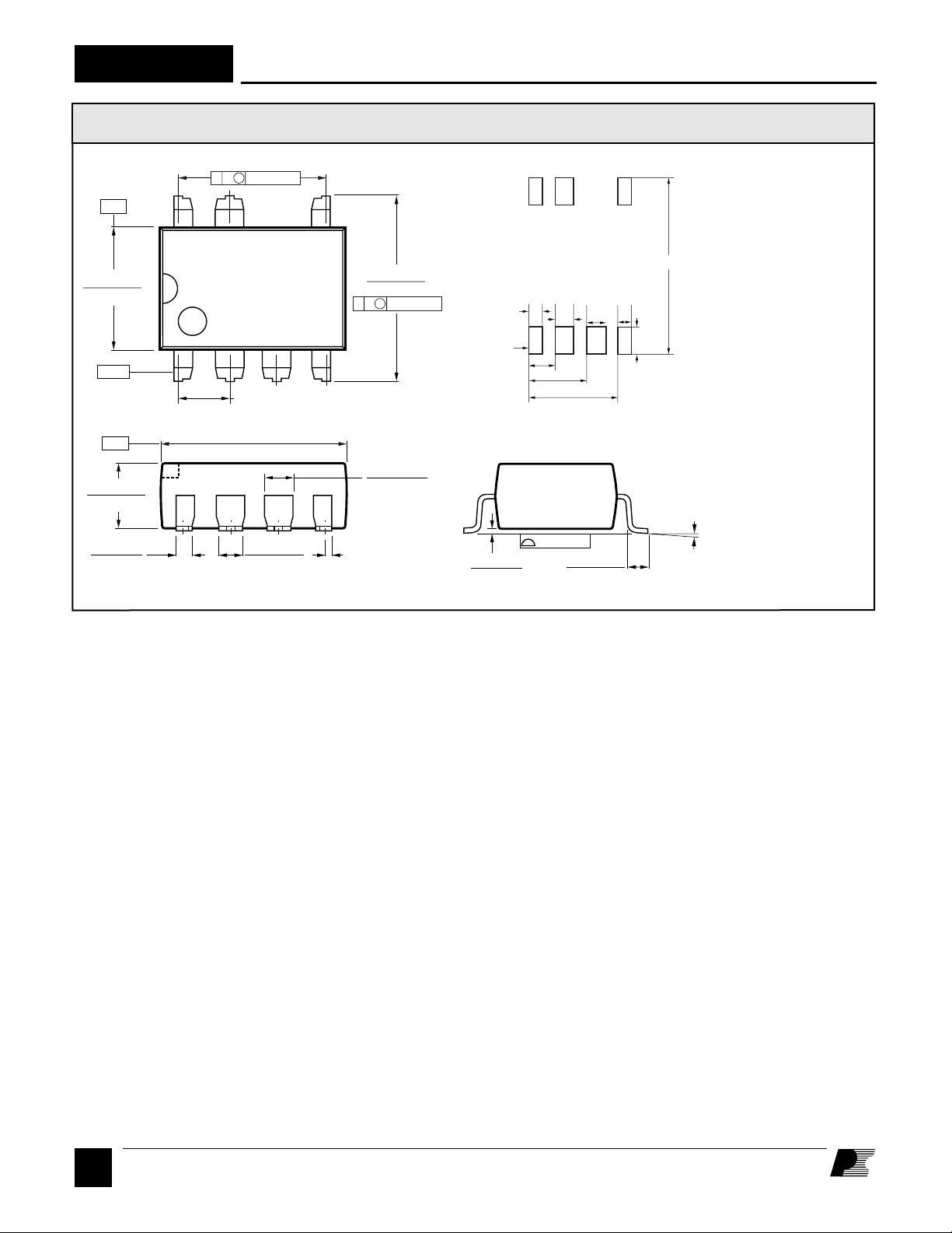
LNK501
SMD-8B
-E-
.245 (6.22)
.255 (6.48)
Pin 1
-D-
.128 (3.25)
.132 (3.35)
.032 (.81)
.037 (.94)
D S
.004 (.10)
⊕
.100 (2.54) (BSC)
.375 (9.53)
.385 (9.78)
.048 (1.22)
.053 (1.35)
.372 (9.45)
.388 (9.86)
E S
⊕
.057 (1.45)
.063 (1.60)
(NOTE 5)
.009 (.23)
.010 (.25)
.046
.060
Pin 1
.086
.186
.286
Solder Pad Dimensions
.004 (.10)
.004 (.10)
.012 (.30)
.036 (0.91)
.044 (1.12)
.060
.046
.080
Notes:
1. Controlling dimensions are
inches. Millimeter sizes are
shown in parentheses.
2. Dimensions shown do not
include mold flash or other
protrusions. Mold flash or
.420
protrusions shall not exceed
.006 (.15) on any side.
3. Pin locations start with Pin 1,
and continue counter-clock
Pin 8 when viewed from the
top. Pin 6 is omitted.
4. Minimum metal to metal
spacing at the package body
for the omitted lead location
is .137 inch (3.48 mm).
5. Lead width measured at
package body.
6. D and E are referenced
datums on the package
body.
°
°
8
0 -
G08B
PI-2546-081601
18
F
9/02
Page 19

LNK501
9/02
F
19
Page 20

LNK501
Revision
D
E
Notes
1) Final release data sheet
1) Enhanced tolerance with optocoupler designs
Date
7/02
8/02
2) Updated P and G packages thermal impedance
1) Corrected minor errors in text and figures
F
9/02
2) Updated Figure 6 and text description
LIFE SUPPORT POLICY
POWER INTEGRATIONS' PRODUCTS ARE NOT AUTHORIZED FOR USE AS CRITICAL COMPONENTS IN LIFE SUPPORT DEVICES OR
SYSTEMS WITHOUT THE EXPRESS WRITTEN APPROVAL OF THE PRESIDENT OF POWER INTEGRATIONS, INC. As used herein:
1. Life support devices or systems which, (a) are intended for surgical implant into the body, or (b) support or sustain life, and whose failure to perform, when
properly used in accordance with instructions for use provided in the labeling, can be reasonably expected to result in a significant injury to the user.
2. A critical component is any component of a life support device or system whose failure to perform can be reasonably expected to cause the failure of the life
support device or system, or to affect its safety or effectiveness.
For the latest updates, visit our Web site: www.powerint.com
Power Integrations reserves the right to make changes to its products at any time to improve reliability or manufacturability.
Power Integrations does not assume any liability arising from the use of any device or circuit described herein, nor does it
convey any license under its patent rights or the rights of others.
The products and applications illustrated herein may be covered by one or more U.S. and foreign patents or potentially by
pending U.S. and foreign patent applications assigned to Power Integrations. A complete list of Power Integrations’ patents
may be found at www.powerint.com.
The PI Logo,
PI Expert
WORLD HEADQUARTERS
AMERICAS
Power Integrations, Inc.
5245 Hellyer Avenue
San Jose, CA 95138 USA
Main: +1 408-414-9200
Customer Service:
Phone: +1 408-414-9665
Fax: +1 408-414-9765
e-mail: [email protected]
CHINA
Power Integrations
International Holdings, Inc.
Rm# 1705, Bao Hua Bldg.
1016 Hua Qiang Bei Lu
Shenzhen Guangdong, 518031
China
Phone: +86-755-8367-5143
Fax: +86-755-8377-9610
e-mail: [email protected]
TOPSwitch, TinySwitch
and
EcoSmart
are registered trademarks of Power Integrations, Inc.
is a trademark of Power Integrations, Inc. ©Copyright 2002, Power Integrations, Inc.
EUROPE & AFRICA
Power Integrations (Europe) Ltd.
Centennial Court
Easthampstead Road
Bracknell
Berkshire, RG12 1YQ
United Kingdom
Phone: +44-1344-462-300
Fax: +44-1344-311-732
e-mail: [email protected]
KOREA
Power Integrations
International Holdings, Inc.
8th Floor, dongSung Building,
17-8 Yoido-dong, Youngdeungpo-gu,
Seoul, 150-874, Korea
Phone: +82-2-782-2840
Fax: +82-2-782-4427
e-mail: [email protected]
SINGAPORE
Power Integrations, Singapore
51 Goldhill Plaza #16-05
Republic of Singapore 308900
Phone: +65-6358-2160
Fax: +65-6358-2015
e-mail: [email protected]
JAPAN
Power Integrations, K.K.
Keihin-Tatemono 1st Bldg.
12-20 Shin-Yokohama 2-Chome
Kohoku-ku, Yokohama-shi,
Kanagawa 222-0033, Japan
Phone: +81-45-471-1021
Fax: +81-45-471-3717
e-mail: [email protected]
TAIWAN
Power Integrations
International Holdings, Inc.
17F-3, No. 510
Chung Hsiao E. Rd.,
Sec. 5,
Taipei, Taiwan 110, R.O.C.
Phone: +886-2-2727-1221
Fax: +886-2-2727-1223
e-mail: [email protected]
INDIA (Technical Support)
Innovatech
#1, 8th Main Road
Vasanthnagar
Bangalore, India 560052
Phone: +91-80-226-6023
Fax: +91-80-228-9727
e-mail: [email protected]
APPLICATIONS HOTLINE APPLICATIONS FAX
World Wide +1-408-414-9660 World Wide +1-408-414-9760
F
20
9/02
 Loading...