

Page 1
Application Note AN-69
LinkSwitch-4 Family
Design Guide and Considerations
Introduction
The LinkSwitch™-4 family of ICs dramatically simplies low power
CV/CC charger/adapter design by eliminating an optocoupler and
secondary control circuitry. The LinkSwitch-4 family adaptive BJT drive
technology uses combined base and emitter switching to boost switching
performance and deliver higher efciency, wider Reverse Bias Safe
Operating Area (RBSOA) margin and the exibility to accommodate a
wide range of low cost BJT. The device incorporates a multimode PWM
/ PFM controller with quasi-resonant switching to maximize the efciency,
meets <30 mW no-load and at same time maintains fast transient
response greater than 4.3 V with a load change from 0% to 100%.
Advanced Performance Features
• Dynamic base drive technology provides exibility in choice of BJT
transistor by dynamically optimizing BJT switching characteristics
• Extends RBSOA of BJT
• Dramatically reduces sensitivity to BJT gain
• Compensates for transformer inductance tolerances
• Compensates for input line voltage variations
• Compensates for cable voltage drop
• Compensates for external component temperature variations
• Very accurate IC parameter tolerances using proprietary trimming
technology
• Frequency up to 65 kHz to reduce transformer size
• The minimum peak current is xed to improve transient load
response
Advanced Protection/Safety Features
• Single fault output overvoltage and short-circuit
• Over-temperature protection
EcoSmart™ – Energy Efcient
• Meets DoE 6 and CoC V5 2016 via an optimized quasi-resonant
switching PWM / PFM control
• No-load consumption of <30 mW at 230 VAC input
Green Package
• Halogen free and RoHS compliant package
Applications
• Chargers for cell/cordless phones, PDAs, MP3/portable audio
devices, adapters, etc.
LinkSwitch-4 Family
There are four main family groups covering a power range of nominally
2 W to 18 W and they come in either a SOT23-6 or SO-8 package.
Groups are further subdivided by cable drop compensation levels of
0%, 3% and 6%.
LNK43xxx and LNK4x15D devices have an enhanced base drive
optimization for reduced BJT losses. For example, the LNK4322S can
output 5 W using a TO92 13003 BJT instead of a TO251 13005 and
remain thermally safe. The LNK43x3 devices also include a debounce
delay after a low output voltage is detected to prevent false UVP
foldback being triggered in noisy environments.
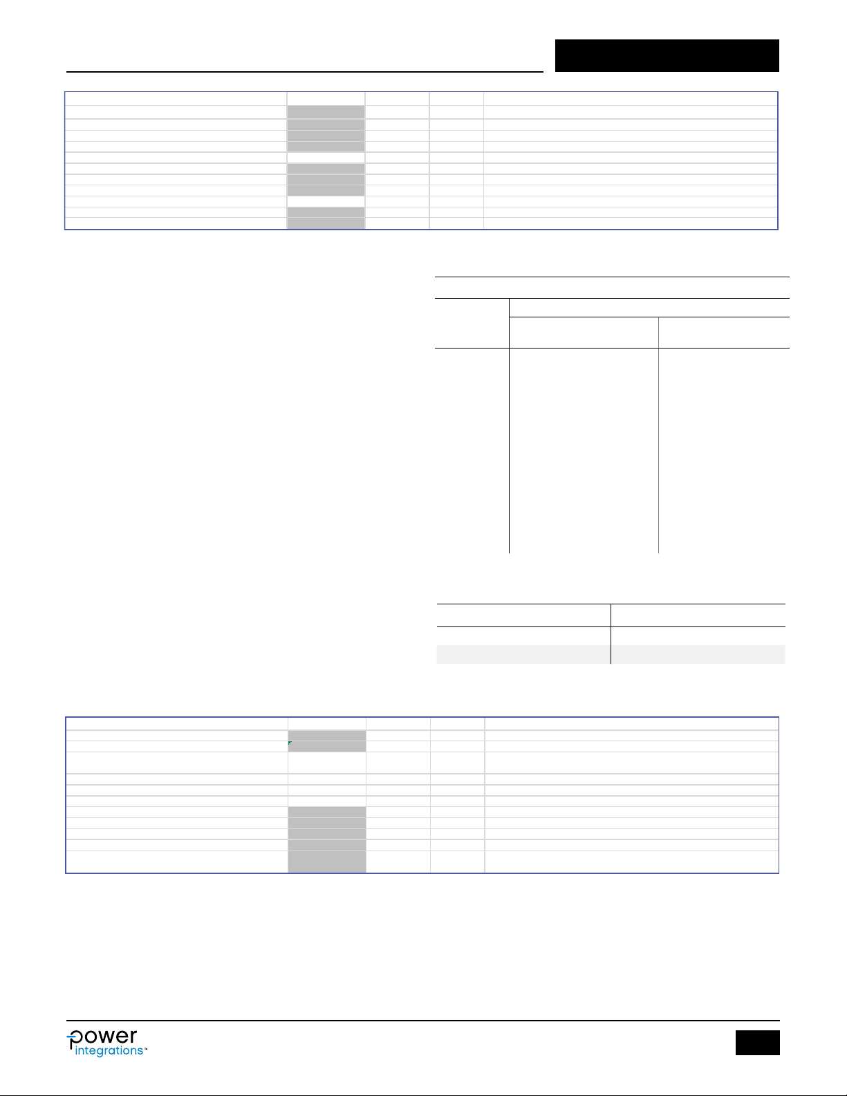
Output Power Table
8
FB
7
GND
6
GND
5
ED
85 - 265 VAC
5
Open Frame
S Package (SOT-23-6)
FB
GND
ED
8
FB
7
GND
6
GND
5
ED
Adapter
61
CS
52
VCC
43
BD
PI-7673-061516
1
2
Product
3,4
Features
LNK43x2S 13003 Drive 5 W
LNK40x2S STD 6.5 W
LNK40x3S STD 8 W
LNK4323S STD 8 W
LNK40x3D STD 10 W
LNK4323D STD 10 W
LNK40x4D STD 15 W
LNK4114D Easy Start 15 W
LNK4214D Easy Start + Constant Power 15 W
LNK4115D Easy Start 18 W
LNK4215D Easy Start + Constant Power 18 W
Table 1. LinkSwtich-4 Selection Table Based on Output Power.
D Package (SO-8)
(LNK40x3D, LNK4323D)
1
CS
2
VCC
3
SBD
4
BD
D Package (SO-8)
(LNK40x4D, LNK4114D, LNK4214D,
LNK4115D, LNK4215D)
1
CS
2
VCC
3
BD
4
SBD
Figure 1. LinkSwitch-4 Packages.
Note that the LNK4xx3D and LNK4xx4D SO-8 packages have the
SUPPLEMENTARY BASE DRIVE (SBD) pin and BASE DRIVE (BD) pins
swapped. This is to avoid problems with charger/adapter reliability.
The 10 W rated LNK40X3D would otherwise work in a 15 W LNK40X4D
design and may pass production nal test, but it would be overstressed and probably result in eld failures.
www.power.com October 2017
Page 2
Application Note AN-69
Scope
This application note is intended for engineers designing an isolated
AC-DC yback power supply using the LinkSwitch-4 family of devices.
It provides guidelines to enable an engineer to quickly select key
components and to complete a suitable transformer design. To
simplify the task this application note refers directly to the PIXls
design spreadsheet, part of the PI Expert design software suite.
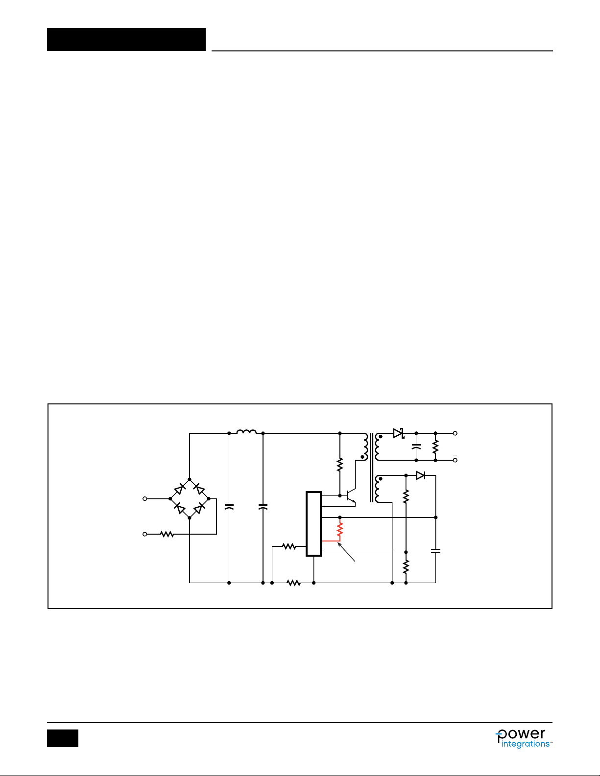
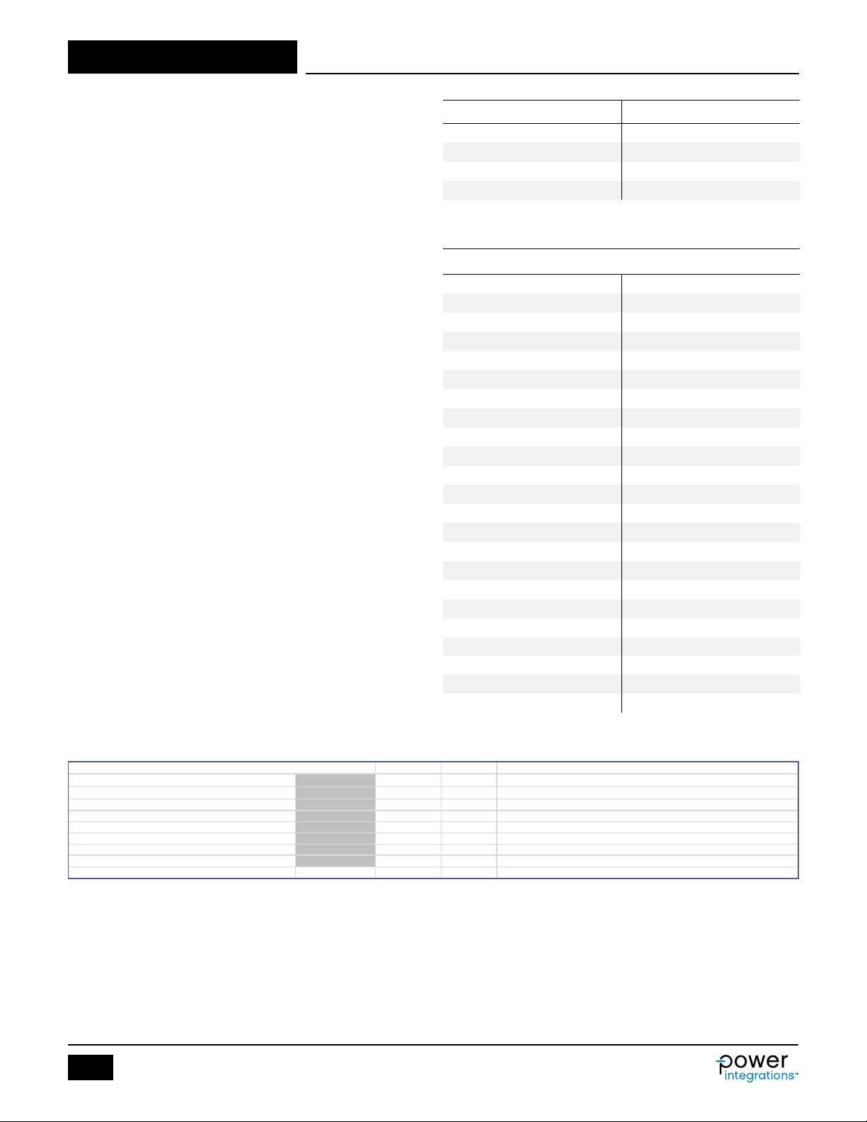
Basic Circuit Topology
The circuit in Figure 2 shows the basic topology of a yback power
supply designed using LinkSwitch-4. Because of the high-level
integration of LinkSwitch-4, far fewer design issues are left to be
addressed externally, resulting in one common circuit conguration
for all applications. For example, different output power levels may
require different values for some circuit components, but the circuit
topology stays unchanged. The exception to this is the optional SBD
resistor used with the SO-8 package parts. This increases the
available base drive current for higher power designs without
increasing the package power dissipation.
Schematic Features
• R
provides inrush current limiting at turn-on and under transient
IN
surge conditions.
• C
, C
and L
IN1
IN2
upon the AC supply, the capacitors also provide energy storage to
power the convertor during the valleys of the rectied AC.
• R
provides start-up current, which is amplied by the BJT to
HT
charge CVCC via the EMITTER DRIVER (ED) and VOLTAGE SUPPLY
(VCC) pins.
provide ltering to reduce switching noise impressed
FI LT
• R
converts the positive ramping primary current into a negative
CS
ramping voltage, which is monitored by the PRIMARY CURRENT
SENSE (CS) pin. It allows cycle-by-cycle peak primary current and
hence output power control, primary current limiting and, with the
transformer turns ratio, sets the maximum output current limit.
• R
reduces ESD susceptibility on all devices. Though highly
CS2
recommended, it is not strictly necessary on LNK40x2S parts.
On the remaining parts, it sets one of four minimum primary
current levels to control no-load behavior.
• R
is only used on SO-8 packaged parts. It allows for extra base
SBD
drive in higher power designs without increasing package dissipation
signicantly.
• T1 is the yback transformer. It stores energy in the primary wind-
ing and transfers it to the secondary and bias windings. There are
usually additional screen windings, not shown, to reduce EMI.
• The bias diode and C
• The bias winding is also used to measure the output voltage level
provide operational power to the controller IC.
VCC
on the secondary winding.
• For FEEDBACK (FB) pin positive voltage excursions, R
the turns ratio between the secondary and bias windings set the
, R
and
FB1
FB2
output voltage.
• For negative voltage excursions, the FEEDBACK pin is a virtual
earth amplier and is held at zero volts by sourcing current into
R
. This is translated internally into a voltage that represents the
FB1
HT voltage across C
detection, brown-out detection and BJT desaturation detection.
• R
is a dummy load for controlling no-load behavior.
OUT
. This is used to provide input undervoltage
IN2
In addition to this application note, you may also nd the LinkSwitch-4
Design Examples Reports (DER). Further details on downloading PI
Expert, Design Example Reports, and updates to this document can
be found at www.power.com.
D
BRIDGE
~
R
IN
Figure 2. Typical LinkSwitch-4 Circuit Topology.
D
OUT
T1
+
C
L
FILT
2 × R
HT
Q1
BD
C
IN1
C
IN2
LNK40x3D
R
CS2
R
CS
ED
VCC
SBD
CS
FB
GND
SBD pin only available
on SOP-8 package parts
R
SBD
OUT
PI-7962-052416
R
OUT
R
FB1
C
VCC
R
FB2
2
Rev. B 10/17
www.power.com
Page 3

Application NoteAN-69
Quick Start
To start immediately, use the following information to quickly design
the transformer and select the components for a rst prototype.
Only the information described below needs to be entered into the
PIXls spreadsheet gray cells in column [B]. Some gray cells have
entries in bold font, these contain drop down selections. If an invalid
selection is made, then Info or Warning text will appear in column [C]
and [D], a description of the error is displayed in column [H]. Other
parameters and component values will be automatically calculated.
References to spreadsheet cell locations are provided in square
brackets [cell reference].
The default design presented in a blank spreadsheet is for a 5 V, 2 A
adapter with 6% cable compensation and standard universal AC input
voltage range. All gray cells are blank except for those with bold text
drop down selections, which are set to the appropriate selections for
the default adapter. The default values are displayed in column [E]
and [F]. When an entry is made in a column [B] gray cell, its value is
transferred into the corresponding cell in columns [E] and [F] and
from there, used in the calculations.
It is only necessary to enter values into column [B] if they are
different to the default values in column [E].
• If a non-standard AC input voltage range is required, enter the
values for VAC
• Enter the nominal output voltage (at the end of the cable if
applicable), VO [B6].
• Entre the output diode forward volt drop if different to the
standard Schottky value, VD [B8].
• Enter the minimum required output current value, I
that cell [E10] is updated with a suggested minimum CC value for
ICC. See Figure 4.
• Enter the required CC limit, ICC [B10], if it is higher than the
suggested minimum I [E10]. See Figure 4.
• Enter an efciency estimate, η [B12]. Use the target gure from
the applicable efciency standard.
• Use the drop down selection menu in [B19] to select the desired
cable compensation. Output voltage at the PCB, VO_PCB, is now
given in [E7].
• The minimum recommended bulk capacitance value (C
given in [E13]. If a larger value, or standard values are to be used,
enter their total value into [B13].
• Using the value for ‘rated output power’ in cell [E11], use table 1
on page 1, to choose the correct LinkSwitch-4 device. Use the
drop down selection menu in [B18] to select that device.
• BJT types TS13003 and TS13005 are auto selected based on
output power. To use a different BJT, enter PART_NUMBER, HFE_
STARTUP (low current gain), HFE (high current gain) and VSWMAX
(V
) into [B24,B25,B26,B27].
CBO
• Use the drop down selection menu in [B35] to select ‘AUTO’. A
suitable core, bobbin and parameters will automatically be entered
into cells [E35 – E43].
• To optimize for efciency enter an alternative value for the
reected output voltage, VOR in [B49], the default is 100 V. While
trying different values, observe the changes in KCRMV [E65] and
aim to get between 0.95 and 0.98. At the same time ensure
MIN
, VAC
and fL into cells [B3, B4, B5] as required.
MAX
[B9]. Notice
O
+ C
IN1
IN2
) is
VCRMV-VMIN [E56-E57] is less than 15 V, but the higher VCRMV
the better. The spreadsheet will produce a reasonable solution if
VOR is left at the default 100 V.
• Fixing the number of secondary turns in [B50] while sweeping the
VOR value [B49] offers further optimization possibilities.
• The default primary inductance tolerance is 10%, an alternative
value can be entered in [B88]. Tighter tolerance allows better
average efciency across production.
• The default number of primary winding layers is 3 [E98], if the
primary current density [E103] is less than 3.8 Amps / mm2 it can
be reduced to 2 by an entry into [B98]. If greater than 10 Amps /
mm2, increase to 4 etc. The fewer layers the better for leakage
inductance and hence efciency.
• The default calculated number of turns for the bias winding, NB
[E105] is based on providing a no-load bias voltage, VB_NOLOAD
[E107] that achieves the lowest no-load power. However, start-up
may be compromised so enter a value between 8 and 9 into
VB_NOLOAD [B107]. NB will be recalculated; check the value of
VB_NOLOAD_MEASURED [E109] is between 8 and 9 V. If not,
adjust the value in [B107] and recheck.
• One secondary layer is optimal for efciency, but if the output
voltage is high resulting in the secondary wire being impractically
thin, DIAS [E120], then it can be increased by entering a value in
LS [B116]. The spreadsheet calculates for a triple insulated wire
size that will ll the bobbin width in an integer number of layers
given in [E116].
• For low voltage designs, particularly at higher powers and larger
cores, the wire thickness becomes impracticably thick to wind. By
winding the secondary with a number of parallel conductors, the
wire thickness is reduced to a practical value, also leakage
inductance is decreased which improves efciency. To use more
than one conductor, enter a value into Filars [B117] and recheck
the new calculated wire size, DIAS [E120].
• Enter a BJT voltage derating factor into SWITCH_DERATING
[B126] if other than 0.10 (10%) is required.
• Use the drop down selection menu in VCS_MIN [B135] to set the
minimum value of peak primary current at no-load. It is repre-
sented by the peak mV across RCS. For the LNK40X2S devices, only
88 mV should be selected and a 1 kW value be used for R
ltering. For other devices select the lowest value (56 mV) for the
CS2
for
rst iteration.
• If the application requires no-load to partial or full load transient
capability, where the output voltage must not fall below a minimum
value as in USB charger applications, check the value of CBIAS
[E138] if it is more than 2 mF, enter the value ‘2’ into [B138].
Check DELTA_BIAS [E139] is less than 1.6 V.
• Output capacitor calculation for starting up into a resistive load:
Use the drop down selection menu in LOAD_TYPE [B141] to select
‘Resistive Load’. The spreadsheet calculates the maximum value of
output capacitance the circuit will start up into i.e. before CBIAS
runs out of charge.
• For a CC load at start-up, use [B141] to select ‘CCLoad’. The
default start-up CC load current is 75% of IO, the rated output
current (not the CC limited value) if another value is specied,
enter it into ICC_STARTUP [B142].
• If the suggested output capacitance value needs to be rounded up
to a preferred value, enter this into COUT_FINAL [B145].
www.power.com
3
Rev. B 10/17
Page 4

Application Note AN-69
If no-load to partial or full load transient step is required as in USB
chargers:
• Enter the load step value into I_LOADSTEP [B148] if it is different
to the rated output current.
• Enter the minimum load voltage allowed during no-load to partial
or full load transient testing into V_UNDERSHOOT [B149].
• Check that FSW_NOLOAD value in [E154] is greater than FSW_
UNDERSHOOT in [E150]. If not, select a lower value for VCS_MIN
[B135], if already at the lowest setting or a LNK40x2S device is
being used, enter a lower value for R_PRELOAD [B152] untill the
condition is met.
• Check that the no-load power specication is met, P_NOLOAD_TO-
TAL [E174], if not select a higher value of VCS_MIN [B135] (not
LNK40X2S) and recheck that the FSW_
NOLOAD>FSWUNDERSHOOT and no-load power requirements are
met. If using a LNK40X2S, R_PRELOAD [B152] can be increased,
but no more than 2x.
If no transient step requirement:
• Select a value of VCS_MIN [B135] and R_PRELOAD [B153] that
gives a FSW_NOLOAD of between 1 kHz and 2 kHz and still meets
the no-load specication.
• Enter the maximum allowed start-up time into STARTUP_TIME
[B156] if it is not to be 1 second. Or enter a preferred value into
R_STARTUP [B157], a new value of the resultant startup time is
given in STARTUP_TIME_FINAL [E158].
Supplementary Base Drive
Resistor R
drive in higher power applications (7.5 W to 18 W). It should have a
is used on SO-8 packaged devices to provide extra base
SBD
value of between 390 W and 220 W for standard designs, or 120 W for
applications using the EasyStart feature. Refer to the ‘Design
Testing’ section to check that correct value has been selected.
Component values for the design are found in:
+ C
C
IN1
Selected device – [E20]
, CIN [E13]
IN2
Q1 BJT – [E24]
T1 Core - [E35]
T1 Bobbin – [C37]
T1 Primary turns – [E51]
T1 Primary layers – [E98]
T1 Primary wire diameter – [E101, E102]
T1 secondary turns – [E50]
T1 Secondary layers – [E116]
T1 Secondary lars – [E117]
T1 Secondary wire diameter – [E120, E121]
T1 Bias turns – [E106]
T1 Core gap – [E93]
C
, Bias capacitor value – [E138]
VCC
Total output capacitance C
Output capacitance ripple – [E81]
R
Dummy load – [E152]
OUT
RHT Start-up resistor – [E157]
R
Upper feedback resistor – [E161]
FB1
R
Lower feedback resistor – [E162]
FB2
RCS Current sense resistor – [E74]
R
Bias diode V
D
D
D
setting resistor – [E136]
CS2 VCSMIN
OUT VRRM
Peak current – [E79]
OUT
RMS current – [E780]
OUT
– [E129] usually 1N4148
RRM
– [E128]
, [E145]
OUT
Explore the spreadsheet for more informative data.
4
Rev. B 10/17
www.power.com
Page 5
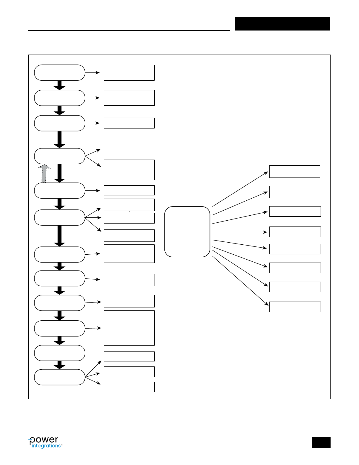
Step-by-Step Design Procedure
Application NoteAN-69
Specify Application
Parameters
Bulk Capacitor
Election
IC and BJT
Selection
Transformer Core,
Bobbin, Turns
Optimize Turns Ratio
for Efficiency
Resulting HT, Primary
and Secondary
Conditions
.
Customer / Data Sheet
Defined; Assumptions
Determines Minimum HT
Voltage at Full Load
Power Range, CDC
Core Type; Size ; Material
Calculations: Turns,
Primary Inductance,
Peak Current, etc
VOR, NS, N
Minimum HT Voltage,
Brown-Out HT Voltage
Peak Primary Current
Current Sense
Resistor Value
P
Testing and
Troubleshooting
Collector Voltage at
100%, 50%, 0% Load
Assess Switching
Frequency vs. Load
AUX Voltage vs. Load
Startup / Load Pull-Up
Secondary Waveform
Parameters
Transformer
Construction
Bias Winding
Parameters
Additional Parameters
No-Load Power Estimate
PCB Layout
Figure 3. Design Flow Char t.
Peak, RMS Secondary
Current and C
Ripple Current
Wire Gauge, Number of
Layers, Filars
Bias Turns for Required
Bias Voltage
Bias Capacitor
Output Capacitor
Loadstep Undershoot
Dummy Load
Start-Up
Feedback Resistors
Function Consideration
EMC Consideration
Thermal Consideration
OUT
Efficiency
No-Load Power
Ripple
Thermal
PI-7977-012417
www.power.com
5
Rev. B 10/17
Page 6
Application Note AN-69
P
V
2
22
c
m
General Guidance for Using the PIXls Design
Spreadsheet
Only the information described below needs to be entered into the
PIXls spreadsheet gray cells in column [B]. Some gray cells already
have entries in bold font, these contain drop down selections. If an
invalid selection is made, then Info or Warning text will appear in
column [C] and [D], a description of the error is displayed in column
[H]. Other parameters and component values will be automatically
calculated. References to spreadsheet cell locations are provided in
square brackets [cell reference].
The default design presented in a blank spreadsheet is for a 5 V, 2 A
adapter with 6% cable compensation and standard universal AC input
voltage range. All gray cells are blank except for those with bold text
drop down selections, which are set to the appropriate selections for
the default adapter. The default values are displayed in column [E]
and [F]. When an entry is made in a column [B] gray cell, its value is
transferred into the corresponding cell in columns [E] and [F] and
from there, used in the calculations.
Do not read off calculated component values etc, until all the data
has been entered.
It is only necessary to enter values into column [B] if they are
different to the default values in column [E].
Step 1 – Enter Application Variables VAC
V
, VD, IO, ICC, η
O
AC Input Voltage Range, VAC
Determine the input voltage from Table 2 for common choices, or
enter the application specication values into [B3, B4].
Nominal Input Voltage (VAC) VAC
100/115 85 132
230 195 265
Universal 85 265
Table 2. Standard Worldwide Input Line Voltage Ranges.
Note: For designs that have a DC rather than an AC input, enter the
values for minimum and maximum DC input voltages, V
V
[B58], directly into the grey override cell on the design spread-
MAX
sheet (see Figure 5).
Line Frequency, ƒ
Typical line frequencies are 50 Hz for universal or single 100 VAC,
L
60 Hz for single 115 VAC, and 50 Hz for single 230 VAC inputs. These
values represent typical, rather than minimum, frequencies. For most
applications this gives adequate overall design margin. To design for
the absolute worst case, or based on the product specications,
reduce these numbers by 6% (to 47 Hz or 56 Hz). For half-wave
rectication use F /2. For DC input enter the voltage directly into
cells, V
[B57] and V
MIN
MAX
[B58].
Nominal Output Voltage, VO (V)
For both CV/CC and CV only designs, V is the nominal output voltage
measured at the end of an attached cable carrying nominal output
current. The tolerance for the output voltage is ±5% (including initial
tolerance and over the data sheet junction temperature range).
Output Diode Forward Voltage Drop, VD (V)
Enter the average forward-voltage drop of the output diode. Use
0.4 V for a Schottky diode or 0.7 V for a PN-junction diode (if specic
diode data is not available). VD has a default value of 0.4 V.
MIN
, VAC
MAX
MIN
MIN
, VAC
VAC
[B57] and
MIN
MAX
MAX
, ƒL,
Minimum Required Output Current, I
This is the nameplate current and is the current that must be
O
(A)
supplied at the nameplate voltage, before the VI curve follows the
decreasing voltage CC characteristic. It is the output current level at
which efciency measurements are taken. See Figure 4.
V
OUT
100%
VO [B6]
I
[B10]
CC
I
O
0
Figure 4. VI Curve With Parameter Positions Identied.
[B9]
100%
PI-8108-092116
I
OUT
CC Mode Current Output Level, ICC (A)
In CC mode, the output current is regulated to the ICC value. There is
a 7% overall tolerance on the regulated value, so the spreadsheet
automatically defaults to setting this level to IO + 8%. It is possible
to set ICC to a higher level by entering a value into [B10], a higher
value will help start-up into CC and/or high capacitance loads. It is
recommended that ICC < IO+ 20% else efciency will be signicantly
reduced.
Power Supply Efciency, η
Enter the estimated efciency of the complete power supply, as
would be measured at the output cable end (if applicable). In
practice, use the applicable energy saving standard value. If the
completed power supply fails to meet this value of efciency, some
components may be over stressed, but as the design has failed the
efciency specication it will need modifying anyway, before being
accepted for production.
Total Input Capacitance, C
This is calculated from the maximum power drawn from the bulk
capacitors at VAC
(V
) at which the convertor will operate efciently, nominally 80 V,
MIN
and the line frequency (FL). The value calculated in [E13] - with [B13]
, the minimum allowable bulk capacitor voltage
MIN
IN
blank, is the minimum required capacitance. A higher value may be
entered into [B13] to round up to the nearest standard value, or
increase the operating efciency of the converter stage over the AC
input voltage range. The total value of CIN is then split into two
approximately equal values, C
It is advisable to make at least C
and C
IN1
IN2
a low ESR type.
IN2
, to provide the input pi lter.
The following equation may be used to calculate the minimum
capacitance required:
CC
IN IN
12
$
+
^
h
FVV
h
()
LMIN ACMIN MIN
arccos
O
^
2
##
V
-
MIN
#
ACMIN
#
h
-
Use higher values to allow for capacitor tolerance.
6
Rev. B 10/17
www.power.com
Page 7
Application NoteAN-69
ENTER APPLICATION VARIABLES
VACMAX
265 Volts Maximum AC Input Voltage
fL 50 Hertz AC Mains Frequency
VO 5.00 Volts Output Voltage at the end of the cable
VO_PCB 5.30 Volts Output Voltage at PCB. Changes with cable compensation selection
VD 0.40 Volts Output Winding Diode Forward Voltage Drop
IO 2.00 Amps Full load rated current. Used for all waveshape related calculations.
ICC 2.16 Amps CC setpoint. Must be >= IO+7%. Affects Rc s.
PO 10.60 Watts Rated output power including cable drop compensation. Calculated from IO
n 0.80 %/100 Effic iency Estimate
ENTER LINKSWTCH-4 VARIABLES
LinkSwitch-4 LNK40X4D Select LNK-4
Cable drop compensation option 6% 6% Select level of cable drop compensation
DEVICE
Complete reference of select part number with the selected cable drop
compensation option
FSW 65000 Hertz LinkSwitch-4 typical switching frequency
ILIM_MAX 1.10 A Maximum emi tter pin sink current
Transistor
PART_NUMBER TS13005 Example transistor for the current application
HFE_STARTUP 12 Minimum DC current gain at no load and startup. Affects start-up delay
HFE 25 Minimum DC current gain for load transient
VSWMAX
700 Volts Switch Breakdown voltage
V_CGND_ON
BJT + LNK-4 on-state Collector to ground Voltage (3V if no better information
available)
VACMIN
CIN 20.0 uFarads Total input bulk Capacitance
Figure 5. Application Variables Section of the Design Spreadsheet.
Step 2 – Enter LinkSwitch-4 Selection
90 Volts Minimum AC Input Voltage
Output Power Table
Select the Cable Drop Compensation Option
Select the cable compensation option from the drop down selection
menu in [B19] to most closely match the percentage output voltage
drop in the output cable. For example, a 5 V, 2 A LNK40x4D design
with a cable impedance of 150 mW has a cable voltage drop of
-0.3 V. With a desired nominal output voltage of 5 V (at the end of
the cable), this represents a voltage drop of 6%. In this case, select
the +6% compensation, to give the smallest error. 0%, 3% or 6%
can be selected.
Selecting the Correct LinkSwitch-4 Part
Using the value for rated output power’ in cell [E11], use Table 1 on
page 1, to choose the correct LinkSwitch-4 device. Use the drop
down selection menu in [B18] to select that device. The full part
number is given in [E20].
The full load switching frequency of standard LinkSwitch-4 devices is
65 kHz.
Enter BJT selection
BJT types TS13003 (up to 5 W) and TS13005 (up to 18 W) are auto
LNK43x2S 13003 Drive 5 W
LNK40x2S STD 6.5 W
LNK40x3S STD 8 W
LNK4323S STD 8 W
LNK40x3D STD 10 W
LNK4323D STD 10 W
LNK40x4D STD 15 W
LNK4114D Easy Start 15 W
LNK4214D Easy Start + Constant Power 15 W
LNK4115D Easy Start 18 W
LNK4215D Easy Start + Constant Power 18 W
Table 3. Selection Table of LinkSwitch-4 Parts by Power and Maximum BJT
selected based on output power. There are 800 V and 900 V rated
Design title
Product
3,4
Features
Emitter Current (Primary Current).
TS13003 parts for special circumstances, such as snubberless design
or higher AC input voltage e.g. 420 VAC. To use a different BJT, enter
PART_NUMBER, HFE_STARTUP (low current gain), HFE (high current
gain) and VSWMAX (V
) into [B24, B25, B26, B27].
CBO
BJT Output Power
TS13005 Up to 15 W
TS13003 Up to 5 W
85 - 265 VAC
5
Adapter
1
Open Frame
2
Table 4. Recommended BJTs.
LNK4024D
3.0 Volts
Figure 6. LinkSwitch-4 and BJT Selection.
www.power.com
7
Rev. B 10/17
Page 8
Application Note AN-69
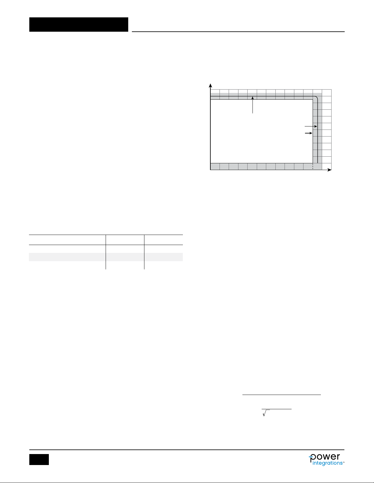
Core Type
EPC17 EPC17 Core Type
Custom Core (Optional)
If Custom core is used - Enter Part number here
Bobbin
P/N: BEPC-17-1110CPH
AE 0.23 cm^2 Core Effective Cross Sectional Area
LE 4.02 cm Core Effective Path Length
AL 1150 nH/T^2 Ungapped Core Effective Inductance
BW 9.55 mm Bobbin Physical Winding Width
M
0 mm Safety Margin Width (Half the Primary to Secondary Creepage Distance)
BWE
9.6 mm Effective Bobbin Width
ENTER TRANSFORMER CORE/CONSTRUCTION VARIABLES
Step 3 – Core and Bobbin Selection Based on Output
Power and Enter A
These symbols represent core effective cross-sectional area AE (cm2),
core effective path length LE (cm), core ungapped effective inductance
AL (nH/ Tu r n2), bobbin width BW (mm) and safety margin width M (mm).
Due to the small transformer size that results at these power levels,
triple insulated wire is generally used for the secondary, so Safety
Margin Width is not used and left set to the default ‘0’ setting. If the
Safety Margin method is preferred and standard wire used, enter the
safety margin width. The spreadsheet will double it and subtract it
from the bobbin width (BW) and give the effective bobbin width, or
winding width (BWE). Universal input designs typically require a total
margin of 6.2 mm, and a value of 3.1 mm entered into [B42]. The
spreadsheet uses the value of BWE to calculate the required wire diam-
eter to ll the available bobbin width to minimize leakage inductance.
For designs using triple-insulated wire it may still be necessary to
enter a small margin to meet required safety creepage distances.
Typically many bobbins exist for each core size, each with different
mechanical spacing. Refer to the bobbin data sheet or seek guidance
from your safety expert or transformer vendor, to determine the
requirement for your design. The margin reduces the available area
for windings, so margin construction may not be suitable for
transformers with smaller cores. If, after entering the margin, more
than three primary layers (L) are required, either select a larger core
or switch to a zero-margin design using triple-insulated wire.
If the drop down selection menu in [B35] is used and ‘AUTO’ selected,
the spreadsheet selects the smallest core size, by AE, that meets the
peak ux density limit. The user can select an alternative core from
drop down list of commonly available cores (shown in Table 6). Table 5
provides guidance on the power capability of specic core sizes.
If the user has a preferred core not in the list, then the appropriate
parameters can be entered into [B36 – B42].
, LE, AL, BW, M
E
Core Size Output Power Capability
EF12.6 3.3 W
EE13 3.3 W
EE16 6.1 W
EF20 10 W
Table 5. Output Power Capability of Commonly used Sizes in LinkSwitch-4
Designs.
Transformer Core Size
EE10 EF32
EF12.6 EFD15
EE13 EFD25
E24/25 EFD30
EE16 EI16
EE19 EI19
EE22 EI22
EEL16 EI25
EE16W EI28
EEL19 EI30
EEL22 EI35
EE25 EI40
EEL25 EPC17
EEL28 EPC19
EER28 EPC25
EER28L EPC30
EER35 ETD29
EER40 ETD34
EES16 ETD39
EF16 EE42/21/15
EF20 EE55/28/21
EF25 EF32
EF30
Table 6. List of Cores Provided in LinkSwitch-4 PIXls Spreadsheet.
Figure 7. Transformer Core Selection.
8
Rev. B 10/17
www.power.com
Page 9
Application NoteAN-69
MAIN OPTIMIZATION INPUTS
Turns and ratio
VOR 100.00 Volts Reflected Output Voltage. Use Goal Seek to get VCRMV to desired value.
NS
Number of Secondary Turns. Adjusting up or down along with VOR may improve
efficiency.
NP
105 Primary Winding Number of Turns
DC INPUT VOLTAGE PARAMETERS
VCRMV
94 Volts Vbulk at CRMV, at max LP tolerance. Higher value typically more efficient.
VMIN
Bulk cap "trough" voltage at VACMIN. Leave blank to calculate from capacitance
and load.
VMAX 375 Volts
Maximum DC Input Voltage
VBROWN
51
Volts
Bulk voltage it loses regulation
PRIMARY WAVEFORM PARAMETERS
F_RES 400 kHz Anticipated resonant frequency on the primary side (180<Ftrf<1200)
KCRMV 0.95 Ratio of primary switch off time to secondary conduction plus first valley time
IRMS 0.25 Amps Primary RMS Current (calculated at load=IO, VMIN)
IP 0.60 Amps Peak Primary Current (calculated at load=IO, VMIN)
IOCP
Pulse by pulse current limit. Appears during large load transients and brownout
operation.
IAVG 0.16 Amps Average Primary Current (calculated at load=IO, VMIN)
IP_CRMV 0.56 Amps Ipeak when Vin=Vcrm
F_CRMV 65000 Hz Fsw when Vin=Vcrm
FVMIN
62410 Hz Fsw at VMIN. If < 65kHz, is in frequency reduction mode
VCS_VMIN 0.273 Volts Vcs_pk at VMIN and load = IO
RCS
0.453 Ohm Calculated RCS value. Changes with Icc and VOR
SECONDARY WAVEFORM PARAMETERS
ISP 10.53 Amps Peak Secondary Current @ VMIN
ISRMS 3.67 Amps Secondary RMS Current @ VMIN
IRIPPLE
3.08 Amps Output Capacitor RMS Ripple Current @ VMIN
Step 4 – Select Reected Voltage and Secondary Turns
These are the main optimization inputs that effect efciency and the
minimum DC bulk capacitor voltage the converter will operate at,
under full load. The spreadsheet will produce a reasonably optimized
design, but further improvement may be possible. To optimize for
efciency enter an alternative value for the reected output voltage,
VOR in [B49], the default is 100 V. Whilst trying different values,
observe the changes in KCRMV [E65] and aim to get between 0.95
and 0.98, though 0.945 to 1.05 is acceptable. At the same time
ensure VCRMV-VMIN [E56-E57] is less than 15 V. The higher VCRMV
the better for efciency at the cost of some twice line frequency
ripple in the output at ICC and VO (maximum power point). Fixing
Figure 8. VOR and Secondary Turns Selection - Main Optimization Values.
the number of secondary turns in [B50] while sweeping the VOR
value [B49] offers further optimization possibilities.
The default primary inductance tolerance is 10%, an alternative value
can be entered in [B88]. Tighter tolerance allows better average
efciency across production.
F_RES is the idle ring frequency of the transformer whilst in the
application, so includes the effects of BJT collector capacitance and
and snubber capacitance. Use the default 400 kHz if no other gure
is available. Once the application has been tested, the true gure can
be entered and further optimization performed as required. Usually a
lower F_RES in the application will have an adverse effect, but it would
have to be signicantly lower to have a measurable effect, say -25%.
6
82.6 Volts
Figure 9. DC Input Parameter Entry and VCRMV Optimization Watch Value.
0.79 Amps
Figure 10. Figure 10: Primary Waveform Parameters and KCRMV Optimization Watch Value.
Figure 11. Secondary Waveform Design Parameters.
www.power.com
9
Rev. B 10/17
Page 10
Application Note AN-69
TRANSFORMER CORE PARAMETERS
BP
Peak Flux Density @ max IOCP & max LP. 3900 Gauss. Lower BP may reduce
LP 1099 uHenries Nominal Primary Inductance
LP Tolerance
Tolerance of Primary Inductance. Tighter tolerance allows better average
efficiency across production.
ALG 100 nH/T^2 Gapped Core Effective Inductance
BM 2763 Gauss Maximum Flux Density at PO, VMIN, LP (BM<3000)
BAC 1381 Gauss AC Flux Density for Core Loss Curves (0.5 X Peak to Peak)
ur 1614 Relative Permeability of Ungapped Core
LG
0.26 mm Gap Length (Lg > 0.1 mm)
L 3.0 Number of Primary Layers
OD 0.25 mm Maximum Primary Wire Diameter including insulation to fill layers
INS 0.05 mm Estimated Total Insulation Thickness (= 2 * film thickness)
DIA 0.20 mm Bare conductor diameter
AWG 33 AWG Primary Wire Gauge (Rounded to next smaller standard AWG value)
Primary Current Density (J) 5.23 Amps/mm^2 Primary Winding Current density (3.8 < J < 10)
Bias/Feedback Winding
NB 9 Turns Suggested number of turns for the bias / feedback winding
VDB 0.70 Volts Bias Winding Diode Forward Voltage Drop
VB_NOLOAD 7.40 Volts Desired Minimum Bias voltage at no load
PB_NOLOAD 4.14 mW Bias winding power consumption estimate at no load
VB_NOLOAD_MEASURED
7.40 Volts Measured Bias voltage at no load
TRANSFORMER PRIMARY DESIGN PARAMETERS
Step 5 – Transformer Core Parameters
The default peak core ux is set to 3900 Gauss. If the users selected
core material requires a different value, enter it into [B86].
The default tolerance on the primary inductance is ±10%. A tighter
tolerance allows better average efciency across production, an
alternative value may be entered into [B88].
Step 6 – Transformer Primary Winding Design
Parameters
The default number of primary winding layers is 3, however if [H103]
indicates that the current density is low, then 2, or even 1, can be
Figure 12. Transformer Core Operational Parameters.
entered into [B98] and the wire diameter will be reduced accordingly.
The lower the number of primary layers, the lower leakage inductance is likely to be. However it may be possible that sandwiching
the secondary between 2 primary layers would result in the lowest
leakage inductance at the cost of a more complicated transformer
construction.
If [H103] indicates that the current density is high, then a higher
value must be entered into [B98]. More than 3 primary layers will
result in high primary to secondary leakage inductance, resulting in
high-voltage stress on the BJT or increased clamp/snubber losses, so
it may be necessary to sandwich the secondary between layers of the
primary.
3900 Gauss
10
efficiency
Figure 13. Transformer Primary Design Parameters.
10
Rev. B 10/17
www.power.com
Page 11
Application NoteAN-69
V
VV
V
OUTDOUT
+
+
N
N
P
=+
^^hh
Step 7 – Bias / Feedback Winding Design Parameters
The bias / feedback winding performs two functions, as its name
suggests. Firstly, it provides power to the controller after the start-up
period and secondly, it provides the feedback signal to monitor output
voltage and bulk capacitor voltage.
During the start-up period, the controller is powered by the charge
held on the VCC capacitor C
V
, 4.5 V, the output voltage from the bias winding must exceed
VCC(SLEEP)
V
VCC(SLEEP)+VDB
related to the voltage on the secondary winding, which in turn, is
. The voltage from the Bias winding during start-up is
related to the voltage on the output capacitor, which is charging from
0 V to V
starting with high output capacitance or constant current loads, but
. Hence more turns on the bias winding results in easier
OUT
results in a higher no-load power. Conversely, a lower number of
turns results in a reduced output capacitance or constant current load
start-up capability, but lower no-load power. A good starting point is
to aim for a no-load VCC voltage of between 8 V and 9 V, 7 V is the
minimum. The no-load level of VCC is determined by the turns ratio of
the secondary and bias turns, whereas the VCC level with load applied
is increased by energy scavenged from leakage inductance and is not
practical to calculate. Check the VCC level on the completed design,
checking that at the maximum AC input voltage and at maximum load
or start-up, VCC does not exceed 16.5 V.
N
BIAS
The bias supply diode should be a silicon junction device, a Schottky
has too much reverse leakage and may prevent start-up. The spreadsheet has 0.7 V entered as the default forward volt drop of the bias
supply diode, suitable for a silicon junction diode. An alternative
value may be entered into [B106] if required.
The spreadsheet defaults to calculating the required number of bias
wind turns to give at least 7 V with an integer number of turns. The
number of turns calculated is given in [E105] and the resulting VCC
level, at no-load, is given in [E109]. As previously discussed, between
8 V and 9 V is recommended, so enter ‘8’ into [B107]. The spread-
sheet will recalculate the number of turns to achieve a level of at
least 8 V. The revised number of Bias wind turns are given in [E105]
and the actual VCC level, at no-load, is given in [E109].
. Before the voltage on C
VCC
^h
CC No Load
-
DBIAS
#=
falls to
VCC
N
S
For applications that have challenging start-up conditions, CC load
and/or high output capacitance, a higher value of target V
entered into [B107], 9 V for example. Note however, that the Bias
may be
CC
winding power, given in [E108], increases with Bias voltage. Check
the no-load power estimation in [E174] is within specication. Check
the VCC level on the completed design, conrm that at the maximum
AC input voltage and at maximum load or start-up, VCC does not
exceed 16.5 V.
Bias Supply Diode Selection
In most circumstances a 1N4148 is adequate. In situations where
more leakage energy scavenging is required, to assist start-up for
example, a higher current ultrafast silicon diode may be used.
The maximum reverse voltage across the Bias diode is calculated in
[E129], add margin to this value before selecting a suitable part.
Suggested parts are given in Table 7.
VV
DBIASMAX ACMAX
Where V
= 16.5 V worst case.
CC(MAX )
Typ e TRR (ns) V
#
(V) VFD (V) @ IF (A)
RRM
A
V2
CC MAX
1N4148 4 75 1.0 0.15
1N4933 50 50 1.0 1.0
SF11G 35 50 1.0 2.0
UF4001 50 50 1.0 2.0
BY V27-50 25 50 1.0 2.0
UG1A 25 50 1.0 3.0
ES1A 35 50 1.0 3.0
ST TH1R02 15 200 1.0 3.0
Table 7. Suggested Bias Supply Diodes.
www.power.com
11
Rev. B 10/17
Page 12

Application Note AN-69
LS 1.0 Number of Secondary Layers
FilarS 2 # of paralleled secondary wires
ODS 0.76 mm Maximum Secondary Wire Diameter including insulati on to fill layers
INSS 0.20 mm Estimated Total Insulation Thickness (= 2 * film thickness)
DIAS 0.56 mm Bare conductor diameter
AWGS 24 AWG Secondary Wire Gauge (Rounded to next smaller standard AWG value)
Secondary Current Density (J)
7.56 Amps/mm^2 Winding Current density (3.8 < J < 10)
TRANSFORMER SECONDARY DESIGN PARAMETERS
Step 8 – Secondary Winding Design Parameters
Generally only one winding layer is used for the secondary, but for
high output voltage designs or very narrow winding window bobbins,
more may be needed. However, be aware that more layers mean
more leakage inductance and probably a reduction in efciency.
The spreadsheet defaults to 1 layer and calculates the required wire
diameter that will ll the bobbin width in the calculated number of
secondary turns.
Figure 14. Transformer Secondary Design Parameters.
If more layers are required to increase wire diameter, enter the value
into [B116].
For low voltage designs with a wide bobbin width, the required wire
thickness to ll the bobbin width may result in a wire thickness that is
too large to easily wind on the bobbin. To alleviate this problem, the
secondary can be wound in a number of lars (strands) in parallel and
side by side with each other. The spreadsheet calculates a recom-
mended number of lars displayed in [E117] required to keep wire
diameter practical. Approximately 1 mm outside diameter is the
spreadsheet target limit, but by entering the number of required lars
in [B117] the wire diameter can be reduced or increased as required.
From the effective bobbin width, number of turns, layers and lars,
the maximum outside diameter of the secondary wire is calculated.
A custom value can be entered into [B118], but this does not
recalculate the number of layers or lars. It does recalculate the bare
conductor diameter in [E120] and is useful for investigating the effect
on secondary winding current density.
The default secondary wire insulation thickness is 0.1 mm, as would
be found on available triple insulated wire. This is doubled to give
the space required for the insulation on the bobbin in [E119]. A
custom value (2 x insulation thickness) can be entered into [B119].
[E120] gives the bare conductor diameter, this can be used to select
the nearest available diameter e.g. the 0.56 mm value in the example
can be rounded down to 0.55 mm standard diameter. [E121] gives
the closest rounded down AWG standard wire gauge. If using AWG
sized wire, check that the rounded down AWG size is not too big a
reduction on the optimum size and not ll the bobbin width. If the
reduction is signicant, add a turn to the value in [B50] and check if
the AWG size suggested is closer to the optimum diameter. Then
re-check the primary wind results. A small adjustment to the
reected voltage VOR in [B49] can be used to optimize the primary
winding to ll the bobbin winding width.
Secondary winding current density is given in [E122], a value below
10 should be the target to limit transformer temperature rise at full
load. If the value is below 3.8, a smaller transformer may be possible,
but this is also determined by the primary winding parameters.
12
Rev. B 10/17
www.power.com
Page 13

Step 9 – Voltage Stress Parameters
VOLTAGE STRESS PARAMETERS
SWITCH_DERATING 0.10 %/100 Desired derating factor for switch
VCOLLECTOR 605 Volts Maximum Collector Voltage Estimate (Includes Effect of Leakage Inductance)
PIVS 27 Volts Output Rectifier Maximum Peak Inverse Voltage
PIVB
49 Volts Bias Rectifier Maximum Peak Inverse Voltage
Figure 15. Voltage Stress Parameters.
Application NoteAN-69
The default BJT switch derating factor is given in [E126] as 10%,
enter a custom value in [B126] if required. [E127] gives an estimate
of the maximum collector voltage of the switching BJT based on the
maximum bulk capacitor voltage, VOR and an estimate of the leakage
inductance spike. If this exceeds the maximum allowed BJT collector
voltage, a warning is given in [C127]. If a warning is given, check the
BJT derating factor is correct, if it is, select a BJT with a higher V
CBO
The maximum reverse voltage across the secondary diode is
calculated in [E128], add margin to this value before selecting a
suitable part. For low output voltage designs i.e. 5 V, the forward
voltage drop of the output diode greatly affects efciency, so it is
usual to choose a higher current part to help achieve the target
efciency i.e. >10 times rated output current.
.
Series Number Type VR Range (V) IF (A) Package Manufacturer
1N5817 to 1N5819 Schottky 20-40 1 Leaded Vishay
SB120 to SB1100 Schottky 20-10 0 1 Leaded Vishay
11DQ50 to 11DQ60 Schottky 50-60 1 Leaded Vishay
1N5820 to 1N5822 Schottky 20-40 3 Leaded Vishay
MBR320 to MBR360 Schottky 20-60 3 Leaded Vishay
SB320 to SB360 Schottky 20-60 3 Leaded Vishay
SB520 to SB560 Schottky 20-60 5 Leaded Vishay
MBR1045 Schottky 35/45 10 Leaded Vishay
UF4002 to UF4006 Ultrafast 100-600 1 Leaded Vishay
UF5401 to UF5408 Ultrafast 100-800 3 Leaded Vishay
MUR820 to MUR860 Ultrafast 200-600 8 Leaded Vishay
BYW29-50 to BYW29-300 Ultrafast 50-20 0 8 Leaded/SMD Vishay
ESA1A to ES1D Ultrafast 50 -20 0 1 SMD Vishay
ES2A to ES2D Ultrafast 50-200 2 SMD Vishay
SL12 to SL23 Schottky (low VF) 20-30 1 SMD Vishay
SL22 to SL23 Schottky (low VF) 20-30 2 SMD Vishay
SL42 to SL4 4 Schottky (low VF) 20-30 4 SMD Vishay
SBR1045SD1 Schottky (low VF) 45 10 Leaded Diodes
SL42 to SL4 Schottky (low VF) 20-30 4 SMD Vishay
SBR1045SP5 Schottky (low VF) 45 10 SMD Diodes
Table 8. List of Recommended Secondary Diodes That May be used with LinkSwitch-4 Designs.
www.power.com
13
Rev. B 10/17
Page 14

Application Note AN-69
Bias Capacitor
CBIAS
Voltage ripple on VCC capacitor at zero-load (should be between 0.05 V and
1.6 V
Zero-load Collector peak current
VCS_MI N
Drives peak current at zero load. Affects zero load frequency and consumption,
and 0-100% load step
RCS2
270 Ohm Resistance for setting VCS_MIN
Dummy load and no load
R_PRELOAD
Pre load resistor (1%). Affects FSW_NOLOAD, zero load consumption, and
P_PRELOAD 4.4 mW Preload resistor power consumption at no load
FSW_NOLOAD
Estimated switching frequency at no load. Adjust with VCS_MIN and
R_PRELOAD
Step 10 – Additional Parameters
Bias Capacitor - CVCC
DELTAV_BIAS
Figure 16. Bias Capacitor Selection.
The bias capacitor serves three purposes:
1. Energy storage during the start-up procedure. The bias capacitor
powers the controller until the bias winding generates enough
voltage, which is limited by the voltage on the output capacitor,
to power the controller.
2. Acts as an energy reserve between switching cycles to power the
controller, particularly at no-load where the switching frequency
is low.
3. Forms part of the timing mechanism for the switching frequency
oscillator at no-load.
For easy starting into large output capacitance the bias capacitor
value can be made large. However, it must be a ceramic type
capacitor, an electrolytic capacitor will leak and possibly prevent
start-up especially as it ages. Also the bias capacitor must not be so
large that the ripple voltage on the VCC pin will be less than 50 mV at
the zero load switching frequency. If the ripple is less than 50 mV at
zero load, the controller will cease switching and power cycle. It
must detect the step in VCC when the transformer discharges to
move to the next state in the switching cycle when at zero load.
If the design has a zero load to partial or full load transient requirement, as found for USB charger designs, where the output voltage
must not fall below a given limit, the bias capacitor value should not
exceed 2 mF. Larger values of bias capacitor result in a very shallow
discharge curve across the capacitor. A voltage shifted version of this
curve is used to intersect with the internal switching frequency
oscillator capacitor charge voltage to start the next switching cycle.
If the angle of intersection is too shallow, thermal noise will make the
trigger point less predictable and the zero load frequency will vary
erratically. The average frequency will be such as to keep the output
voltage under zero load to be within specication, but the resulting
minimum frequency will allow a transient load to pull the output
voltage below the minimum allowed, if the transient coincides with a
low frequency cycle.
The bias capacitor ripple should not be allowed to exceed 1.6 V. If
VCC falls by more than 1.6 V in a switching cycle, an extra minimum
primary current pulse is issued. This will recharge the bias capacitor
5.38 uF
100 mV
to prevent V
cause a power reset cycle. If this happens too often, the output
Bias capacitor is greater than 2uF! Transient response could be unpredictable.
For improved and repeatable transient response keep capacitor value < 2 uF
falling inadvertently to the sleep level, which would
CC
voltage will rise and may exceed the specication.
The spreadsheet calculates the bias capacitor size to give 100 mV of
ripple [E139]. Alternative values can be entered into [B138] and the
new ripple level (Delta_Vbias) will be given in [E139].
Zero-Load Collector Peak Current
VCS_MIN is the minimum peak voltage that the controller can set
across the RCS resistor. This sets the minimum primary current and
hence the minimum energy per switching cycle. On LNK4xx3x,
LNK4x14D and LNK4x15D devices there are four discrete levels that
can be set, 58 mV, 73 mV. 94 mV and 127 mV. These are set by the
resistor R
No other values can be used, there are no intermediate values of
which can be 100 W, 270 W, 470 W or 1 kW respectively.
CS2
VCS_MIN. LNK40x2S devices only have one level for VCS_MIN, 88 mV.
VCS_MIN is used to control the zero load behavior of the circuit,
particularly the zero load switching frequency. The higher the VCS_
MIN level, the lower the zero load switching frequency and the lower
the zero load power. However, the lower the zero load switching
frequency, the larger the output capacitors must be if there is a zero
load transient requirement. Larger output capacitors require a larger
bias capacitor which cannot be greater than 2 mF in this situation.
A zero load switching frequency of between 1 kHz and 2 kHz should
be the target, calculated in [E154].Use the drop down selection table
in [B145] to select the required VCS_MIN. The required value of R
is given in [E136]. The higher the frequency, the easier it is to
start-up and meet zero load transient requirements, but zero load
power will be greater.
Dummy Load Resistor R
The value of R_PRELOAD (R
switching frequency [E154] by entering a value in [B152]. Aim to
OUT
) can be used to trim the zero load
OUT
have the dummy load power dissipation [E153] no lower than the bias
winding power at no-load [E108]. This aids consistent zero load
behavior across production.
CS2
73 73 mV
Figure 17. Zero-Load Peak Collector Current Selection.
5620 Ohm
1116 Hz
Figure 18. Dummy Load Resistor Selection.
0-100% load step dip
14
Rev. B 10/17
www.power.com
Page 15
Application NoteAN-69
Output Capacitor
LOAD_TYPE
ICC_STARTUP 1.50 A Not used for resistive startup calculation
R_LOAD
COUT_ADVISED 2281 uF Maximum Cout to guarantee proper startup and stability
COUT_FINAL
2281 uF Total output capacitance on the secondary of the power supply
Load step and undershoot
RCABLE_EST 0.150 Ohm Estimated charger cable resistance
I_LOADSTEP 2.00 A Required maximum current load step from zero load
V_UNDERSHOOT 3.70 V Accepted undershoot during maximum load step
FSW_UNDERSHOOT
877 Hz Minimum frequency at no load in order to satisfy undershoot requirements
Startup
STARTUP_TIME 1.00 second Desired startup delay time
R_STARTUP
Startup resistor (default calculation assumes a standard resistor for desired
startup)
STARTUP_TIME_FINAL
1.00 second
Final startup time assuming resistor value Rstartup
Output Capacitor C
The spreadsheet will calculate the maximum size of output capacitor
OUT
into which the circuit can start up. This is mainly governed by the
size of the bias capacitor [E138], which has to supply power to the
controller during start-up, and the ratio between secondary and bias
winding turns. It can be selected to calculate this for either a
constant current load at start-up or a resistive load via the drop down
selection menu in [B141]. The level of the constant current load at
start-up can be set in [B142], the default level is 75% of IO [E9]. The
resistive load is made equal to that required to draw IO [E9] and
includes any cable resistance implied by the selected cable compensation [E19].
The calculations do not take into account the effects of primary to
secondary leakage inductance. The bias winding is quite effective in
harvesting some of this energy and allows for a larger output
capacitance than that given in [E144]. It would be reasonable to
enter a value into [B145] that is 25% higher than that given in [E144]
if the end design is thoroughly tested across a pre-production run.
Output capacitors must be rated to have sufcient current ripple
capability i.e. ≥[E81]. Do not simply increase the capacitor value to
meet the ripple requirement, else starting difculties may occur, the
capacitance must not exceed [E145]. Selecting a capacitor with a
higher rated voltage will also achieve a higher ripple current rating.
Select the capacitor voltage to be ≥1.2 × VO_PCB.
Resistive Load Resistive Load
Load Step and Undershoot
In this section the zero load transient response is evaluated. It is
essential to have the zero load switching frequency in [E154] greater
than the minimum undershoot switching frequency given in [E150].
Adjust VCS_MIN [B135], COUT_FINAL [B145 via E144] and R
[B152] to achieve this. Parameters for load step current can be
OUT
entered in [B148] and minimum undershoot voltage set in [B149].
The zero load switching frequency requirement comes from the
operation of a primary side sensing yback convertor. The controller
can only sample the output voltage at the end of the transformer
discharge period. If a load transient occurs just after the discharge
period, the output capacitor will be discharged until the next switching
cycle measures the drop in output voltage. Therefor, if the output is
not to fall too much, the output must be sampled often enough.
Start-Up
Enter the allowed start-up time into [B156], 1 second is the default.
The spreadsheet calculates the size of the start-up resistor from the
current required to charge up the bias capacitor C
‘run voltage’ V
adds pin leakage currents.
and divides it by the BJT low current gain and
CC(RUN)
from zero to the
VCC
Round down the value in [E157] to the nearest standard value and
enter that into [B157]. An estimate of the start-up time is given in
[E158].
Select load type for startup testing. This will help estimate the maximum output
capacitance that will allow proper startup under any normal operating conditions
Figure 19. Output Capacitor Selection.
Figure 20. Load Step and Undershoot Parameters.
Figure 21. Start-up Resistor Value.
2.65 Ohm Equivalent resistive load placed at the end of PCB for simulating load and cable
14.70 MOhm
www.power.com
15
Rev. B 10/17
Page 16
Application Note AN-69
Feedback Resistors
V_UV+ 92.9 V
DC voltage at which power supply will start up
RFB1 7500 Ohm
Initial estimate for top feedback resistor (std value, use 1% tolerance)
RFB2
2370 Ohm Initial estimate for bottom feedback resistor (std value, use 1% tolerance)
NO LOAD POWER ESTIMATOR
EFF_NOLOAD 0.60 %/100 Assumed efficiency at no load (0.6 if no better data available)
VAC_INPUT 230 Volts AC input voltage for no load power estimation
PB_NOLOAD 4.1 mW Bias winding power consumption estimate at no load
P_PRELOAD 4.4 mW Preload resistor power consumption at no load
P_STARTUPRES 7.2 mW Energy dissipated by the startup resistor
PSW 6.6 mW Power losses of the switch and clamp
P_NOLOAD_TOTAL
28 mW Estimated no load power consumption. Affected by Vcs_min
Feedback Resistors
R
sets the minimum HT voltage at start-up that will allow the
FB1
controller to continue to run. 73% of root(2) × VAC
and will generally be satisfactory for most designs but an alternative
is the default
MIN
value may be entered in [B160] for special circumstances. It also
sets the brown-out level which is 43% of this value.
R
, in conjunction with R
FB2
in [E162]. Two resistors in series can be used to make up R
high value and one low value. The low value may be trimmed in
Figure 22. Feedback Resistor Values.
Figure 23. No-Load Power Estimation.
sets the output voltage and is calculated
FB1
FB1
, one
value to obtain an accurate output voltage. In fact the spreadsheet
will tend to result in a slightly high output voltage as the high current
value of output diode volt drop is used, but the chip measures the
output voltage when the secondary discharge current is close to zero.
Step 11 – No-Load Power Estimator
Here, all the no-load losses are calculated and summed to give a
no-load power estimate. Aiming for a 27 mW target should result in a
30 mW design with adequate margin.
16
Rev. B 10/17
www.power.com
Page 17

Step 12 – Results Check
Now that all the variables have been entered, the results can be
assessed.
1. Check entered values and options are correct.
2. Check core gap is manufacturable [E93], generally >0.1 mm. If
not, increase secondary turns [B50] which will increase the gap
for the same inductance, or reduce Flux Density [B86] which
lowers inductance, then re-optimize transformer.
3. Check primary current density [E103]. If low, try decreasing
layers [B98]. This will reduce leakage inductance and improve
efciency.
4. If primary current density too high, increase layers.
5. Check bias voltage at no-load [E107] is between 8 V and 9 V.
Lower voltage improves no-load power, higher voltage aids
start-up into difcult loads.
6. Check secondary wire diameter is practical to wind on bobbin
used i.e. not too large. If so, increase lars [B117], if this results
in the secondary current density being too high [E122] increase
layers [B116]. Alternatively, just reduce the single lar wire size
to an acceptable diameter. This will not fully ll the bobbin winding
window width and leakage inductance will increase, but it might
be acceptable. Spreading the secondary winding evenly across
the bobbin width will lessen the increase in leakage inductance.
7. Check peak collector voltage [E127] is lower than the derated
maximum level.
8. Check PIV applied to the output diode [E128] is below the
derated voltage rating of the selected output diode.
9. Check PIV applied to the bias diode [E129] is below the derated
voltage rating of the selected bias diode.
10. Check high frequency ripple current rating of the chosen output
capacitors against the secondary RMS current [E81].
11. Check bias voltage delta at no-load [E139] is between 50 mV and
1.6 V. It will tend to be a few hundred mV.
12. If there is a no-load transient test for the design, check that
[E150] < [E154]. As [E154] is an estimate, this relationship must
be tested and veried on the prototype circuit.
Application NoteAN-69
Component values for the design are found in:
C
+ C
, CIN ....................................................................... [E13]
IN1
IN2
Selected device ...................................................................... [E20]
Q1 BJT ................................................................................... [E24]
T1 Core .................................................................................. [E35]
T1 Bobbin ............................................................................... [C37]
T1 Primary turns ..................................................................... [E51]
T1 Primary layers .................................................................... [E98]
T1 Primary wire diameter ............................................. [E101, E102]
T1 Secondary turns ................................................................. [E50]
T1 Secondary layers .............................................................. [E116]
T1 Secondary lars ............................................................... [E117]
T1 Secondary wire diameter ......................................... [E120, E121]
T1 Bias turns ........................................................................ [E106]
T1 Core gap ............................................................................[E93]
C
, Bias capacitor value ....................................................... [E138]
VCC
Total output capacitance C
Output capacitance ripple ........................................................ [E8 1]
R
Dummy load .................................................................. [E152]
OUT
RHT Start-up resistor .............................................................. [E157]
R
Upper feedback resistor ...................................................[E 161]
FB1
R
Lower feedback resistor .................................................. [E162]
FB2
RCS Current sense resistor ........................................................ [E74]
R
Bias diode V
D
D
D
setting resistor ...................................................... [E136]
CS2 VCSMIN
OUT VRRM
Peak current .................................................................... [E79]
OUT
RMS current .................................................................. [E780]
OUT
.............................................. [E129] usually 1N4148
RRM
.............................................................................. [E128]
Explore the spreadsheet for more informative data.
................................................ [E145]
OUT
www.power.com
17
Rev. B 10/17
Page 18
Application Note AN-69
P
=+
PI-5118-042308
+
D
IN2
Step 13 - Further Component Selection Input Stage
IN1-4
L
R
AC IN
Figure 24. Input Stage.
F1
IN1
C
IN1
L
C
IN2
The recommended input stage is shown in Figure 24. It consists of a
fusible element (RF1), input rectication (D
(C
IN1 CIN2 LIN1
and L
).
IN2
), and line lter network
IN1- 4
The fusible element can be either a fusible resistor or a fuse. If a
fusible resistor is selected to limit switch on inrush current, use a
ameproof type.
Depending on the differential line input surge requirements, a
wire-wound type may be required. Avoid using metal or carbon lm
types as these can fail due to the inrush current when VAC applied
repeatedly to the supply. A value of 10 W, 2 W is a typical value.
C
and C
IN1
lter. It is advisable to make at least C
L
should be between 220 mH to 2.2 mH, and have a current rating
IN1
of approximately:
are approximately equal values, to provide the input pi
IN2
^h
ILC
40 10
IN IN
1
##
IN2
3
a low ESR type.
V
OUT
HT(MIN)
2
Although inductors have a current rating for a given temperature rise,
that current is often the level at which the inductance has fallen to
90% of its low current value. So given that it is not desirable that the
inductor saturates and reduces in inductance, hence reducing its
ltering capability, it is a reasonable guide, though the inductor will
be operating at a much lower average current than its rating.
The best EMI results are not always achieved by putting in the
highest available inductor value. The inductor will have a self
resonant frequency (SRF) which tends to decrease with inductor
value. A high value inductor may well have a SRF that coincides with
one of the switching generated frequencies and it will have minimal
attenuating effect upon it. Decreasing the inductor value may move
the SRF out of a sensitive frequency band and give better EMI
results. Alternatively, a resistor can be placed in parallel with the
inductor to damp the SRF, about 4.7 kW would sufce.
L
is optional and helps with higher frequency EMI emissions, >20
IN2
Mhz. It is usually a low value SMT ferrite bead inductor of the order
of 150 W to 1000 W impedance at 100 MHz.
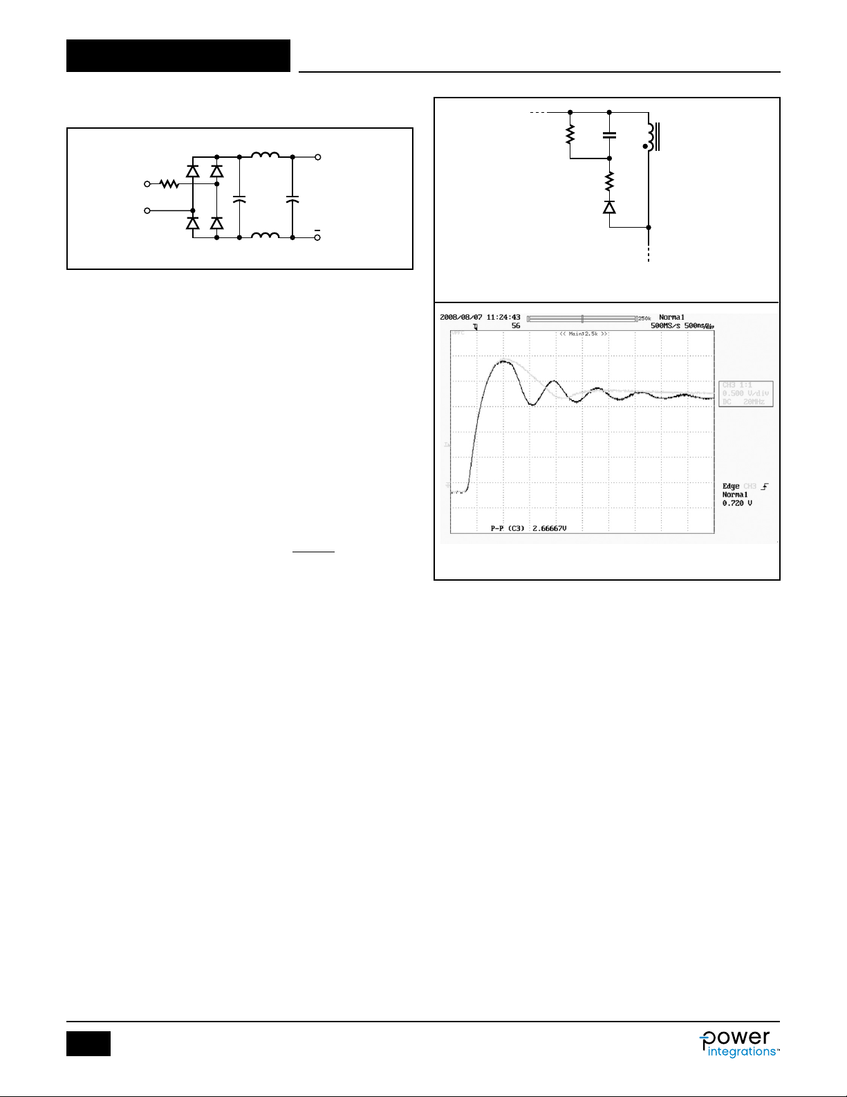
Primary Clamp Components
DC1: 1N4007 / FR107, 1 A, 1000 V
RC1: 100 W – 300 W
CC1: 220 pF – 1000 pF 500 V
RC1: 330 KW - 680 KW
The clamp arrangement, shown in Figure 25, is suitable for LinkSwitch-4
designs. Minimize the value of CC1 and maximize RC2 while maintain-
ing the peak Collector voltage to <(V
× derating factor). Larger
CBO
R
C1
D
C1
C
C1
PI-5107-012615
R
C2
Black Trace: DC1 is a FR107 (fast type, trr = 500 ns)
Gray Trace: D
Figure 25. Primary Clamp Components and Effect of Diode Recovery Time of
FEEDBACK Pin Voltage.
is a 1N4007G (standard recovery, trr = 2 us)
C1
values of CC1 may cause higher output ripple voltages due to the
longer settling time of the clamp voltage impacting the sampled
voltage on the feedback winding, particularly at low loads. A value of
470 KW for RC2 with 470 pF for CC1 and 100 W for RC1 is a recommend-
ed starting point for the RCD design. Verify that the peak collector
voltage is less than (V
conditions including start-up.
× derating factor) under all line and load
CBO
The clamp diode choice is governed by what weight is given to
various performance factors and cost. Customers usually favor
lowest cost at the power level and application type covered by
LinkSwitch-4 devices. This indicates the use of a low-cost 1N4007
slow recovery type diode. Note from Figure 25, that a slow recovery
diode has a lower frequency ring, and faster settling time, this can be
useful in reducing EMI.
The choice of snubber components affects no-load power, no-load
frequency, no-load output voltage stability, peak collector voltage,
efciency and EMI.
Reducing CC1 will reduce energy lost in the clamp, reduce the no-load
switching frequency and hence reduce the no-load power. The
compromise is that the peak collector voltage is increased and EMI
emissions may increase, but as long they are within the set limits it is
an option to control no-load power.
18
Rev. B 10/17
www.power.com
Page 19

Application NoteAN-69
Supplementary Base Drive
Resistor R
drive in higher power applications (7.5 W – 18 W) without increasing
is used on SO-8 packaged devices to provide extra base
SBD
package dissipation.
It should have a value of between 220 W and 390 W for standard
designs, or 100 W to 150 W for applications using the EasyStart
feature. Refer to ‘Step 15 – First Time Start-up and Troubleshooting’
to check that correct value has been selected.
Output Diode Snubber
It is advisable to allow for a output diode snubber in the application
design. It may not be required, but will aid EMC development if there
are places allocated on the PCB for these components. The snubber
consists of a resistor in series with a capacitor and are then placed in
parallel with the output diode. The snubber dissipates energy during
operation and reduces efciency, so it is advisable to only provide as
much snubbing as is required to pass EMC requirements. A 10 W
resistor in series with a 1 nF ceramic capacitor is a good starting
point. As a guide, the capacitor voltage rating should be equal or
greater than the output diode voltage rating.
Current Sense Resistor R
The value of RCS [E74] may need some adjustment to obtain the
CS
desired maximum output current i.e. the position of the constant
current region of the VI curve. This is due to the effects of the bias
winding, primary clamp and core losses drawing energy that would
otherwise go to the secondary. There is a nominal correction factor
in the calculations, but the amount of correction required varies with
power level and transformer design. Once the value has been
adjusted to give the desired current level, it will not change much
across production of the particular design. Some effort will have to
be made in centralizing the design so it remains within specication
across production, due to component tolerances, if required.
V
Setting Resistor R
CS(MIN)
LNK4xx2S parts do not need this resistor to set V
resistor should be included to enhance ESD immunity.
Voltage Feedback Resistor R
If R
is to be SMT then it should be at least 0805 size, preferably
FB1
two in series. During ESD events, a large voltage can be present
CS2
FB1
, but a 1 kW
CS(MIN)
across this resistor and it can be damaged.
Step 14 - Transformer Topology
The starting point for transformer design is not always the same
because it depends on constraints such as operating frequency and
transformer size. The transformer interacts with nearly all other
design considerations so it is impossible to design the transformer in
isolation. These interactions need constant consideration and review,
and the transformer design needs to be iterated to accommodate an
acceptable compromise throughout the design of the power supply.
For best efciency, use a core with as high a cross section area as
affordable. Also ensure that the winding window width is enough to
accommodate the secondary winding. The aim is a single layer of
secondary that fully lls the winding width; a 12 V design will there-
fore need a wider width than a 5 V design at the same power level.
Common LinkSwitch-4 Transformer Topologies
A simple 3 winding transformer structure has been developed that is
suitable for all LinkSwitch-4 designs up to 18 W. It may be necessary
to use a more complicated sandwiched secondary type structure with
5 windings, including a foil screen, at 7.5 W or greater to minimize
primary to secondary leakage inductance to optimize converter
performance. However, in a specic application a 5 winding structure
is not guaranteed to be superior to a 3 winding design. For cost and
manufacturing simplicity, it is recommended that a 3 winding
transformer is tried rst.
EMI conducted emissions are optimized by altering the number of
turns on the compensation winding. The number of turns on the bias
winding remains unchanged as it is designed to power the LinkSwitch-4
controller. It is the imbalance of the bias and compensation winding
turns, which are wound in the opposite sense, which provides the
compensation effect. The best balance is usually found within ±2
turns. Fractional turns can be used on the compensation wind for
optimal balance.
BJTs have slower switching edges than power MOSFETs, hence a
screen winding between the primary and the core is not usually
required. It tends to add signicant capacitance to the collector node
which degrades efciency and no-load power.
Wire size should be chosen such that each layer completely lls the
bobbin winding width. This can be compromised a little when a turn
or two is added or subtracted from the compensation winding, to
obtain the best EMI emissions performance.
Z-winding the primary, where each layer end is bought back to the
start side before winding the next layer, reduces the effect of inter
layer capacitance and signicantly reduces the no-load power.
Do not use unnecessary layers of tape as this will increase leakage
inductance and reduce efciency.
Simple 3 Winding Transformer
The 3 winding transformer is wound as the primary rst, with the
collector node pin as the start so that it is screened by succeeding
primary layers from the secondary.
The second winding is a combined bias winding and compensation
winding wound as a trilar (3 strand) winding. It is arranged that the
bias and compensation wind senses are in the opposite direction. On
average this tends to make the trilar winding have no net electrostatic voltage change, so it acts like a foil screen, though an imper-
fect one. Two strands are used for the bias wind and a single strand
for the compensation wind. It is possible to swap this to help obtain
a better compensation balance, or reduce VCC at maximum load if it is
too high.
The third winding is the secondary, wound in triple insulated wire.
A contact to the core material is made with tinned copper wire and
taken to +HT.
www.power.com
19
Rev. B 10/17
Page 20

Application Note AN-69
Figure 26. 3 Winding Transformer Construction.
5 Winding Transformer
The 5 winding transformer is wound as the primary rst, with the
collector node pin as the start so that it is screened by succeeding
primary layers from the secondary.
The second wind is a complete turn of copper foil that has the same
width as the bobbin winding window width. Care must be taken to
ensure the ends of the foil are insulated with tape so as not to form a
shorted turn. This is connected to the Bias wind GROUND pin.
The third winding is the secondary, wound in triple insulated wire.
The fourth winding is a combined bias winding and compensation
winding wound as a trilar (3 strand) winding. It is arranged that the
bias and compensation wind senses are in the opposite direction.
On average this tends to make the trilar winding have no net
electrostatic voltage change, so it acts like a foil screen, though an
imperfect one. Two strands are used for the bias wind and a single
strand for the compensation wind. It is acceptable to swap this to
help obtain a better compensation balance, or reduce VCC at maximum load if it is too high.
The fth winding is the remaining turns of the primary.
A contact to the core material is made with tinned copper wire and
taken to +HT.
Figure 27. 5 Winding Transformer Construction.
20
Rev. B 10/17
www.power.com
Page 21
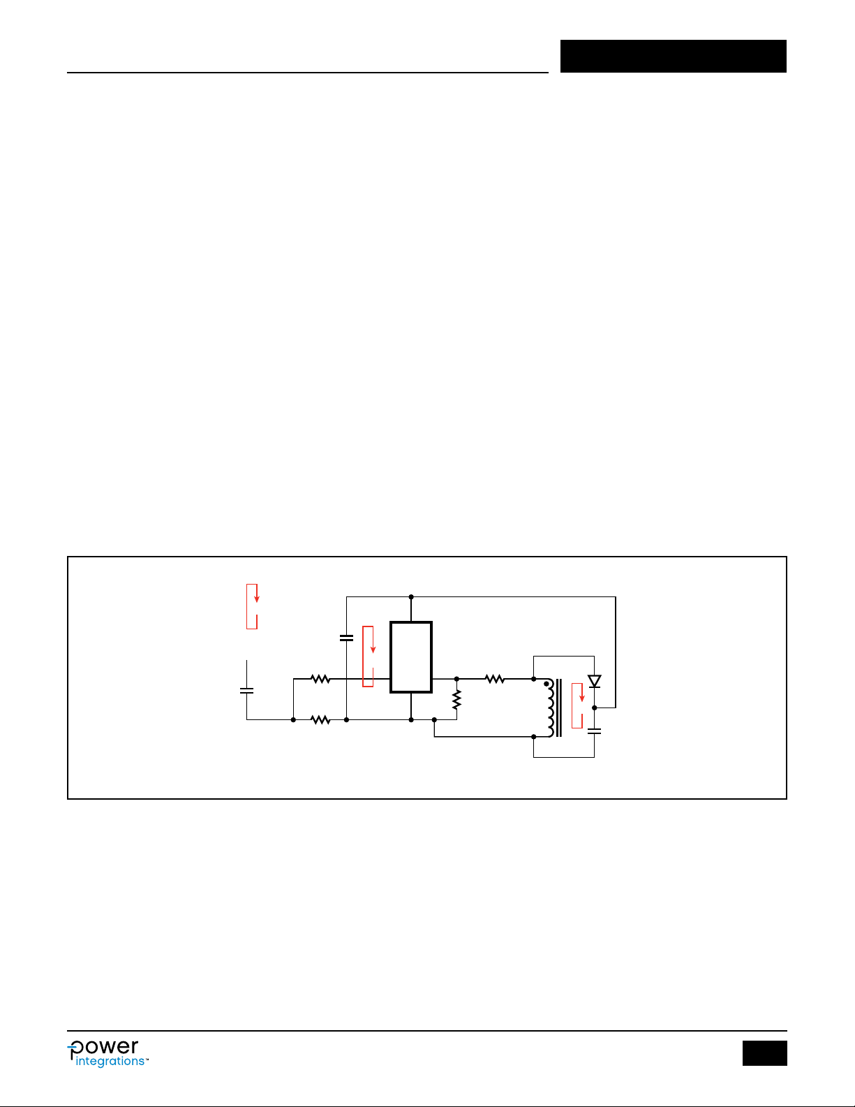
Application NoteAN-69
Step 14 – PCB Layout Guidelines
Good layout practice helps with:
• Achieving low EMI
• Good ESD immunity
• Thermal optimization
• Design for manufacture
Some simple, good practices and guidelines for routing are:
• Make track widths appropriate for current to be carried
• Space tracks according to voltage difference between them
• Keep tracks as short as possible.
• Prioritize critical paths: highest rst (high current, high frequency,
high-voltage)
• Keep thin tracks away from board edge
• Route tracks to center of a connecting pad
Functional Considerations
Loops (signal paths and ground returns) that carry fast edges are a
potential source of radiated EMI. The faster and larger the current
uctuations, the higher the radiated EMI power will be. Also the
larger the area enclosed by the loop, the higher the level of EMI. The
latter is where good PCB design can help, and poor design can cause
a real problem. The key is to keep current loops small and run out/
return tracks close together. Doing so keeps the loop area and
radiated emissions down.
Critical Connections
• The track between the feedback resistor R
GROUND pins must be as short as possible to avoid poor performance. C
recharge currents and primary current out of the
VCC
and LinkSwitch-4
FB2
GROUND pin must not generate volt drops in the GND tracking
that interfere with voltage on the FEEDBACK pin due to the GND
connection of R
• The impedance driving the FEEDBACK pin is quite high. As a
.
FB2
result, the FEEDBACK pin waveform can easily be distorted by
parasitic capacitive coupling from the primary BJT switch. When
laying out the PCB, it is important to minimize stray capacitance
between the switch and feedback node. This can be achieved by
placing the R
making the FB node small in area.
• The tracks between the BJT base and emitter to the BD and ED
FB1
and R
resistors adjacent to the FEEDBACK pin,
FB2
pins of the IC must be as short as possible to avoid poor EMI
performance.
• The tracks between the transformer and BJT collector must be as
short as possible and the total area as small as possible. If there
is a primary clamp circuit, the diode anode should connect to the
collector, not the resistor RC1, to minimize the high dv/dt node area.
• The current sense resistor R
the required rated current. The connections should be as small as
programs the power supply giving it
CS
possible and the track as wide as possible. The RCS resistance is
small and any track resistance will affect the operation of the
power supply. There should be dedicated tracks between R
both C
• Mount R
• Having a star point at the ground of the IC to all grounded
IN2
CS2
and R
. Highlighted nodes in Figure 29.
CS2
very close to the CS pin of the IC.
CS
and
components will help EMC and circuit performance, see Figure 28.
Note that the bias wind, D
loop, then its GND is connected to the star point.
BIAS
and C
form their own close small
VCC2
C
Figure 28. Star Point Ground Connections.
High current loops
– minimize area to
reduce radiated
emissions
c
VCC1
R
CS2
IN
R
CS
VCC
GND
R
FBCS
FB1
R
FB2
D
BIAS
C
VCC2
PI-8182-111016
www.power.com
21
Rev. B 10/17
Page 22
Application Note AN-69
R
RF1
C
L
IN1
1-4
D
IN
++
C
IN1
C
IN2
LinkSwitch-4
L
IN2
R
R
C2
CS
CS
GND
GND
CS
C
R
HT
BD
ED
VCC
FB
FB
VCC1
C
C1
R
C1
D
C1
T1
R
C2
Q1
C
VCC2
SSNUB
SSNUB
C
R
OUT
OUTVOUT
BS1
D
BIAS
+
R
BS1
PI-8164d-110116
D
OUT
C
R
FB1
R
FB2
+
Figure 29. Chip GND, RCS, R
D
, C
Connections.
CS2
IN2
L
IN1
1-4
IN
++
C
IN1
C
IN2
LinkSwitch-4
RF1
L
IN2
R
R
C2
CS
CS
GND
CS
GND
Figure 30. Primary Current Loop.
• The primary current loop (highlighted in Figure 30) must be kept
as small as possible because it has a moderate amplitude and fast
edges so needs low impedance (short, wide) paths. Keeping the
enclosed area as small as possible will help to reduce impedance
and EMI.
• The V
power rail needs to be tightly decoupled to reduce any EMI
CC
resulting from the switching action of the BJT and the recharging
of the VCC capacitors; highlighted in Figure 31. Two VCC capacitors
are usually required, each half the value given in [E138]. Keep
D
and C
BIAS
to form a very tight loop for the bias capacitor recharge current,
this signicantly helps radiated RF EMC. C
to the VCC and GROUND pins of the IC.
very close to the bias wind pins on the transformer
VCC2
must be very close
VCC1
R
R
BD
ED
VCC
FB
FB
C
HT
VCC1
C
C
C1
R
C1
D
C1
T1
R
C2
Q1
C
VCC2
SSNUB
SSNUB
C
R
OUT
OUTVOUT
BS1
D
BIAS
+
R
BS1
PI-8164a-110116
D
OUT
C
R
FB1
R
FB2
+
• One capacitor can be used, but this requires that the IC is also
next to the transformer bias wind pins and this can be difcult to
arrange.
• The output current path is where current from the output diode is
smoothed by an output electrolytic capacitor to make a DC output
and to reduce EMI. Due to high amplitude and fast switching
voltages and currents, it is important that the loop from transformer, diode and capacitor is made as small as possible. Keeping the
secondary snubber loop small will also help. The track area of the
secondary and output diode anode node must be kept small to
minimize capacitive coupling from the high dv/dt. If a through hole
output diode is used and mounted vertical to the PCB, place the
body anode end next to the PCB and the cathode end terminal
22
Rev. B 10/17
www.power.com
Page 23
1-4
D
IN
RF1
Figure 31. VCC and Bias Current Loops.
Application NoteAN-69
R
C
L
IN1
++
C
IN1
C
IN2
LinkSwitch-4
L
IN2
R
R
C2
CS
CS
GND
CS
GND
R
BD
ED
VCC
FB
FB
C
HT
VCC1
C
C1
R
C1
D
C1
T1
R
C2
Q1
C
VCC2
SSNUB
SSNUB
C
R
OUT
OUTVOUT
BS1
R
D
BIAS
+
BS1
PI-8164b-110116
D
OUT
C
R
FB1
R
FB2
+
L
IN1
DIN 1-4
R
GND
GND
BD
ED
VCC
FB
FB
C
HT
VCC1
RF1
++
C
IN1
C
IN2
LinkSwitch-4
L
IN2
R
R
C2
CS
CS
CS
Figure 32. Input Components and Tracks Susceptible to Noise from BJT Collector Node.
lead loop down to the output capacitor +VE track. Unfortunately
• A Y capacitor is effective at reducing EMI conducted emissions,
this is not optimal for good thermal cooling of the diode. The
cathode side track can be made large, as it only has a small ac
ripple voltage on it. It can act as a heat sink but the diode heat
has now to ow along the cathode lead before reaching the track.
Testing may be required to determine the best compromise. An
SMT diode would not have this problem.
• EMC will be reduced by ensuring a small loop area, for the primary
clamp circuit. Keep the components close to the transformer
primary pins.
• Noisy paths (shown in red in Figure 32) should be kept away from
the input loop (shown in green) to reduce capacitive coupling and
improve EMC. In particular, keep the BJT away from the input
diodes, L
and RIN. BJT collector node is the noisiest.
IN1
R
C
C
C1
R
C1
D
C1
T1
R
C2
Q1
C
VCC2
SSNUB
SSNUB
C
R
OUT
OUTVOUT
BS1
D
BIAS
+
R
BS1
PI-8164c-110116
D
OUT
C
R
FB1
R
FB2
+
particularly in the upper bands of 10 MHz plus. Power levels of 10 W
and above may benet from the use of a Y capacitor. However,
only low values should be used in wall adapters, about 470 pF
maximum, due to leakage currents presenting an unpleasant mild
shock risk. The Y capacitor should be connected from the +HT pin
of the transformer primary to the –VE of the secondary output as
shown in Figure 33. The Y capacitor provides a path for the high
frequency current through the transformer, capacitively coupled
from the primary to the secondary windings, to loop back to the
primary side, instead of owing down the output lead in a loop via
the EMI test equipment (LISN) and back up in a loop via the AC
input leads to the primary side. Currents owing through the
Y capacitor will not be measured by the LISN so the resulting
measurements will be lower.
www.power.com
23
Rev. B 10/17
Page 24
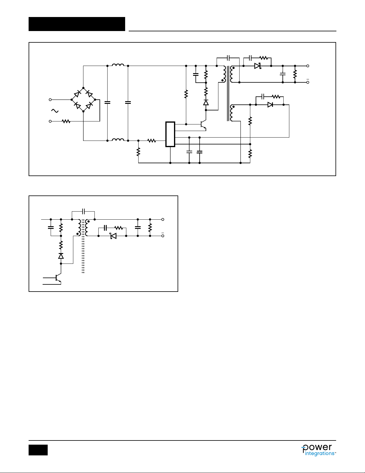
Application Note AN-69
L
IN1
1-4
D
IN
++
C
IN1
RF1
Figure 33. Y Capacitor Connection.
Y Capacitor
C
C1
R
C2
R
C1
D
C1
C
SSNUB
D
OUT
Q1
Figure 34. Alternative Y Capacitor Connection.
• Figure 34 shows an alternative Y capacitor connection and output
diode arrangement that may be more effective in some designs.
Thermal Considerations
Thermal management of enclosed power supplies is challenging.
PCBs are usually single-sided and do not have much copper to
conduct heat away from hot spots. In a sealed plastic enclosure,
there is little air circulation. Consider the following:
• Add printed copper (contrary to some EMC considerations).
• Keep hot components away from other components.
• Use 2 oz/in
2
copper.
• Use double sided boards.
The hottest components are likely to be the BJT and the output diode.
BJT Thermal Management
The LinkSwitch-4 drives the BJT in such a way as to greatly reduce
conduction and switching losses. However, thermal management is
still important. For good EMC, the BJT is required to be close to the
transformer and input capacitors, but these components also run
warm. Do not place the BJT body in contact with any other compo-
L
IN2
R
SSNUB
C
IN2
LinkSwitch-4
R
R
CS
C
OUTROUTVOUT
+
PI-8165-100217
C2
CS
CS
GND
GND
+
R
C
SSNUB
SSNUB
C
R
OUT
OUTVOUT
BS1
D
BIAS
+
R
BS1
PI-8164e-110116
D
OUT
C
R
FB1
R
FB2
+
R
BD
ED
VCC
FB
FB
C
HT
VCC1
Y Capacitor
C
C1
R
C2
R
C1
D
C1
Q1
C
VCC2
T1
nents. Although the collector node should be kept physically small to
reduce EMI, it is possible to use the connection to conduct heat away
from the BJT, to the transformer. Base and emitter connections may
be made wide to help conduct heat away from the BJT and into the
PCB substrate.
Arrange for a substantial amount of copper to the GND pins. These
pins conduct heat out of the chip, particularly on the SO8 packaged
parts which dissipate higher power.
Output Diode Thermal Management
The output diode dissipates signicant power. Consider the following
when placing the diode:
• The connection between transformer secondary and diode (usually
the anode) has a high frequency voltage on it so should be kept
small in order to reduce stray capacitance and radiated EMI.
• The transformer may act as a heat sink for the diode so keep the
connection short.
• Long leads on axial diodes increase the thermal resistance from
the die to the PCB. Laying the diode at reduces total lead length.
• The printed copper connected to the DC side of the diode (usually
the cathode) may be large without radiated EMI so may be used as
a heat sink.
ESD Considerations
PCB layout for ESD should ensure low impedance from the source of
the ESD transient on the output, to ground via the mains supply.
Transformer insulation should present higher impedance to the surge
than the spark gap. The spark gap must break down before the
transformer insulation does.
A spark gap does not divert all the energy of an ESD event away from
the control circuitry. The ESD strike is a low impedance, very high
dv/dt event, and the capacitance between the secondary, bias, screen
and primary windings will cause a high current to ow from the
secondary side to the primary side tracking, particularly from the
transformer GND and +HT pins. Also, when the spark gap breaks
down, the transformer capacitances are discharged, causing a high
current ow in the opposite direction. The circuitry will probably be
more susceptible to one direction than the other, so if the initial strike
has no effect, the spark gap breakdown may cause a failure.
24
Rev. B 10/17
www.power.com
Page 25
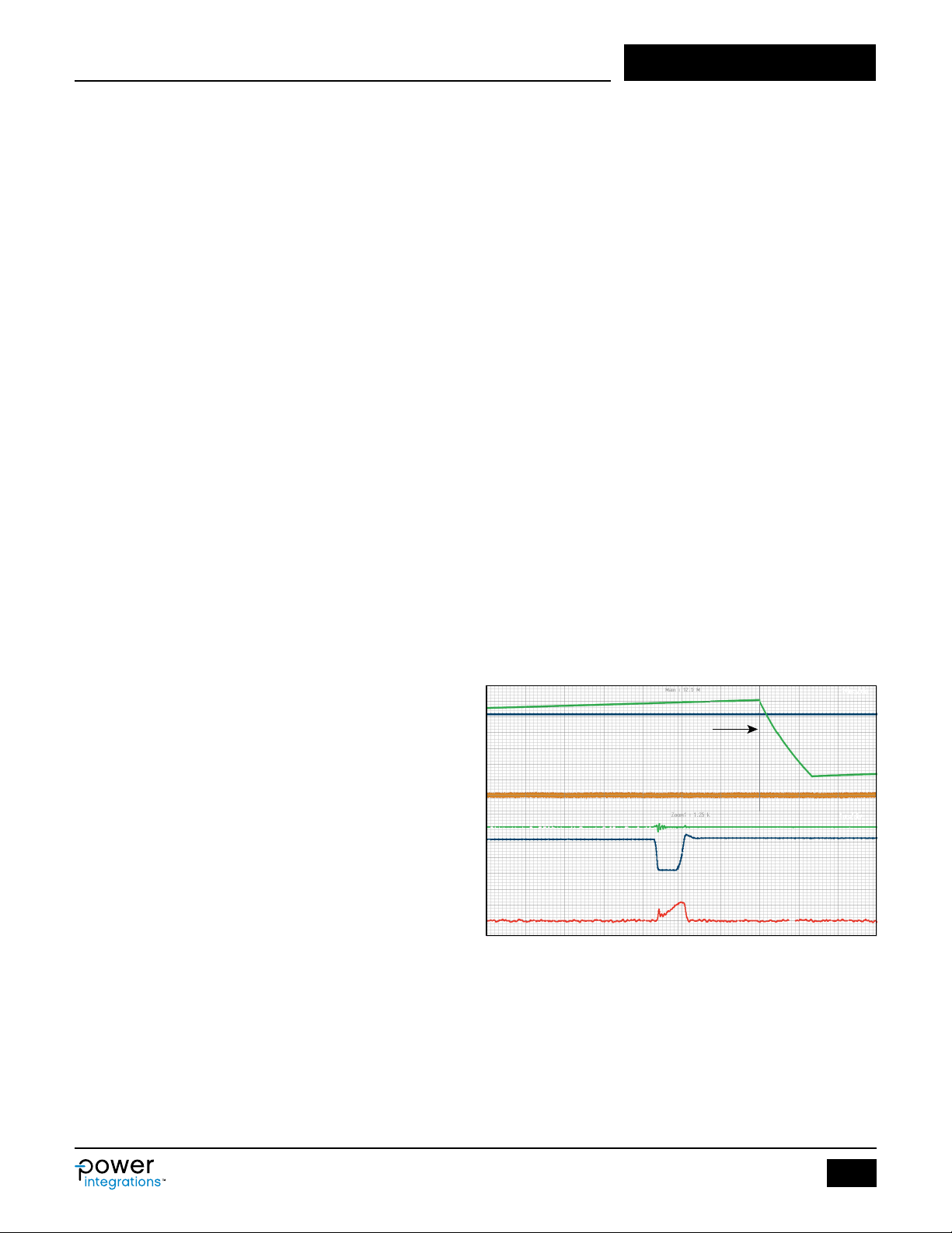
Application NoteAN-69
The PCB has to provide the lowest possible impedance to ground
through the spark gap.
• Distance between the spark gap points should be the minimum
and no more.
• Some customers can work with a 4.6 mm gap with a routed slot.
Check with the customer before designing the PCB. The standards
state 6.4 mm.
• The spark gap should have short, wide tracks from as close to the
output as possible, to as close to the mains terminations as possible.
• It should go to the AC side of the rectier bridge rather than the
DC side, and directly to the AC terminal, not through any input
surge limiting resistor.
• The primary-to-secondary creepage path, that is, the path over the
PCB surface, must be shortest through the spark gap.
• The greater the difference between the spark gap length and the
other primary to secondary creepage distances the better.
• Spark gap terminals should be pointed to minimize the spark
overvoltage.
• Be aware of discharge paths through air – from output caps to
core, for example. A common path is from the secondary
terminals to the core, which is usually connected to the +HT which
may not be a problem, but it may be connected to the chip GND
for EMI purposes; this would probably lead to a failure.
• Cut the leads of through-hole components ush with the solder
llet so there are no sharp points to encourage sparking along an
undesirable path.
• Input lter inductors L
spark gaps in parallel with them, to prevent inductor damage
IN1
and L
should have single point short
IN2
during an ESD event, especially if a Y capacitor is used. This spark
gap can be the minimum gap allowed by the PCB layout rules, say
0.25 mm. Each side of the gap should be a single point so a
minimum of additional capacitance is added across the inductor
which could reduce its ltering effectiveness.
• As a large current may pass along the chip GND tracking, it is
important that the GND tracking layout guidance is followed.
• Always include R
protection to the primary CURRENT SENSE pin from ESD events.
• Include a low value resistor in series with D
greatly enhances ESD immunity. It does have a side effect of
in LNK4xx2S designs at 1 kW. It affords some
CS2
of 1.2 W. This
BIAS
causing a slight uplift in no-load output voltage of about 50 mV/W,
the higher the resistance the greater the uplift.
• Some customers require ESD immunity up to 20 kV+, this can be
challenging. An additional capacitor, 100 pF / 220 pF between the
BASE DRIVE and EMITTER DRIVE pins, can provide extra
immunity. The chip may be glitched into the restart cycle, but
should not fail catastrophically at the higher test voltages.
Step 15 – First Time Start-up and
Troubleshooting
Safety
Ofine power supplies, particularly in a development situation, can
exhibit hazards including but not limited to electric shock, high
temperatures, re and smoke. They should be operated and used
only by competent, trained personnel. In particular:
• The unit to be tested should be checked for design and build errors
before applying mains power;
• The unit under test should be powered via a suitable isolating
transformer and a variac;
• Hazardous voltages are present in both normal and abnormal
operating conditions;
• Insulation between high-voltage and low voltage parts may not
provide safety isolation;
• All connections should be regarded as LIVE and HAZARDOUS;
• Before modifying the circuit or applying a soldering iron to add/
remove components, it is essential to discharge the bulk capacitors
completely. Also the C
charged. Damage can occur to the chip if there is charge on the
C
capacitors and a soldering iron is applied to the chip pins or
VCC
associated components. This is in addition to the usual shock
capacitors must be completely dis-
VCC
hazard presented by residual charge on capacitors.
Attach test points and connect oscilloscope probes to:
1. Collector node, use HV x100 probe 50 V / div. DC, GND clip to
chip GND node;
2. VCC node, 5 V / div. DC, GND clip to chip GND node;
3. –HT/RCS node, 20 mV / div. DC inverted for clarity, GND clip to
chip GND node. This should be a small loop area RF type
connection across RCS to acquire accurate waveforms.
Monitor AC input with DMM or metered AC source and monitor output
with DMM or electronic load.
Set to zero AC voltage input and no-load. Set scope to auto run and
10 ms/div time base.
Assuming a standard design;
Turn on AC source and increase to about 40 VAC.
Collector node should increase to √2 x AC input.
VCC should ramp up to V
then ramp up again and repeat. The output remains at zero volts.
, then quickly discharge back to V
CC(RUN)
CC(SLEEP)
If the VCC remains low, ~0.7 V, then check the chip is mounted
correctly. Measure the EMITTER DRIVE pin voltage, if it is ~0.7 V
above the VCC level, then the chip has been damaged and must be
replaced.
Switch scope to Normal sweep and trigger from the VCC node channel,
-ve edge and set level to trigger just below V
VCC just starts to fall and locate the collector and V
. Zoom in to where
CC(RUN)
pulses.
RCS
Captured waveforms should look similar to Figure 35.
10ms/div
Zoom Area
1us/div
Magnied Waveforms
Figure 35. Start-Up Waveforms Where VIN is Below UVLO Level.
CH1 = Collector Node, CH2 = V
, CH3 = VCC.
RCS
Sequence of events;
1. VCC rises to V
2. LinkSwitch-4 wakes up, initializes and draws a higher current
I
and C
VCC(RUN)
3. Once initialized, a single pules is issued (Probe Pulse). This
, ~13.5 V;
CC(RUN)
starts to discharge.
VCC
measures the voltage level of +HT via primary/bias winding
turns ratio plus the value of resistor R
4. As AC/HT level is below UVLO, the probe pulse terminates after
;
FB1
about 600 ns;
,
PI-8238-011617
www.power.com
25
Rev. B 10/17
Page 26
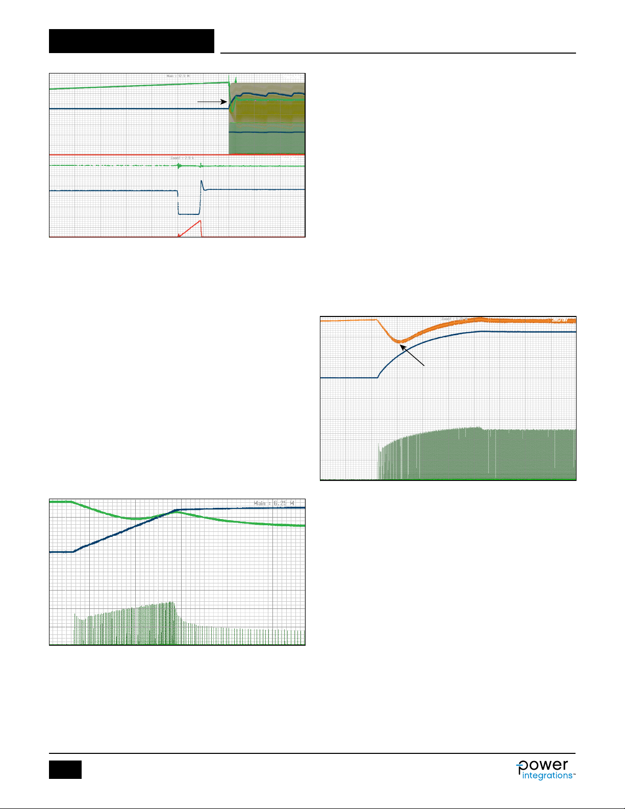
Application Note AN-69
10ms/div
Zoom Area
2us/div
Magnied Waveforms
Figure 36. Start-Up Waveforms Where VIN is Above UVLO Level.
CH1 = Collector node, CH2 = V
5. No more pulses are issued and VCC discharges to V
6. LinkSwitch-4 goes to sleep and VCC rises again and the cycle
, CH3 = VCC.
RCS
, ~4.5 V;
CC(SLEEP)
repeats.
Increase the AC supply to ~90 VAC, the circuit should run continu-
ously and the output voltage should rise to the designed level.
To compare the probe pulse when VIN/HT are above UVLO level, turn
off the AC source, discharge the bulk and VCC capacitors and set the
scope to single shot. Turn on the AC source and the scope will
trigger near the probe pulse. The resulting waveforms should look
similar to Figure 36.
Notice that the BJT ON-time has increased to ~1.8 ms and V
reaches the V
LNK40X2S parts. It is the V
pulse when the UVLO level is exceeded. This time, after the probe
level set by R
CS(MIN)
, or the single level set by the
CS2
threshold that terminates the probe
CS(MIN)
RCS
pulse, the circuit continues switching at the maximum rate until the
output voltage reaches it design level. The LinkSwitch-4 draws power
from C
voltage to charge the capacitance and power the chip as can been
capacitance until the bias winding generates enough
VCC
seen in Figure 37 and Figure 38.
Care must be taken to ensure VCC does not rise above 16 V, else the
chip may be damaged.
The bias winding voltage is related to the output voltage by the
secondary/bias turns ratio. Initially the output voltage is zero due to
PI-8239-011617
the zero charge on the output capacitance and it takes time for the
output voltage to rise to a level where enough voltage is generated
by the bias winding to power the chip. When starting into no-load, all
the generated output current, ICC, charges the output capacitance, so
the output voltage rises quickly, so the bias winding soon reaches a
level where it can power the chip. During this time the voltage on
C
will only fall by about 5 V.
VCC
Start-up when fully loaded, particularly into a CC load, charging the
output capacitance takes much longer as the available current to
charge the output capacitance is now only ICC – I
to fall much lower before the bias winding can supply power, see
Figure 38. If VCC is allowed to fall to V
switching and the start-up process will begin again and the circuit
CC(SLEEP)
. This allows V
LOAD
, the chip will cease
may never fully start-up. To avoid this check that VCC does not fall
below 6 V during start-up, or at least 5.5 V as an absolute minimum
but with reduced production tolerance.
Starting into a highly capacitive load also runs the same risk.
V
CC
2ms/div
Recommended VCC Minimum
During Start-Up of 6 V
V
OUT
V
/Primary Current
RCS
Figure 38. Start-up into Full Load.
CC
PI-8241-011617
500 us/div
V
CC
V
O
5 V/div
5 V/div
Zoom Area
Zero Load
Figure 37. No-Load Start-Up Detail.
The VCC voltage is designed to be 8 V – 9 V at no-load, but when
supplying current to the output when under load or during start-up,
when the output capacitance is being charged, the higher primary
current stores more energy in the leakage inductance. This is
harvested by the bias winding, which is more closely coupled to the
primary, and causes VCC to rise above the no-load level.
26
Rev. B 10/17
If start-up problems are encountered:
1. Reduce the output capacitance. Retaining the can size increases
the rated voltage and maintains the ESR and current rating of an
PI-8240-011617
electrolytic capacitor. If there is a no-load transient specication,
reduce V
2. Increase the value of maximum current ICC for the design to
to compensate i.e. increase no-load frequency.
CS(MIN)
charge the output faster.
3. Increase the value of C
4. Use a LNK40x4D, with the EasyStart feature.
, but do not exceed 2.2 mF.
VCC
No-Load Power
A target of 30 mW no-load power is usually easily achievable using
the component values suggested by the design tool and a ‘Z’ wound
primary.
Optimization may be required where there is insufcient margin or
meeting USB dynamic transient response has increased the no-load
power level.
www.power.com
Page 27
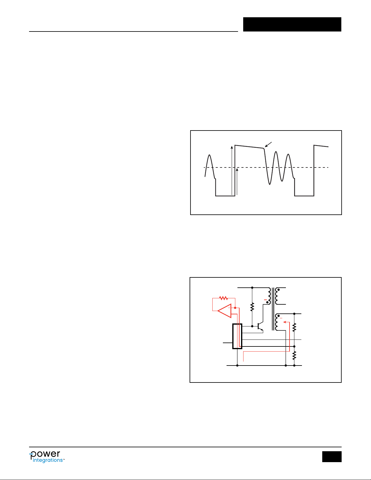
Application NoteAN-69
To improve no-load power, the following steps can be taken;
1. Start-up resistor can be increased. 30 MW is a value that is
usually used to provide a fast sub 1 second start-up, but 40 MW
should just be OK across production spreads for a universal input
application. Above 40 MW BASE DRIVE pin leakage at higher
temperatures can cause problems.
2. The primary clamp/snubber components can be made less lossy.
Reducing the value of the capacitor can be helpful if using a slow
clamp diode (1N4007). This will reduce the no-load frequency.
3. Increase the value of the dummy load resistor. Ideally, the power
dissipated by the dummy load should be equal to the power
dissipated by the IC. This helps to control the no-load output
voltage to the desired level across production variations.
Leakage inductance might allow a 25 or 50% increase in dummy
load resistance without incurring no-load output voltage drift,
usually upward.
(2) & (3) will result in the no-load frequency reducing, which is good
for no-load power as switching losses which are dominant at 230 VAC,
but this may compromise USB transient response performance.
On LNK40x3/4 devices, no-load frequency and USB transient response
performance can be restored by selecting a lower level of V
No-load frequency will increase again, but the energy per cycle has
CS(MIN)
.
been reduced.
Thorough pre-production testing would be required to check the
suitability of these changes as they depart from the safe recommended
design values.
SBD Resistor Check
Referring to Figure 46, for a standard design, if the value of the SBD
resistor is correct, then the time period t3 – t4 should be visible when
monitoring the BASE DRIVE pin voltage. It will appear as a slight
step down towards the end of the base drive period and should be
present from 90 VAC to 240 VAC on a universal input design. Beyond
240 VAC, the period may reduce to zero, this is OK and not critical.
Referring to Figure 50, for designs using EasyStart, t3 – t4 must be
visible up to 264 VAC in order for EasyStart to function at all input
voltages and aid starting.
Initial Basic Design Check List
• Check design specication points met i.e. VI curve, no-load power,
efciency, start-up time.
• Check component temperatures at maximum load and at maximum
and minimum input voltages.
• At maximum load I
V
.
CS(MA X)
• Check R
start-up at maximum and minimum input voltages for signs of
voltage waveform at maximum power, load transient and
CS
, peak CS voltage should be about 70-85% of
CC
transformer saturation.
• Check peak collector voltage at maximum load, transient load and
start-up at maximum input voltage.
• Check output and bias diode maximum reverse voltage stress.
• Check short-circuit output current at maximum input voltage with
RCS shorted and un-shorted.
• Check no-load output voltage at maximum input voltage with R
shorted.
• At no-load, the peak of the AUX voltage must be greater than 6.5 V.
• Check AUX voltage at maximum output power and maximum input
CS
voltage.
• What is the ESD voltage at which the spark gap ashes over with
the transformer removed from the circuit? Does the PCB ash over
at points other than the spark gap?
• What is the ESD voltage at which the transformer ashes over
between primary and secondary, when it is tested out of the circuit
with primary pins shorted and secondary pins shorted? Is this
greater than the PCB spark gap ESD breakdown voltage?
LinkSwitch-4 Functional Description
FEEDBACK Pin
The transformer voltage is monitored by dividing the bias (feedback)
winding voltage and feeding the signal into the FB node. The signal
contains all the information necessary for voltage regulation, current
regulation, valley switching and protection of the BJT:
1. Input voltage (VHT).
2. Collector voltage.
3. Idle ring voltage peaks and valleys.
4. Output voltage before the output diode.
5. Charge time (primary conduction).
6. Discharge time (secondary conduction).
4- Output voltage sampled here
6
2
0
1
5
Figure 39. Bias Winding Feedback Waveform.
When bias winding voltage goes negative, an active internal circuit
provides the current required to hold the FEEDBACK pin at zero volts.
Current sourced from FEEDBACK pin matches current in upper
feedback resistor R
Current sourced from FEEDBACK pin is internally translated to a
. Current in lower feedback resistor R
FB1
positive voltage that represents a scaled bulk voltage.
+
BD
ED
VCC
CS
FB
GND
Figure 40. Internal Virtual Ground Amp Holds FEEDBACK Pin at Zero Volts for
-V
Input.
E
ON
I
3
3
PI-8162-103116
is zero.
FB2
+
+
FB
PI-8163-110116
www.power.com
27
Rev. B 10/17
Page 28

Application Note AN-69
/VRINN
HTLO FB FBHT LO PB1
##=
^h
/VRINN2
INSTARTFBFBHTSTART PB1
## #=
^h
R
RR
N
N
FB
B
2
##
+
The controller measures the FB source current to determine the
voltage across the primary, and applies two thresholds, I
I
I
to sustain normal operation, or it may indicate that the FEEDBACK pin
.
FBH T(START)
is the threshold at which the primary voltage might be too low
FBH T(LO)
FBH T(LO)
and
is not connected to the feedback winding due to a fault. When
detected, drive to the primary switch is disabled so VCC decreases.
When VCC falls to V
cycle but this is negated by the low mains condition. Therefore, the
voltage continues to fall to V
and a restart cycle is initiated.
I
the HT voltage level is high enough to sustain the start-up cycle
is used by the rst pulse, the probe pulse, to establish that
FBH T(START)
, the controller requests a new switching
CC(LOW)
and the controller goes to sleep
CC(SLEEP)
safely and give a smooth monotonic output voltage rise.
FEEDBACK
pin current
Figure 41. Feedback Winding Voltage Waveform and Current into FEEDBACK
Pin During -V
Resulting FEEDBACK
pin voltage
FEEDBACK pin -V
not held at zero by FEEDBACK pin
Input.
E
voltage if
E
PI-8161-012517
The actual voltage levels these thresholds equate to on the primary
are controlled by the primary / bias turns ratio and the value of R
.
FB1
i.e. For the HT brown-out voltage;
Too little
slope
OV
VAUX
Figure 43. Slope Detection of Knee Point.
Tangent
Optimal
Knee
point
Flyback Switch-On
Too much
slope
PI-8243-012417
FEEDBACK Pin, Measuring the Output Voltage
To obtain an accurate measure of the output voltage, the feedback
waveform is sampled at the end of the secondary discharge period,
Figure 42, when the secondary current has fallen to near zero. This
avoids inaccuracies due to resistive volt drops associated with the
resistances of the output diode, secondary wire, tracking and output
capacitor ESR.
A slope detector is used to detect this point, the ‘knee point’; the
feedback waveform is sampled whenever the dv/dt of the input signal
is equal to the slope detector value.
A sample is taken each time the slope detector triggers, even on the
leakage inductance ringing, each sample overwriting the preceding
sample. The last sample taken before the feedback waveform passes
through 0 V (FEEDBACK pin voltage to current transition) is the value
used in determining the output voltage at that time.
To ensure the correct zero crossing point is used, there is a blanking
time, t
may pass through zero and cause a false nal sample detection.
Under no-load conditions, it is essential that the secondary discharge
time exceeds t
Figure 43. The design software checks for this.
Different values of t
chosen and whether signicantly in constant current mode or not.
, to mask off the leakage inductance ringing, where a ring
FBBL
, so that the true zero crossing point is not blanked,
FBBL
are set depending on the level of V
FBBL
CS(MIN)
To calculate the AC input start voltage;
V
FBHT(IO)
V
FBHT(START)
Figure 42. Feedback Winding Reference Points as Voltages.
28
Rev. B 10/17
t
DCHARGE
t
FBBL
0 V
Without blanking, FB
0 V
Figure 44. FEEDBACK Pin Blanking Time t
crossing 0 V would cause
false knee point detection
.
FBBL
PI-8159-103116
The output voltage is determined by the formula;
FB FB
12
PI-8160-103116
VV
=
OUTCVFBREG
As R
is used to set the brown-out and start-up voltages, R
FB1
used to set the output voltage.
^h
S
is
FB2
www.power.com
Page 29

Application NoteAN-69
RV
N
S
#
The voltage control loop aims to maintain the sampled value at
V
, about 1.98 V, see data sheet.
FB(REG)
(()
1
V
OUT(CV)
FB FB REG
N
B
#=-
to ne tune the output voltage.
FB1
V
FB REG
)
or
FB1
R
2
FB
Small changes can be made to R
If no signal is present on the FEEDBACK pin i.e. open circuit R
short-circuit R
circuit will continuously run the start-up cycle (hiccup) due to the lack
or open circuit tracking, switching will cease and the
FB2
of signal.
Quasi-Resonant Switching
The primary switch is only turned on when the voltage across it rings
down to a minimum (voltage-valley, quasi-resonant switching). This
reduces EMI and switch turn-on loss. Again, a slope detector is used
to sense the idle ring valleys in the FEEDBACK pin signal. If the idle
ring has decayed and is undetectable, the next switching cycle will
start without waiting for a valley detection.
Cable Compensation
Cable compensation is xed per variant. The controller alters the
voltage control signal produced during the comparison of VFB and
V
, thus making the necessary adjustment to compensate for the
FB(REG)
output voltage drop across the cable. The set value of cable
compensation is accurate at the top right of the VI output curve i.e.
the CC current setting, not necessarily the label current rating, which
is usually lower.
VOLTAGE SUPPLY Pin
The VCC pin supplies power to the internal circuitry. There is an ultra
low power series regulator supplying logic and analogue circuitry.
Constant current sources that drive the BJT are sourced directly from
the VCC pin. Being an ultra low power regulator results in it being
not very fast, so it is important that the VCC pin is very closely
decoupled to the GROUND pin via C
The VCC pin has several thresholds that prompt specic actions form
the controller.
1. V
and enter sleep mode and the current drawn through the
; If VCC is below V
VCC(SLEEP)
VOLTAGE SUPPLY pin falls to a few mA (I
2. V
3. V
; If in sleep mode and VCC rises to V
VCC(RUN)
initializes and the VOLTAGE SUPPLY pin current increases to
I
and a probe pulse is issued (see Start-up sequence
VCC(RUN)
section and Step 15, First time start- up).
; If the controller is in Run mode and the VCC voltage falls
VCC(LOW)
to V
as it does not overlap a pulse already issued. This function is
, an extra switching pulse is issued immediately as long
VCC(LOW)
useful when there is a high load to no-load transient. The output
voltage will overshoot a little and will cause a frequency lower
than the design no-load frequency to be set. The period of this
frequency may be so long that the VCC voltage falls lower than it
would during a stable no-load situation. To prevent the VCC
voltage falling to V
cycle sequence, an extra no-load type pulse is issued which adds
charge to C
will take a little longer to recover from the output voltage over-
and prevents a shutdown. The side effect is that it
VCC
and causing a shutdown and power
VCC(SLEEP)
shoot, but at least the switching operation is continuous and a
power cycle glitch is avoided.
4. ∆V
between the peak and minimum VCC voltage due to the charging
and discharging of C
operation, at least a 50 mV rise must be detected in the C
; During no-load operation, this is the difference
VCC(PFM)
during a switching cycle. During no-load
VCC
voltage to proceed to the next stage of the switching cycle,
.
VCC
the controller will stop switching
VCC(SLEEP)
).
VCC(SLEEP)
, the controller
VCC(RUN)
VCC
otherwise switching will cease, VCC will fall and a power cycle
sequence will occur. If VCC falls by 1.6 V, an extra switching pulse
is issued as if VCC had fallen to V
V
.
VCC(LOW)
, even if VCC is higher than
VCC(LOW)
CURRENT SENSE Pin
The CURRENT SENSE pin serves two functions;
1. During Initialize mode, during start-up, the value of R
by sourcing a constant current from the CURRENT SENSE pin and
measuring the resulting voltage with a 2 bit ADC. This results in
one of four possible values being detected, which sets the chosen
level of V
values of resistor and corresponding levels of V
in an internal register. See data sheet for available
CS(MIN)
LNK40X2S parts only have one xed level of V
perform this routine. However, R
value of 1 kW, as an ESD protective measure.
should still be present with a
CS2
2. The CURRENT SENSE pin measures the –VE voltage across the CS
resistor RCS, which is due to the volt drop across RCS caused by
the primary current.
This voltage is scaled internally and compared to the control
voltage and the over-current protection threshold (V
determine when the switching BJT should be turned off. Note
that if the over-current sense threshold is reached, there is a
small delay (t
propagation delay. This results in the observed OCP level being
) before the BJT is turner off due to internal
CS(O FF)
higher than the expected value and it is dependant upon the HT
voltage at that time. Conversely, when the voltage across RCS is
governed by the control voltage, the observed RCS voltage is
exactly as expected because the delays are compensated by the
control feedback loop. In normal regulation the maximum value
of voltage across RCS is limited to V
power limit during transients or running at low HT voltage. Note
. This acts as a maximum
CS(MA X)
that the transient power limit will usually be higher than the V
× ICC steady state circuit power limit.
There is a CURRENT SENSE pin leading edge blanking time of
t
, so charging of stray capacitance does not cause a false
CS(B)
triggering of BJT turn off.
If RCS resistor is open circuit then the primary current will ow
through the internal ESD protection diode between the GROUND pin
and the CURRENT SENSE pin, the voltage on the CURRENT SENSE
pin will very quickly reach the OCP or control voltage governed levels
and the switching BJT will be turned off. This will result in very little
energy in the primary, so at no-load, the output voltage may be
correct, but when a load is applied, the output voltage will fall.
If the RCS resistor is short-circuited or the connection to the CURRENT
SENSE pin is open circuit at start-up, the controller will not start. It
will issue the probe pulse and immediately go to SLEEP mode. It will
then attempt to re-start. It will hiccup. If there is no-load on the
output, the output capacitor will charge to a level dependent on the
value of bleed (dummy load) resistor and the hiccup rate. Because
the controller doesn’t wake up properly, the output overvoltage
protection will not be active.
The controller is able to detect if RCS is shorted or connection open
circuit during normal running. This is done by detecting switching
BJT desaturation on the FEEDBACK pin signal. If the condition
persists for a predetermined period, then the controller goes to
SLEEP mode. If the output voltage reaches the output overvoltage
threshold before the predetermined period expires, then the
controller goes to SLEEP mode.
It is difcult to predict the output voltage with RCS shorted so it must
be measured at no-load and maximum input voltage.
CS2
.
CS(MIN)
and does not
CS(MIN)
CS(O CP)
is measured
) to
OUT
www.power.com
29
Rev. B 10/17
Page 30

Application Note AN-69
R
CS
CS(CC)
I
N
V
^h
Constant Current Control by the CURRENT SENSE
Pin Average Voltage
The controller evaluates the average voltage across RCS. This is used
to control the maximum output current of the circuit. A current
control loop aims to limit the average voltage to V
limit, the voltage control loop is dominant, but at and beyond the
limit, the current control loop is dominant.
Averageprimary current
__
So by transformer primary to secondary turns ratio;
OUT(CC)
N
R
S
CS
CS CC
P
=
However, the VCC supply and primary clamp take energy out of the
transformer so an actual circuit will be a little lower than this
calculated value. It can be trimmed by RCS and once a design is xed,
this error remains fairly constant through production. So once
trimmed for a design, the maximum output current will remain
consistent across production.
EMITTER DRIVE Pin
Internally, the EMITTER DRIVE pin is connected to a pull down
MOSFET. This connects the switching BJT emitter to GND during the
‘Charge’ period of the switching cycle. This MOSFET must be capable
of conducting the peak primary current without incurring signicant
power loss. There is also a pair of ESD protection diodes, one from
GROUND Pin to the EMITTER DRIVE pin and a second from the
EMITTER DRIVE pin to the VOLTAGE SUPPLY pin. This second diode
is used during the start-up cycle to charge the capacitor C
passing the BJT’s emitter bootstrap current from the EMITTER DRIVE
to VOLTAGE SUPPLY pins.
The switching of this pin is synchronized with the BASE DRIVE pin to
enable rapid and safe, controlled switching of the BJT, see Figures 45
and Figure 46.
BASE DRIVE Pin
The BASE DRIVE pin supplies current through the switching BJT base
to turn it on quickly, but provide only just enough charge to keep the
BJT saturated whilst allowing it to be rapidly turned off. Like the
EMITTER DRIVE pin there is a pull down MOSFET , but this is used to
turn the BJT off. This too must be capable of conducting the peak
primary current as the primary current is passed through the BJT
base when the EMITTER DRIVE pin MOSFET is turned off. This
speeds up the turn off of the BJT.
There are four stages in the base drive cycle, see Figure 45 and
Figure 46;
1. A high initial level of base current for a short duration, the ‘Force
On Pulse’, amplitude I
2. A controlled level and duration of base drive based on the output
power demand. The level is proportional to the control voltage
and the duration is controlled by a feedback loop that aims to
keep the time between pulling the base low and the collector
rising by approximately 30 V to around 100 ns. Additional current
may be supplied by the SBD resistor via the SUPPLEMENTARY
BASE DRIVE pin, at this time for higher power designs using
SO-8 packaged devices.
3. A period where the BASE DRIVE pin is high impedance and the
BJT consumes the charge stored in the base region in order to
conduct the primary current.
4. BASE DRIVE pin is pulled low to turn the BJT off. The EMITTER
DRIVE pin simultaneously goes high impedance.
, duration t
F(ON )
F(ON )
.
V
=
. Before this
CS(C C)
VCC
by
V
CC
BD current
level control
Logic
BD
I
1
I
2
Logic
BD GND
Figure 45. Simplied Base Drive Circuit.
Logic
ED GND
BD
ED
b
I
BD
V
CC
I
ED
V
CE
V
ED
t1t
2
t
3
Logic
BD
Logic
BD GND
Logic
ED GND
Figure 46. BJT Switching Cycle Waveforms.
PI-8158-103116
a
t4t
5
ON
OFF
ON
OFF
ON
OFF
PI-8154-102816
30
Rev. B 10/17
www.power.com
Page 31
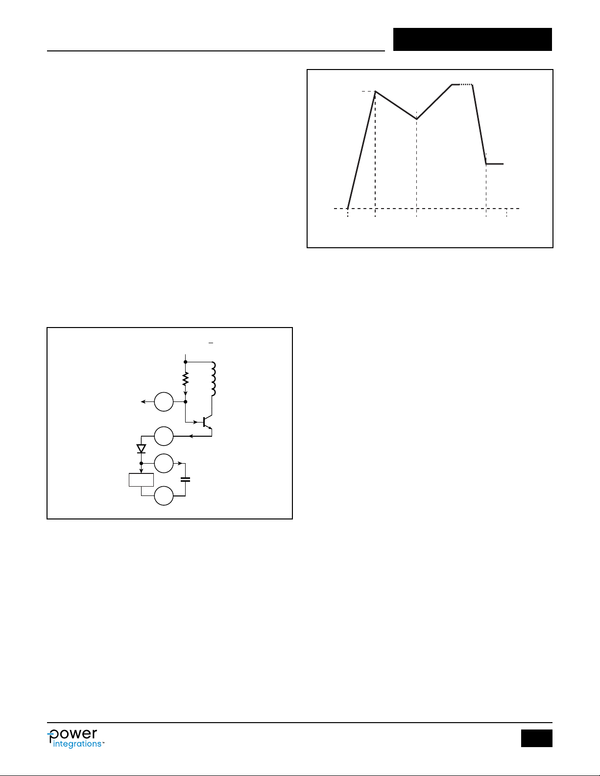
This scheme allows for a wide range of BJT HFE characteristics to be
driven efciently with minimum power loss. As the drive is essentially
‘common base’, the full RBSOA of the BJT can be used i.e. V
is dominant, not V
• (t1 – t2) Force ON pulse (“fon”).
• (t2 – t3) Variable adaptive base drive.
• (t3 – t4) BJT storage time.
• (t4) BASE DRIVE pin pulled to GND, emitter released.
• (t4 – t5) VCE rise time, BJT turning OFF.
CEO
.
CBO
rating
SUPPLEMENTARY BASE DRIVE Pin
LinkSwitch-4 parts in a SO-8 package have a SUPPLEMENTARY BASE
DRIVE pin. A resistor connects the SUPPLEMENTARY BASE DRIVE
pin to the VCC supply. During the time period t2 to t3 in Figure 46,
the SUPPLEMENTARY BASE DRIVE pin is connected to the BASE
DRIVE pin, increasing the base drive current in higher power designs.
The advantage of this approach is that the power dissipated by the
SBD resistor is external to the SO-8 package hence the package
thermal budget can be concentrated on the internal ED switch.
Start-Up Sequence
To provide rapid start-up with low power consumption and no extra
components, the gain of the BJT is used to minimize the power
dissipation of the bootstrap resistor RHT. See Figure 47.
V
HT = VIN(MIN)
I
BD(SLEEP)
Internal ESD
protection diode
I
VCC(SLEEP)
<15 µA
Figure 47. Start-Up Circuit.
<1 µA
BD
ED
AUX
IC CCT
GND
Start-up circuit operation.
1. I
= V
RHT
2. IB = I
to become IE.
/ RHT.
HT
RHT-IBD(SLEEP)
. This current is amplied by the HFE of the BJT
3. IE flows into the EMITTER DRIVE pin, through the internal ESD
protection diode and out of the VOLTAGE SUPPLY pin, but minus
I
4. I
VCC(SLEEP)
charges C
CVCC
to become I
VCC
.
CVCC
towards V
CC(RUN)
The critical parameters that effects the duration of the initial start-up
process i.e. how long it takes to reach V
I
. If RHT is made too large to lower the no-load power, I
BD(SLEEP)
I
can become very small and VCC may never reach V
BD(SLEEP)
take 10 s.
When VCC reaches V
which time the voltage at FB is held at GND potential by current
, a short base drive pulse is issued, during
VCC(RUN)
sourced from the FEEDBACK pin. The current depends on the
× √2
R
HT
I
RHT
I
B
I
E
I
CVCC
C
VCC
PI-8157-011717
.
, are that of I
CC(RUN)
RHT
CC(RUN)
and
RHT
, or
–
Application NoteAN-69
V
CC(RUN)
V
CC
V
VCC(SLEEP)
Off Sleep Initialize Run Sleep Off
PI-8156-103116
Figure 48. VOLTAGE SUPPLY Pin During Start-Up.
rectied mains voltage, the primary to auxiliary turns ratio, and
resistor R
compare the rectied mains input voltage with a threshold for
allowing the next stage of start-up.
If the input voltage is too low (I
issue further drive pulses, the VCC voltage will discharge to V
and the power-up sequence will repeat.
If the input voltage is high enough (IFB > I
enter Run mode and more drive pulses will be issued. To achieve
smooth power-up (monotonic rise in V
to power the IC (during Initialize mode and the rst few cycles of Run
mode), until sufcient power is provided by the transformer bias
winding.
See Step 15 – First time Start-up and Troubleshooting for
further details.
Switching Frequency and Pulse Width Modulation
The controller regulates output power by modulating switching
frequency and peak primary current (PWM). The VCS threshold set for
a given output is proportional to the control voltage. The switching
frequency increases with control voltage from the minimum switching
frequency, set by V
maximum switching frequency (65 kHz) when the control voltage is at
70% of maximum. This relationship is illustrated in Figure 49. The
green line shows the relationship between the control voltage on the
X-axis and the voltage across RCS (or the CURRENT SENSE pin – VCS)
at which the BJT will be turned off on the right hand side Y-axis. The
blue line shows the relationship between the Control Voltage and the
switching frequency on the left hand side Y-axis. V
control voltage at the top right corner of the VI curve, the maximum
power point and translates to a CURRENT SENSE pin voltage of
V
CS(MA XACT )
the design so that V
operating frequency in the middle of the plateu at F
tolerances in inductance and other components will not cause
maximum load switching at less than F
sufcient margin between V
to allow good transient response. Ensuring operation at F
maximum load makes EMI emissions more consistent across
production. However, this ‘down the middle’ design may not provide
the maximum efciency. Increasing the primary inductance will
improve the efciency due to the lower peak primary current and
. Measurement of this current enables the controller to
FB1
FB < IFBHT(START)
and circuit no-load consumption, to the
CS(MIN)
and a switching frequency of F
is at 85% of V
CS(MA XACT )
/ V
CTR L(FL)
), the controller will not
), the controller will
FBH T(START)
), C
OUT
CS(MA XACT )
must be large enough
VCC
CTR L(FL)
. It is usual to calculate
MAX
. This puts the
CS(MA X)
MAX
. Also there will be
MAX
and V
CTRL(M AX)
is the
so that
/ V
MAX
VCC(SLEEP)
CS(MA X)
at
www.power.com
31
Rev. B 10/17
Page 32
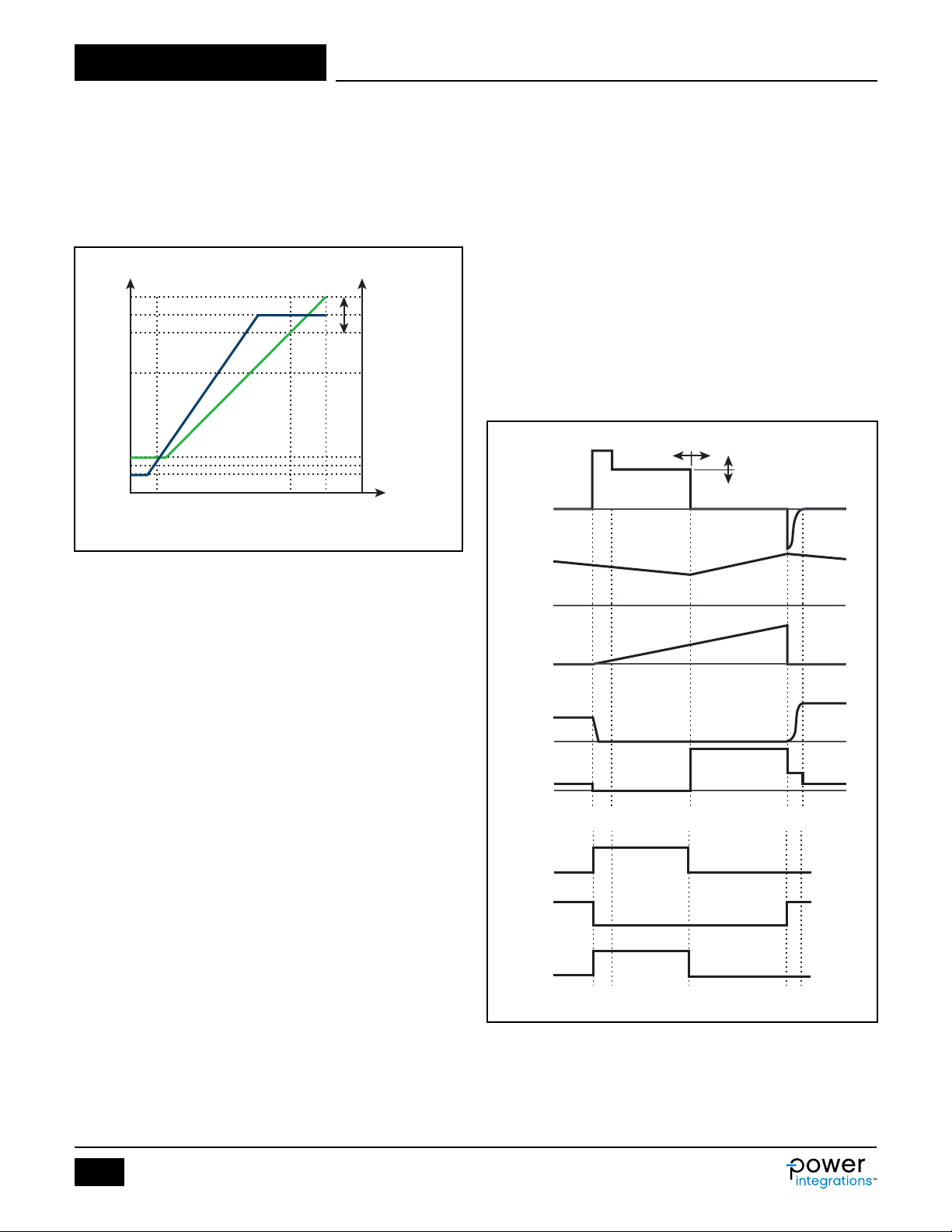
Application Note AN-69
PI-8247-011917
resulting decrease in primary resistive losses. This will have the
effect of moving the maximum load operating point to the left on
Figure 49, to around 70-75% of V
have to be done to verify that the operational specications are met
. In this case more testing will
CS(MA X)
over the production spread of component tolerances.
PI Expert tends to aim for higher efciency, so the V
point will tend to be to the left of 85% of V
F
SW
F
MAX
f
NL
r
MIN
V
CTRL(NL)
V
CTRL(FL)VCTRL(MAX)
CTRL(M AX)
CTR L(FL)
.
V
CSTHR(IPK)
V
CS(MAX)
K
CTRL(TOL)
V
CS(MAXACT)
V
CS(MIN)
PI-8155-011717
operating
V
CTRL
The extra diode only needs to be low voltage, 20 V+, and must
support the peak primary current over the duty cycle at the lowest AC
input voltage. ESD1 or UF4001 types would be suitable.
To enhance the operation of EasyStart the time period t3 – t4 of
Figure 49 should be maximized, so R
to 150 W. This will speed up the charge entering the base region and
should be reduced to 100 W
SBD
reduce t2 – t3 time period and extend t3 – t4.
A limitation of the technique is that it loses effectiveness at high-line
voltages on universal input designs. The time period t1 – t3 remains
fairly constant during start-up, but the overall period t1 – t5 reduces
with increasing HT voltage, which reduces the C
– t4. It usually remains effective at 240 VAC, but gets marginal at
recharge time t3
VCC
264 VAC. Monitoring the EMITTER DRIVE and VOLTAGE SUPPLY pins
will give a measure of the effectiveness of EasyStart at higher input
voltages.
Where difculties are experienced, reduce R
the primary inductance and the minimum input voltage.
to 100 W or increase
SBD
b
a
I
BD
Figure 49. Relationship Between Control Voltage, Switching Frequency and
VCS Threshold.
EasyStart Feature
Some adapter designs, particularly those for networking equipment,
are required to operate with a large additional capacitance, around
3000 mF, connected to the output. This is compounded by the fact
that these adapters are usually 12 V output making start-up very
challenging. For a standard design where the maximum current (CC
current) is the label output current plus 7%, the time taken to charge
the capacitance up to the label voltage at the label load current would
take a long time. This would require a large C
power the IC until the bias wind has enough voltage to recharge C
Another option is to have the maximum current much higher than the
rated load current, but this would be an expensive solution as the
transformer, at least, would have to be oversized to operate at the
higher current.
The LNK4x14D and LNK4x15D have the EasyStart feature enabled, so
a normal value of CVCC can be used, whilst allowing start-up into a
high value of output capacitance. The size of the output capacitor
that can be charged at start-up is only limited by the time allowed for
this to be achieved.
The EasyStart feature modies the timing of the BD and ED switching
cycle so that when in period t3 to t4 (BJT storage time) in Figure 46
and 50, the EMITTER DRIVE pin pull down is turned off.
An additional fast, low voltage diode is connected from the BJT
emitter to C
C
voltage level the emitter current ows into C
VCC
EasyStart only activates when VCC is below 6 V, so once the bias
, see Figure 51, so that when the emitter rises to the
VCC
winding starts powering VCC and maintaining it above the usual design
level of 8 V+, the EasyStart feature will not activate again and has no
effect on performance i.e. efciency and no-load power.
of some 10s of mF to
VCC
charging it up.
VCC
VCC
V
CC
I
ED
V
CE
.
V
ED
t1t
2
t
3
Logic
BD
Logic
BD GND
Logic
ED GND
Figure 50. Modied Base Drive and Emitter Drive Timing for EasyStart
Feature.
t4t
5
ON
OFF
ON
OFF
ON
OFF
32
Rev. B 10/17
www.power.com
Page 33
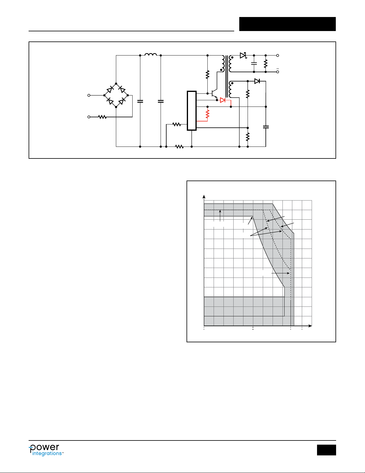
Application NoteAN-69
L
FILT
D
BRIDGE
C
~
R
IN
C
IN1
IN2
LNK4014D
R
Figure 51. Schematic with Extra Diode for EasyStart Feature.
Thermal Shut Down
The LinkSwitch-4 has a thermal shut down feature. If the junction
temperature of the IC exceeds TSD, about 140 ºC, the chip will shut
down and cease switching. Once the temperature has fallen by T
the chip will restart, perform a normal start-up cycle and continue.
SD(H)
Constant Power (CP) option
In addition to EasyStart, LNK4214D and LNK4215D devices have a
constant power section to the VI curve, see Figure 52. This feature is
intended to further improve start-up into large capacitive loads
(5000 µF at 12 V). At start-up, the constant current (CC) pull-up set
point of the VI characteristic (bottom right of Figure 52) is set by the
transformer turns ratio, the value of RCS and the value of the device
parameter V
LNK4214D and LNK4215D compared to LNK4014D and LNK4115D, so
for a given transformer and R
about 75% higher than the standard CV/CC VI curve parts, providing
. The value of V
CC(S C)
is about 75% higher on
CC(S C)
value the CC level, I
CS
OUT(EX T)
, will be
an extra 75% of start-up current into the output capacitance and
aiding a successful rapid start-up. As the output voltage rises, the
controller regulates in CC mode until it is above approximately 50% of
the design CV level. It then operates in a power limited (CP) mode
until the voltage reaches the design CV set point, at which point it
changes to CV mode regulation. I
greater than 57% of I
dependent on the HT level (mains input level). This is due to the
. The exact trajectory is somewhat
OUT(EX T)
at this point, I
OUT
OUT (CP)
, will be
controller operating in open loop mode over the CP section of the VI
curve i.e. feedback is not effective during this section, so inaccuracies
due to efciency variation over the CP section and mains input level
are not corrected. Hence there is no single CP curve for a design, but
minimum and maximum curves between which the actual curve will
lie, see I
constant power value is set by the full load switching frequency
for Low Mains and High Mains in Figure 52. The
OUTC P(TYP)
parameter FSW, the primary inductance, the peak primary current ‒
set by the device parameter V
the conversion efciency. Due to the open-loop mode of operation
divided by the value of RCS, and
CS(MA X)
on the CP section, tolerances in primary inductance, switching
frequency, RCS, V
of the CP section of the VI curve. This must be factored in when
CS(MA X)
and V
play a signicant part in the accuracy
CSCC
undertaking the design of a CP application.
D
OUT
T1
+
R
OUT
2 × R
C
OUT
HT
Q1
CS2
BD
ED
VCC
EasyStart
R
SBD
SBD
CS
FB
GND
R
CS
V
(V)
OUT
Diode
R
FB1
R
FB2
PI-8180-110916
C
VCC
,
100%
V
OUTCV(TYP)
75%
50%
33%
I
OUTCP(MIN)
I
OUTCP(TYP)
I
OUT(EXT)
100%0 175% 200%
Figure 52. Typical LNK4214D and LNK4215D CP Output Characteristic.
Low Mains
Primary inductance tolerance should be ±5% or better, F
tolerance of ±7%, V
or b e t t e r.
±2%, V
CSCC
±5.5% and RCS should be ±1%
CS(MA X)
High Mains
has a
SW
PI-7678-090215
I
(A)
OUT
www.power.com
33
Rev. B 10/17
Page 34

Application Note AN-69
IV G
21
CC OCAB
##
+
^h
IN
R
V
CS
The rst step is to use the LinkSwitch-4 PIXls tool to design the
transformer and component values for a CV/CC equivalent to the
CV/CP circuit. The important consideration is to have the CV/CP
circuit be able to provide at least the specication label output
current at the label output voltage to the load i.e. I
52 must be equal or greater than the label current across component
OUTCP(MI N)
in Figure
tolerances. Worst-case, this means that 15.5% must be allowed for.
In practice, 10% should be acceptable mainly due to parameter
tolerance safety margins in the chip and the statistics of getting the
worst case values on the same board.
Enter a value of the label output current plus 10% into [B10], otherwise follow the CV/CC design procedure described above. This will
produce a transformer and component set that will run efciently up
to the label current and if a standard CV/CC LinkSwitch-4 were to be
used, the CV to CC transition point would be at the correct level.
The LNK4214D and LNK4215D have a modied value for V
higher so that the circuit will reach the power limited CP condition
CSCC
. It is
before the CC condition and provide the VI curve given in Figure 52.
What is required is a new value for RCS to allow V
when the output is delivering the current entered in [B10], ICC at VO.
to be reached
CS(MA X)
This can be calculated from the formula:
2
LV FEff
###
R
CS
The maximum output current I
PCSMAX SW OUT
=
can be calculated from:
OUTEXT
OUTTEXT
CSCC
#=
Where:
L
= Nominal primary inductance in Henries.
P
V
= V
CS(MAX)
F
= Maximum switching frequency of LinkSwitch-4 in Hz,
SW
nominally 65000 Hz.
Eff
= Estimate of conversion efciency from primary to secondary
OUT
output. Default to 0.9 if no other gure is available via
for LinkSwitch-4 device in volts, nominally 0.36 V.
CS(MA X)
measurement.
ICC = Label rated output current plus margin, normally +10%.
VO = Label output voltage.
G
= Design cable compensation at ICC. i.e. 0.03 for 3%.
CAB
N = Transformer primary to secondary turns ratio.
V
= Constant current control reference level for the appropriate
CSCC
LinkSwitch-4 device in volts.
Due to the estimation of Eff
may have to be trimmed to obtain the correct positioning of the CV to
, the resulting value of RCS calculated
OUT
CP corner point.
It is prudent to check the resulting VI curves with transformers
gapped for the maximum and minimum primary inductance to ensure
the desired IO is met.
Check the rating of the output diode, the output current can now be
75% higher than a CV/CC design, though it may only be during
start-up, depending on usage.
The CP parts also have the EasyStart function, so the EasyStart diode
must be used or the LinkSwitch-4 will be damaged.
Primary Current
Sense Threshold
for CC Operation V
CSCC
Device Min Typ Max Units
Except LNK4115D, LNK4214D, LNK4215D -62 -60.8 -59.6
LN K4115 D only -68
mV
LN K4214D o nly -105
LNK4215D on ly -119
34
Rev. B 10/17
www.power.com
Page 35

Notes
Application NoteAN-69
www.power.com
35
Rev. B 10/17
Page 36

Revision Notes Date
A Initial Release. 01/17
B Updated Figure 34. 10/17
For the latest updates, visit our website: www.power.com
Power Integrations reserves the right to make changes to its products at any time to improve reliability or manufacturability. Power Integrations
does not assume any liability arising from the use of any device or circuit described herein. POWER INTEGRATIONS MAKES NO WARRANTY
HEREIN AND SPECIFICALLY DISCLAIMS ALL WARRANTIES INCLUDING, WITHOUT LIMITATION, THE IMPLIED WARRANTIES OF MERCHANTABILITY,
FITNESS FOR A PARTICULAR PURPOSE, AND NON-INFRINGEMENT OF THIRD PARTY RIGHTS.
Patent Information
The products and applications illustrated herein (including transformer construction and circuits external to the products) may be covered by one
or more U.S. and foreign patents, or potentially by pending U.S. and foreign patent applications assigned to Power Integrations. A complete list of
Power Integrations patents may be found at www.power.com. Power Integrations grants its customers a license under certain patent rights as set
forth at http://www.power.com/ip.htm.
Life Support Policy
POWER INTEGRATIONS PRODUCTS ARE NOT AUTHORIZED FOR USE AS CRITICAL COMPONENTS IN LIFE SUPPORT DEVICES OR SYSTEMS
WITHOUT THE EXPRESS WRITTEN APPROVAL OF THE PRESIDENT OF POWER INTEGRATIONS. As used herein:
1. A Life support device or system is one which, (i) is intended for surgical implant into the body, or (ii) supports or sustains life, and (iii) whose
failure to perform, when properly used in accordance with instructions for use, can be reasonably expected to result in signicant injury or
death to the user.
2. A critical component is any component of a life support device or system whose failure to perform can be reasonably expected to cause the
failure of the life support device or system, or to affect its safety or effectiveness.
The PI logo, TOPSwitch, TinySwitch, SENZero, SCALE-iDriver, Qspeed, PeakSwitch, LYTSwitch, LinkZero, LinkSwitch, InnoSwitch, Hip e rT FS,
HiperPFS, HiperLCS, DPA-Switch, CAPZero, Clampless, EcoSmart, E-Shield, Filterfuse, FluxLink, StakFET, PI Expert and PI FACTS are trademarks of
Power Integrations, Inc. Other trademarks are property of their respective companies. ©2017, Power Integrations, Inc.
Power Integrations Worldwide Sales Support Locations
World Headquarters
5245 Hellyer Avenue
San Jose, CA 95138, USA
Main: +1-408-414-9200
Customer Service:
Phone: +1-408-414-9665
Fax: +1-408-414-9765
e-mail: usasales@power.com
China (Shanghai)
Rm 2410, Charity Plaza, No. 88
North Caoxi Road
Shanghai, PRC 200030
Phone: +86-21-6354-6323
Fax: +86-21-6354-6325
e-mail: chinasales@power.com
China (Shenzhen)
17/F, Hivac Building, No. 2, Keji Nan
8th Road, Nanshan District,
Shenzhen, China, 518057
Phone: +86-755-8672-8689
Fax: +86-755-8672-8690
e-mail: chinasales@power.com
Germany
Lindwurmstrasse 114
80337 Munich
Germany
Phone: +49-895-527-39110
Fax: +49-895-527-39200
e-mail: eurosales@power.com
Germany
HellwegForum 1
59469 Ense
Germany
Tel: +49-2938-64-39990
e-mail: igbt-driver.sales@
power.com
India
#1, 14th Main Road
Vasanthanagar
Bangalore-560052 India
Phone: +91-80-4113-8020
Fax: +91-80-4113-8023
e-mail: indiasales@power.com
Italy
Via Milanese 20, 3rd. Fl.
20099 Sesto San Giovanni (MI) Italy
Phone: +39-024-550-8701
Fax: +39-028-928-6009
e-mail: eurosales@power.com
Japan
Yusen Shin-Yokohama 1-chome Bldg.
1-7-9,, Shin-Yokohama, Kohoku-ku
Yokohama-shi, Kanagawa
222-0033 Japan
Ph one: +81-45 - 471-1021
Fax: +81- 45- 471-3717
e-mail: japansales@power.com
Korea
RM 602, 6FL
Korea City Air Terminal B/D, 159-6
Samsung-Dong, Kangnam-Gu,
Seoul, 135-728, Korea
Phone: +8 2-2-2016 -6610
Fax: +82-2-2016-6 630
e-mail: koreasales@power.com
Singapore
51 Newton Road
#19-01/05 Goldhill Plaza
Singapore, 308900
Phone: +65-6358-2160
Fax: +65-6358-2015
e-mail: singaporesales@power.com
Taiwan
5F, No. 318, Nei Hu Rd., Sec. 1
Nei Hu Dist.
Taipei 11493, Taiwan R.O.C.
Phone: +8 86-2-2659-4570
Fax: +886-2-2659-4550
e-mail: taiwansales@power.com
UK
Building 5, Suite 21
The Westbrook Centre
Milton Road
Cambridge
CB4 1YG
Phone: +44 (0) 7823-557484
e-mail: eurosales@power.com
 Loading...