

Page 1
®
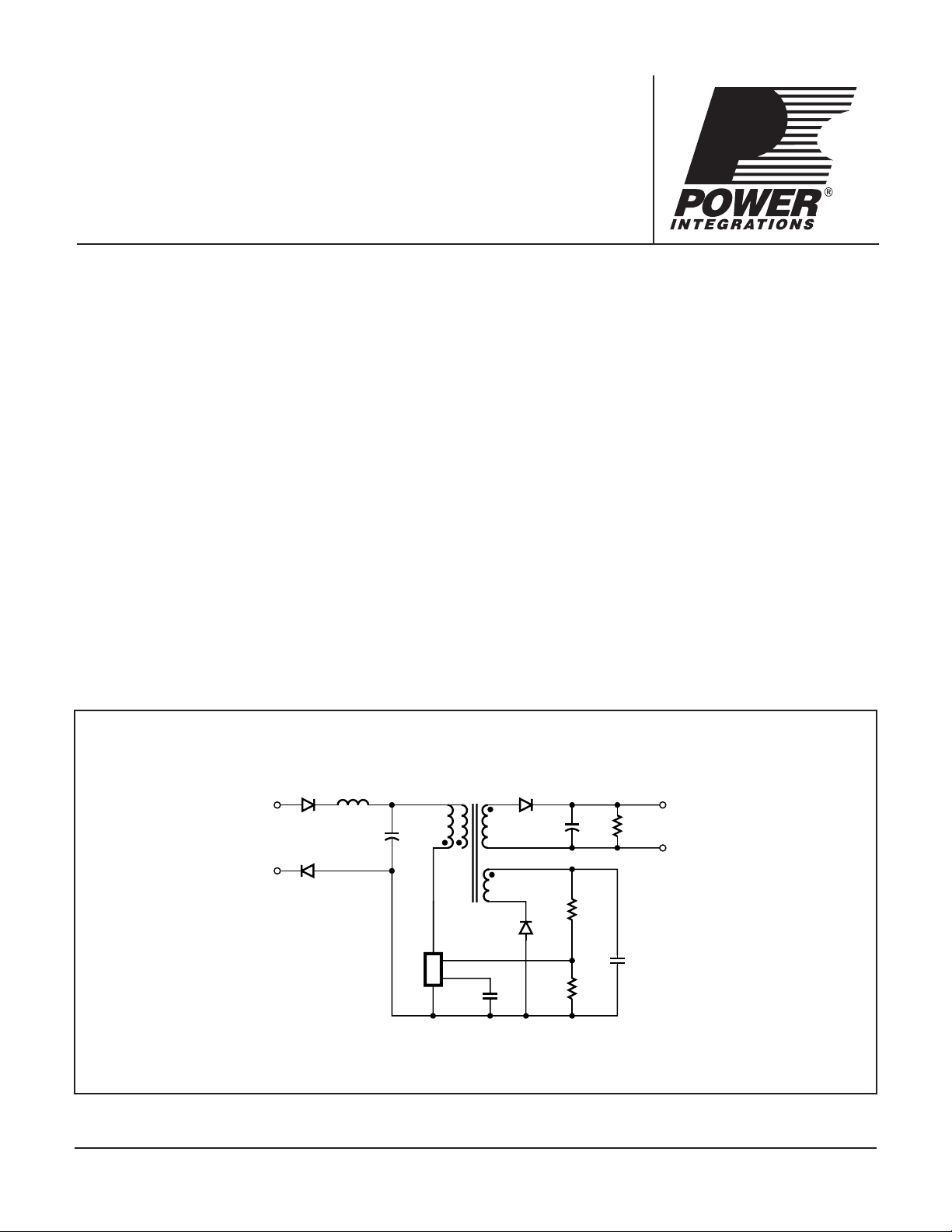
D
S
FB
BP
RTN
6 V,
0.33
A
L
N
D1
1N4937
C1
10 µF
400 V
C3
0.1
µF
50 V
L1
3.3 mH
D6
UF4002
D5
1N4005
C5
220 µF
25 V
C4
0.33 µF
50 V
R4
2 kΩ
R1
37.4 kΩ
R2
3 kΩ
T1
EE16
2
1
7
6
4
5
D4
1N4007
90-265
VAC
LinkSwitch
PI-4063-101005
U1
LNK564P
LinkSwitch-LP
Flyback Design Guide
Application Note AN-39
Introduction
The LinkSwitch-LP family is designed to replace inefficient
line frequency linear transformer based power supplies with
output powers < 2.5 W in applications such as cell/cordless
phones, PDAs, digital cameras, and portable audio players.
LinkSwitch-LP may also be used as auxiliary supplies employed
in applications such as white goods.
LinkSwitch-LP combines a high voltage power MOSFET switch
with an ON/OFF controller in one device. It is completely
self-powered from the DRAIN pin, has a jittered switching
frequency for low EMI and is fully fault protected. Auto-restart
limits device and circuit dissipation during overload and output
short circuit conditions while hysteretic over-temperature
protection disables the internal MOSFET during thermal
faults. EcoSmart® technology enables designs to easily attain
< 150 mW no-load consumption, meeting worldwide energy
efficiency requirements.
LinkSwitch-LP is designed to operate without the need for a
primary-side clamp circuit for output powers below 2.5 W and
thus, dramatically reduces component count and total system
cost. Figure 1 shows a
LinkSwitch-LP based 2 W power supply
without a primary-side clamp. The LinkSwitch-LP family
has been optimized to give an approximate CV/CC output
characteristic when feedback is provided from an auxillary or
bias winding on the transformer. This is ideal for applications
replacing a line frequency transformer, providing a compatible
output characteristic but with reduced overload, short circuit
current and variation with input line voltage.
Scope
This application note is for engineers designing an isolated
AC-DC flyback power supply using the LinkSwitch-LP family of
devices. It provides guidelines to enable an engineer to quickly
select key components and complete a transformer design for an
application requiring either a constant voltage (CV) or constant
voltage and constant current (CV/CC) output. To simplify the
task of transformer design, this application note refers directly
to the PI Xls design spreadsheet that is part of the PI Expert™
design software suite.
Figure 1. Basic Circuit Schematic Using LinkSwitch-LP in a Clampless™ Design.
July 2006
Page 2
AN-39
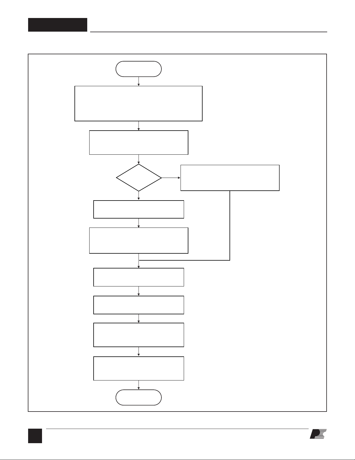
Enter power supply specifications:
Input voltage range and frequency, output voltage,
output current and VI characteristic, feedback type,
loss allocation factor, diode conduction time and
input capacitance
Select LinkSwitch-LP based on Table 4
(see data sheet) and reflected
output voltage (VOR) to 80 V
Select a standard transformer design
(Table 8). See appendices for
Transformer and bobbin drawings
Select transformer core and bobbin
based on Table 5 and 6
Select input stage filter and rectifier
based on Table 7
Select BYPASS pin capacitor. Use
0.1 µF / 50 V capacitor. See Step 6
Ensure that flux density BM < 1500
Gauss (150 mT). Adjust by
increasing number of secondary turns NS
Select output diode based on
Table 8 and calculate preload
resistor
Select output capacitor based on
secondary ripple current and
output voltage (see Step 8)
PI-4137-101005
Start design
Finish design
4 V ≤ VO ≤ 12 V
PO ≤ 2 W
Yes
No
Quick Start
Figure 2. LinkSwitch-LP Flyback Design Flowchart.
B
7/06
2
Page 3
Step-by-Step Design procedure
I
OUT
I
OUTIOUT
V
OUT
V
OUT(TYP)
Maximum Peak
Power Point
Nominal Peak
Power Point
PI-4152-100705
I
O
I
OUT(TYP)
V
OUT(TYP)
V
O
Maximum Peak
Power Point
Nominal Peak
Power Point
PI-4172-101005
AN-39
Step 1 – Enter Application Variables: VAC
MIN
, VAC
MAX
fL, VO, IO, CV/CC spec, PO, Clamp and Feedback type,
η, Z, tC and CIN.
Determine the input voltage range (VAC
and VAC
MIN
MAX
) from
Table 1.
Nominal Input Voltage VAC
MIN
VAC
MAX
100/115 85 132
230 195 265
Universal 85 265
Table 1. Standard Worldwide, Input Line Voltage Ranges.
Line Frequency, f
L
Enter the worst-case line frequency under which the supply
should operate normally.
Output Voltage, V
O
Enter the output voltage. For loose CV/CC designs, this should
be the typical output voltage at the nominal peak power point in
the output characteristic. For CV only outputs this should be the
specified output voltage. For designs with an output cable enter
the voltages at the load. For multiple output designs enter the
voltage for the main output from which feedback is taken.
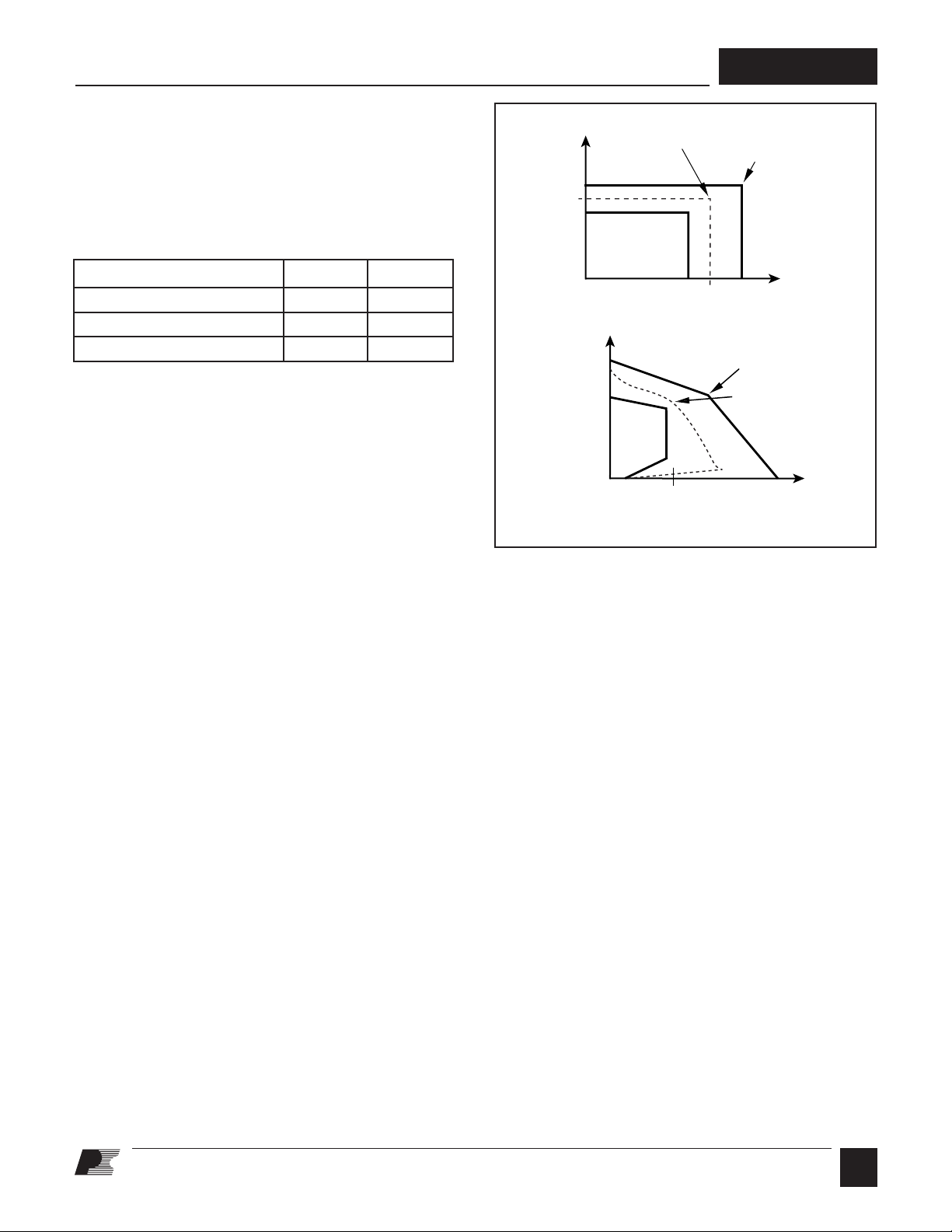
,
(a)
(b)
Figure 3. Diagram Showing Correct Values of IO and VO to enter
in the spreadsheet for (a) Optocoupler Feedback and (b)
Bias Winding Feedback
Output Current, I
O
For loose CV/CC designs, this should be the typical output current
at the nominal peak power point in the output characteristic.
For CV only outputs, this should be the maximum specified
output current. In multiple output designs, the output current
of the main output (typically the output from which feedback
is taken) should be increased such that PO matches the sum
of the output powers from all the outputs in the design. The
individual output voltages and currents should then be entered
at the bottom of the spreadsheet.
CC portions of the spec. This arrangement uses bias winding
feedback to regulate the output. During normal operation
switching cycles are enabled or disabled to maintain the voltage
at the FEEDBACK pin. This, via the turns ratio between the
bias and secondary windings regulates the output. However
as the secondary output voltage is not directly sensed, errors
caused by leakage inductance and resistive drops result is
only moderate load regulation (however still better than an
unregulated line frequency linear transformer based supply).
Once the maximum power point is reached (determined by the
primary inductance, current limit and switching frequency) the
Figure 3 shows a diagram with correct values of I
and VO to
O
enter in the spreadsheet for both Optocoupler based feedback
and Bias Winding Feedback.
voltage on the bias winding begins to fall and the switching
frequency of LinkSwitch-LP is reduced to limit the maximum
output current as an output overload increases toward a short
circuit.
CV/CC Output Specification
If the output specification is loose constant voltage and constant
current (charger) CV/CC type enter ʻYESʼ in cell B8, otherwise
enter ʻNOʼ for Constant voltage (adapter) CV only. For CV/CC
designs, the typical value of I
2
f is used in the computation of
primary inductance, while for CV only designs, the minimum
value of I2f is used to guarantee power delivery.
A CV/CC characteristic can be achieved by using either one
of the arrangements shown in Figures 1 or 4. Figure 1 shows
a low cost primary side control scheme for both the CV and
For improved performance, Figure 4 shows an arrangement
using an optocoupler and high gain voltage reference IC (U2)
to regulate the output voltage. Once the maximum power
point is reached and the output voltage falls, the output current
is controlled via the bias winding, sensed via R
and RY
X
(Figure 4). As shown in Table 3 the high gain of the system
gives an output voltage with minimal variation during CV
operation and good linearity, maintaining an almost vertical CC
characteristic. As the output is being sensed indirectly via the
bias winding during CC operation, the CC characteristic is still
B
7/06
3
Page 4
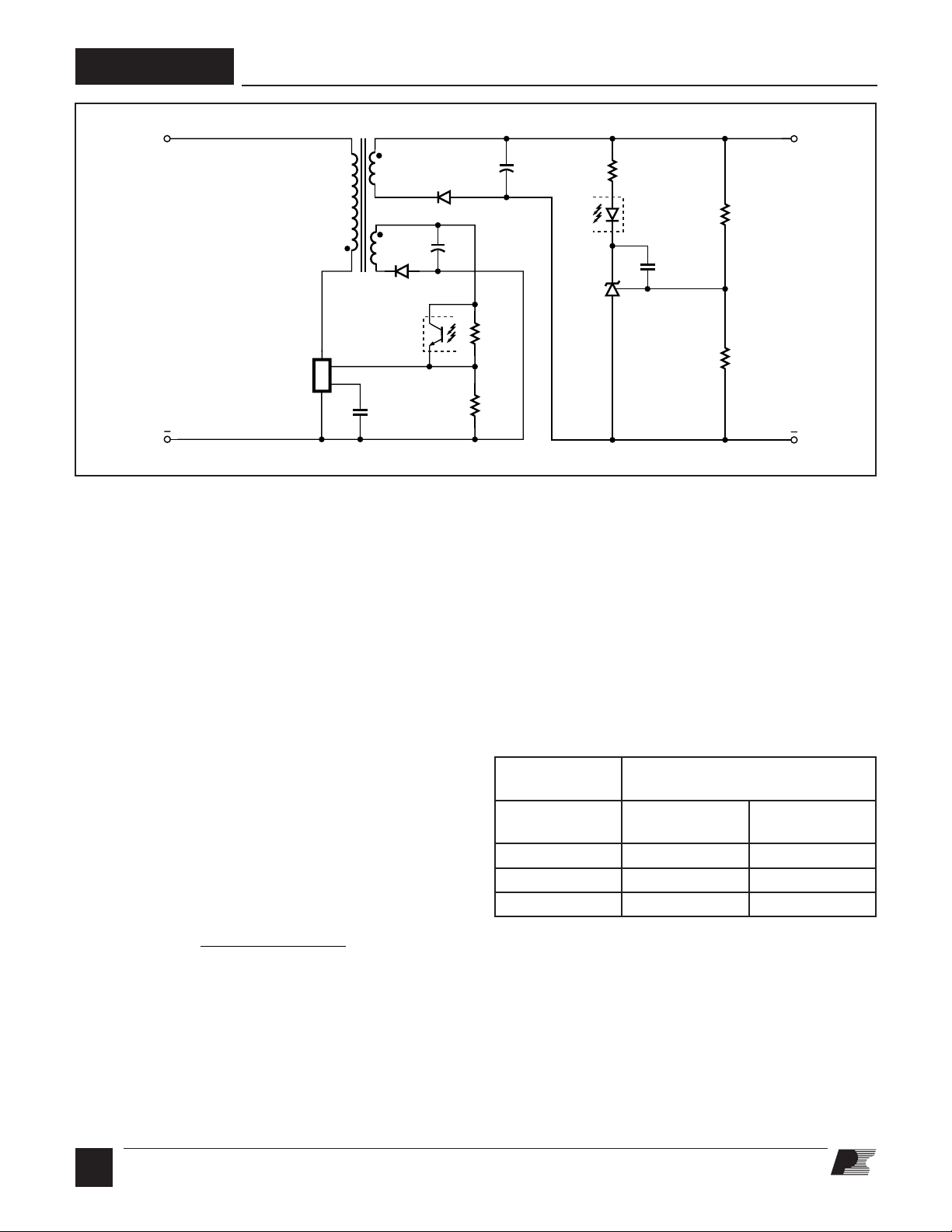
AN-39
Z
Total Losse
s
Secondary Side Losses
=
T1
+
+
D
S
FB
BP
DC BUS
or
HV DC
V
O
R
X
D
B
D
S
C
B
C
O
R
Y
R
3
R
1
R
2
U1
LNK564P
0.1 µF
50 V
0.33
µF
50 V
U2
LinkSwitch-LP
PI-4138-070706
Figure 4. Circuit Schematic for High Performance CV/CC Output Characteristic.
subject to unit-to-unit variation caused by the difference in the
transformer (bias to secondary coupling and leakage inductance.
Also see Enter Feedback, Bias Type and Clamp Information
section). Note that the reference IC U2 may be replaced by a
lower cost zener diode in applications where increased tolerance
is acceptable during CV operation.
Finally for improved CC performance a secondary CC sense
circuit can be used. This removes variation in the CC due to
the transformer and FEEDBACK pin.
Power Supply Efficiency,
Enter the estimated power supply efficiency measured at the
point of load. For both CV/CC and CV only designs use 0.65 if
no better data is available or until measurements can be made
on a prototype.
Power Supply Loss Allocation Factor, Z
This factor represents the proportion of losses between the
primary and the secondary of the power supply.
If no better data is available then the following values are
recommended:
• Bias winding feedback designs (CV or CV/CC): 0.5 (0.35)
• Optocoupler CV feedback and/or bias winding CC
feedback: 0.5 (0.35)
• Optocoupler CV and CC feedback: 0.75 (0.6)
4
B
7/06
For designs using Filterfuse™ use the values in parenthesis,
these take into account the additional primary side losses due
to a typical value of ~50 Ω for the resistance of the Filterfuse
inductor
Bridge Diode Conduction Time, t
(ms)
C
Enter the bridge diode conduction time. Use 3 ms if no other
data is available.
Total Input Capacitance C
(µF)
IN
Enter total input capacitance using Table 2 for guidance.
η
Total Input Capacitance per Watt
of Output Power (µF/W)
AC Input
Voltage (VAC)
Half Wave
Rectification
Full Wave
Rectification
100/115 5-8 3-4
Table 2. Suggested Total Input Capacitance for Different Input
Voltage Ranges.
The capacitance should be selected to keep the minimum DC
input voltage, V
Note: For designs that have a DC rather than an AC input, the
value of the minimum and maximum DC input voltages, V
and V
on the design spreadsheet (see Figure 5).
230 1-2 1
85-265 5-8 3-4
> 50 V and ideally > 70 V.
MIN
, may be entered directly into the gray override cells
MAX
MIN
Page 5
AN-39
PI-4140-101305
8
7
6
5
4
3
2
1
0
0 150 450300 600 750
Load (mA)
Output Voltage (V)
9
8
7
6
5
4
3
2
1
0
0 150 450300 600 750
Load (mA)
PI-4139-092205
Output Voltage (V)
9
8
7
6
5
4
3
2
1
0
0 150 450300 600 750
Load (mA)
PI-4173-101305
Output Voltage (V)
9
ENTER APPLICATION VARIABLES
Customer
VACMIN 85 Volts
Minimum AC Input Vo
ltage
VACMAX 265 Volts
Maximum AC Input Vo
ltage
fL 50 Hertz
AC Mains Frequency
VO 6.00 Volts
Output Voltage (main) measured at the end of output cable (For CV/CC designs enter typical CV
tolerance limit
)
IO 0.33 Amps
Power Supply Output Current (For CV/CC designs enter typical CC tolerance limit)
Constant Voltage / Constant Current Output YES CVCC Volts
Enter "YES" for approximate CV/CC output. Enter "NO" for CV only output
Output Cable Resistance
0.16 0.16 Ohms
Enter the resistance of the output cable (if used)
PO 2.00 Watts
Output Power (VO x IO + dissipation in output cable)
Feedback Ty
pe BIAS
Bias
Winding Enter 'BIAS' for Bias winding feedback and 'OPTO' for Optocoupler feedback
Add Bias Winding
YES Yes
Enter 'YES' to add a Bias winding. Enter 'NO' to continue design without a Bias winding. Addition of
Bias winding can lower no load consumptio
n
Clampless design YES
Clampless
Enter 'YES' for a clampless design. Enter 'NO' if an external clamp circuit is used
.
n 0.64
Efficiency Estimate at output terminals. For CV only designs enter 0.7 if no better data available
Z 0
.35 0.35
Loss Allocation Factor (Secondary side losses / To
tal losses)
tC 2.90 mSeconds
Bridge Rectifier Conduction Time Estimat
e
CIN 9
.40 uFarads
Input Capacitance
Input Rectification Ty
pe F
F
Choose H for Half Wave Rectifier and F for Full Wave Rectification
DC INPUT VOLTAGE PARAMETERS
VMIN 99 Volts
Minimum DC Input Voltag
e
VMAX 375 Vo
lts
Maximum DC Input Voltag
e
Bias Winding Feedback
(Figure 1)
Optocoupler with Zener
as Reference (Figure 4, U2
Replaced with Zener
Optocoupler with TL-431 as
Reference (Figure 4)
Typical Output
Characteristics
Cost Low Higher Highest
Component count
Lowest component count Higher component count Highest component count
Ease of Design High Medium Medium
CV/CC Tolerance
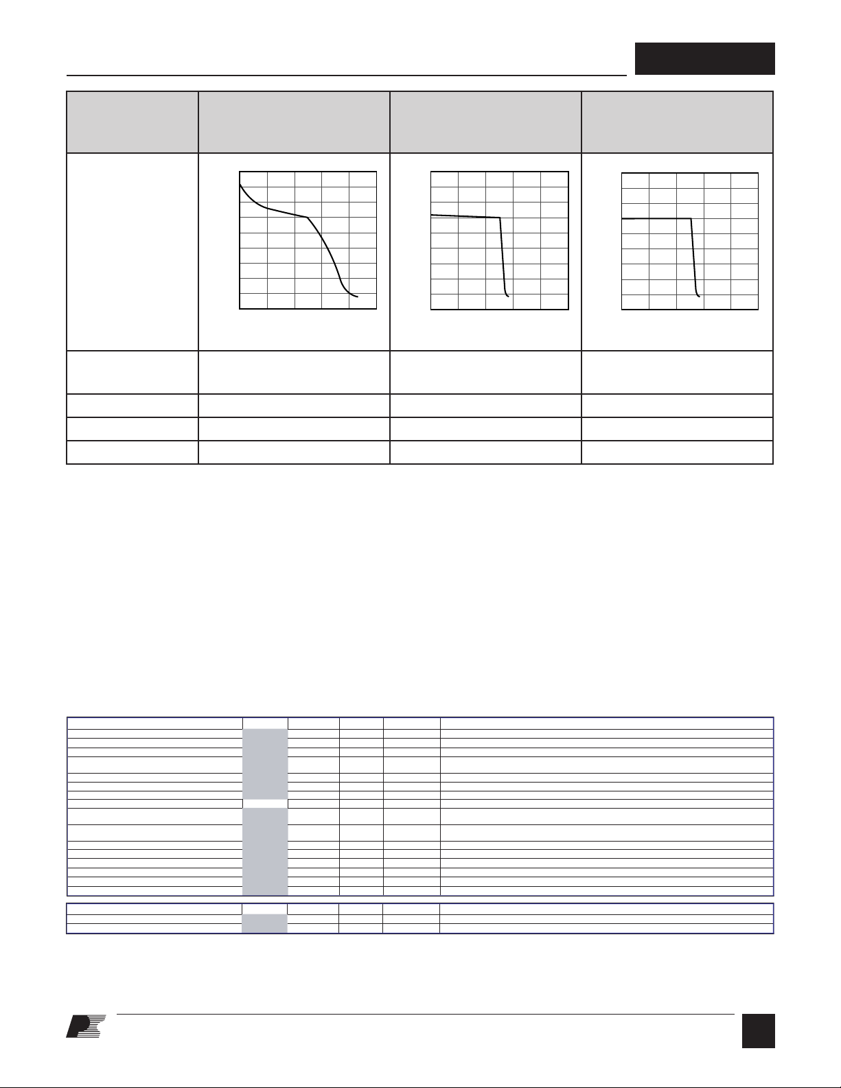
Table 3. Summary of Comparison Between Bias Winding Feedback and Optocoupler Feedback.
Good Better Best
Enter Feedback, Bias Type and Clamp Information
Select either bias winding feedback (primary-side feedback)
as shown in Figure 1or optocoupler feedback (secondary-side
feedback) as shown in Figure 4. Bias winding feedback makes
use of a primary-side auxiliary winding to set the output voltage.
Optocoupler feedback directly senses the output voltage and
can provide any level of accuracy depending on the voltage
reference selected. Both primary-side feedback and secondaryside feedback allow for a CV/CC output characteristic. See
Table 3 for a summary of feedback types.
Figure 5. Application Variable Section of LinkSwitch-LP Design Spreadsheet.
If optocoupler feedback is selected, the user still has the option
to reduce overall power consumption by using a bias winding
to power the optocoupler transistor. That bias winding can also
be configured as a shield, for improved EMI performance.
Clampless™ designs typically exhibit a resonance between the
leakage inductance and primary capacitance, that is normally
damped by the primary clamp. As there is less damping in a
Clampless design this creates a peak in the conducted EMI
measurements in 1-4 MHz range. It is generally the EMI
7/06
B
5
Page 6

AN-39
ENTER LinkSwitch-LP VARIABLES
LinkSwitch-LP
LNK564
LinkSwitch-LP device
Chosen Device
LNK564
ILIMITMIN 0.124 Amps
Minimum Current Limit
ILIMITMAX 0.146 Amps
Maximum Current Limi
t
fSmi
n 93000 Hertz
Minimum Device Switching Frequenc
y
I^2fMIN 1665 A^2Hz
I^2f Minimum value (product of current limit squared and frequency is trimmed for tighter tolerance)
I^2fTYP 1850 A^2Hz
I^2f typical value (product of current limit squared and frequency is trimmed for tighter tolerance)
VOR
80 Volts
Reflected Output Voltag
e
VD
S 10 Volts
LinkSwitch-LP on-state Drain to Source Voltage
VD 0.5 Vo
lts
Output Winding Diode Forward Voltage Drop
KP 1.53
Ripple to Peak Current Ratio (0.9<KRP<1.0 : 1.0<KDP<6.0)
performance and not the peak drain voltage that limits the use
of Clampless designs to < 2 W. However if a bias winding is
added which uses a slow diode (1N400x series) that peak in
EMI is reduced as the bias acts as a clamp, damping out the
leakage inductance ringing. This extends the power range for
Clampless designs to ≤2.5 W. In addition, the use of a small
Y-Capacitor (100 pF) can be beneficial in containing this problem
and making the EMI performance less variable.
For designs greater than 2.5 W, a
Clampless solution is not
recommended.
The guidance above applies to universal input or 230 VAC only
designs. For 100/110 VAC only input designs it may be possible
to use Clampless designs above 2 - 2.5 W but only after verifying
acceptable peak drain voltage and EMI performance.
All the variables described above can be entered in the Enter
Application Variables section of the
LinkSwitch-LP design
spreadsheet in the PI Xls design software (see Figure5).
Step 2 – Enter LinkSwitch-LP, VOR, VDS, V
D
Select the appropriate LinkSwitch-LP based on the input
voltage range and the corresponding maximum output power
(see Table 4 & 5).
Maximum Power (W)
Device Universal Input 230 VAC
LNK562 1.9 1.9
LNK563 2.5 2.5
LNK564 3 3
Table 4. Maximum Output Power Capability of LinkSwitch-LP
Devices.
Power delivery from a given device also depends on the
transformer core size selected. Table 5 provides examples of
the output power possible from each device and 3 common
core sizes. These power numbers assume a flux density of
1500 Gauss, and can be increased for higher flux densities,
based on acceptable audible noise.
Reflected Output Voltage, V
OR
(V)
This parameter is the secondary winding voltage reflected
back to the primary through the turns ratio of the transformer
(during the off time of the LinkSwitch-LP). The default
value is 80 V, however this can be increased up to 120 V to
achieve the maximum power capability from the selected
LinkSwitch-LP device. In general, start with the default value of
80 V, increasing the value when necessary to maintain KP above
its lower limit of 0.9 at the minimum input voltage of 85 VAC.
For Clampless designs, there is less flexibility in selecting the
value of VOR. Increasing VOR directly increases the peak drain
voltage. Therefore for Clampless designs, a value of 80 V should
be used and only increased once the peak drain voltage has been
measured and adequate margin to BV
determined.
DSS
LinkSwitch-LP On-State DRAIN-to-SOURCE Voltage,
VDS (V)
This parameter is the average on-state voltage developed across
the DRAIN and SOURCE pins of LinkSwitch-LP. By default, if
the gray override cell is left empty, a value of 10 V is assumed.
Use the default value if no better data is available.
Output Diode Forward Voltage Drop, V
(V)
D
Enter the average forward voltage drop of the (main) output
diode. Use 0.5 V for a Schottky diode or 1 V for a PN diode
if no better data is available. By default, a value of 0.5 V is
assumed.
Calculated Ripple to Peak Current Ratio, K
P
KP is a measure of the operating mode and primary current
waveshape of the design. KP < 1 indicates a continuous design
(the lower the KP, the more continuous the design) and a
KP > 1 indicates a discontinuous design (the higher the KP, the
more discontinuous the design).
Below a value of 1, indicating continuous conduction mode,
KP is the ratio of ripple to peak primary current (KRP). Above
a value of 1, indicating discontinuous conduction mode, KP is
the ratio of primary MOSFET off time to the secondary diode
conduction time (KDP). The value of KP should be in the range
of 0.9 < KP < 6 and guidance is given in the comments cell if
the value is outside this range.
B
7/06
6
Figure 6. LinkSwitch-LP Variables Section of LinkSwitch-LP Design Spreadsheet.
Page 7

AN-39
ENTER TRANSFORMER CORE/CONSTRUCTION VARIABLES
Core Type EE16
Suggested smallest commonly available core
Core
EE16 P/N:
PC40EE16-Z
Bobbin
EE16_BOBBIN P
/N:
EE16_BOBBIN
AE 0.192 cm^2
Core Effective Cross Sectional Area
LE 3.5 cm
Core Effective Path Length
AL 1140 nH/T^2
Ungapped Core Effective Inductance
BW 8.6 mm
Bobbin Physical Winding Width
M 0 mm
Safety Margin Width (Half the Primary to Secondary Creepage Distance
)
L 2
Number of primary layer
s
NS 12
Number of Secondary Tu
rns
NB 37
Number of Bias winding turns
VB 19.77 Volts
Bias Winding Voltage
R1 32.95 k-ohms
Resistor divider component between bias wiinding and FB pin of LinkSwitch-L
P
R2 3.00 k-ohms
Resistor divider component between FB pin of LinkSwitch-LP and primary RT
N
Recommended Bias Diode 1N4003
Place this diode on the return leg
of the bias winding for optimal EMI. See LinkSwitch-LP Design guide
for more information
Variables referenced in Step two are found in the Enter
LinkSwitch-LP Variables section of the spreadsheet (see
Figure 6).
Step 3 – Choose Core and Bobbin Based on Output
Power and Enter A
, Le, AL, BW, M, L, N
e
S
Core Effective Cross-Sectional Area, Ae (cm2), Core Effective
Path Length, Le (cm), Core Ungapped Effective Inductance, AL
(nH/Turn2), Bobbin Width, BW (mm).
By default, if the Core Type cell is left empty, the spreadsheet
will select the EE16 core. The user can change this selection
and choose an alternate core from a list of commonly available
cores (shown in Table 6). Table 5 provides guidance on the
power capability of specific core sizes.
Output Power Capability (W)
Core Size LNK562 LNK563 LNK564
EE13 1.1 1.4 1.7
EE16 1.3 1.7 2
EE19 1.95 2.55 3
Table 5. Typical Output Power Capability of LinkSwitch-LP
Devices vs. Core Sizes (1500 Gauss/150 mT).
Transformer Core
EE8 EE1616
EP10 EF16
EE10 EE19
EF12.6 EF20
EE13 EF25
EE16
Table 6. List of Cores Provided in LinkSwitch-LP Spreadsheet.
The gray override cells can be used to enter the core and bobbin
parameters directly. This is useful if a core is selected that is
not on the list or the specific core or bobbin information differs
from that recalled by the spreadsheet.
Safety Margin, M (mm)
For designs that require isolation but are not using triple
insulated wire for the secondary winding, the width of the safety
margin to be used on each side of the bobbin should be entered
here. Typically, for universal input designs, a total margin of
6.2 mm would be required. Therefore a value of 3.1 mm would
be entered into the spreadsheet. For vertical bobbins, the margin
may not be symmetrical.
As the margin reduces the available area for the windings,
margin construction may not be suitable for small core sizes.
If after entering the margin, more than 4 primary layers (L) are
required, it is suggested that either a larger core be selected or
switch to a zero margin design using triple-insulated wire for
the secondary winding.
Primary Layers, L
By default, if the override cell is empty, a value of 2 is assumed.
Primary layers should be in the range of 1
< L < 4 and in general,
it should be the lowest number that meets the primary current
density limit (CMA) of 150 Cmils per amp. Values above 4
layers are possible, but the increased leakage inductance and
physical fit of the windings should be considered.
For Clampless designs, 2 primary layers must be used. This is
to ensure sufficient primary capacitance to limit the peak drain
voltage below the BV
rating of the MOSFET internal to the
DSS
LinkSwitch-LP.
Secondary Turns, N
S
By default, if the gray override cell is left blank, the minimum
number of secondary turns is calculated such that the maximum
operating flux density, BM, is kept below the recommended
maximum. In general, it is not necessary to enter a number in
the override cell except in designs where a higher operating flux
density is acceptable (see Minimizing Audible Nose section for
an explanation of BM limits).
Figure 7. Transformer Core and Construction Variables Section of LinkSwitch-LP Spreadsheet.
B
7/06
7
Page 8

AN-39
TRANSFORMER PRIMARY DESIGN PARAMETERS
LP 2857 uHenries
Typical Primary Inductance. +/- 10%
LP_TOLERANCE 10 %
Primary inductance tolerance
NP 148
Primary Winding Number of Turns
ALG 131 nH/T^2
Gapped Core Effective Inductance
BM 1471 Gauss
Maximum Operating Flux Density, BM<1500 is recommended
BAC 581 Gauss
AC Flux Density for Core Loss Curves (0.5 X Peak to Peak)
ur 1654
Relative Permeability of Ungapped Core
LG 0.16 mm
Gap Length (Lg > 0.1 mm)
BWE 17.2 mm
Effective Bobbin Width
OD 0.12 mm
Maximum Primary Wire Diameter including insulation
INS 0.03 mm
Estimated Total Insulation Thickness (= 2 * film thickness)
DIA 0.09 mm
Bare conductor diameter
AWG 40 AWG
Primary Wire Gauge (Rounded to next smaller standard AWG value)
CM 10 Cmils
Bare conductor effective area in circular mils
CMA 197 Cmils/Amp
Primary Winding Current Capacity (150 < CMA < 500)
Calculated Bias Winding Turns and Voltage NB, V
B
When a bias winding is used, the number of turns and voltage
developed by the winding are displayed. The relatively large
default number of turns allows the bias to be used as a shield
winding for reduced EMI.
The variables described in Step 3 are found in the Enter
Transformer Core/Construction Variables section of the
spreadsheet (see Figure 7).
Step 4 – Iterate Transformer Design and Generate
Transformer Design Output
Iterate the design, making sure that no warnings are displayed.
Any parameters outside the recommended range of values can
be corrected by following the guidance given in the right hand
column.
Once all warnings have been cleared, the transformer design
parameters can be used to either wind a prototype transformer
or send to a vendor for samples.
The key transformer electrical parameters are:
Primary Inductance, LP (µH)
This is the target nominal primary inductance of the transformer.
For designs that use bias winding feedback, there is no current
sense resistor, and the value of primary inductance (LP)
determines the onset of the constant current (CC) portion of
the CV/CC characteristic.
Primary Inductance Tolerance, L
P_TOLERANCE
(%)
This is the assumed primary inductance tolerance. A value of
±10% is used by default, however if specific information is known
from the transformer vendor, then this may be overridden by
entering a new value in the gray override cell. For designs that
use bias winding feedback, the L
P_TOLERANCE
determines a large
part of the total CC tolerance of the output characteristic.
Maximum Operating Flux Density, B
(Gauss)
M
It is recommended that this value be below 1500 Gauss
(150 mT) during normal operation. Flux densities above
1500 Gauss (150 mT) may produce audible noise from the
transformer and for such designs the acceptability should be
verified. To minimize audible noise all transformers should be
dip varnished. Vacuum impregnation is not recommended due
to the resultant increase in winding capacitance. Flux densities
above 3000 Gauss (300 mT) are not recommended.
Other transformer parameters calculated in the spreadsheet
are:
NP - Primary Winding Number of Turns
ALG (nH/T2) - Gapped Core Effective Inductance
BAC (Gauss) - AC Flux Density for Core Loss Curves
(0.5 × Peak-to-Peak)
µr - Relative Permeability of Ungapped Core
LG (mm) - Gap Length (LG > 0.1 mm).
BWE (mm) - Effective Bobbin Width (accounts for margin
tape, if used)
OD (mm) - Maximum Primary Wire Diameter (including
insulation)
INS (mm) - Estimated Total Insulation Thickness (= 2 × film
thickness)
DIA (mm) - Bare Conductor Diameter
AWG - Primary Wire Gauge (rounded to next smaller
standard AWG value)
CM (Cmils) - Bare conductor effective area in circular mils
CMA (Cmils/Amp) - Primary Winding Current Capacity
(150 < CMA < 500)
Variables described in Step 4 can be found under the
“Transformer Primary Design Parameters” section of the
spreadsheet (see Figure 8).
Step 5 – Selection of Input Stage
The input stage comprises a fusible element(s), input rectification
and line filter network. The fusible element can be either a
fusible resistor, a fuse or make use of Power Integrationʼs
Filterfuse technique. Here, the input inductor may also be
used as a fuse, typically requiring the addition of a heatshrink
shroud to prevent incandescent material being ejected during a
fault. By using Filterfuse, the input stage can be simplified in
Figure 8. Transformer Primary Design Parameters Section of LinkSwitch-LP Spreadsheet.
B
7/06
8
Page 9

AN-39
PI-3772-121603
+
AC
IN
R
F1
R
F2
D
IN1
D
IN2
**
C
IN2
C
IN1
PI-3773-121603
+
AC
IN
R
F1
L
IN
D
IN1
D
IN2
**
C
IN2
C
IN1
PI-3774-121603
+
AC IN
R
F1
L
IN
D
IN1-4
C
IN2
C
IN1
**
PI-4240-110305
C1
10 µF
400 V
L1
3.3 mH
D
IN1
D
IN2
**
P
OUT
≤ 1 W ≤ 3 W
Suggested 85-265
VAC Input Stage
Component
Selection Guide
Comments **Increase value to
Table 7. Input Filter Recommendation Based on Total Output Power.
RF1: 8.2 Ω, 1 W
Fusible
RF2: 100 Ω, 0.5 W,
Flameproof
C
, C
IN1
: ≥ 3.3 µF,
IN2
400 V each
D
, D
IN1
: 1N4007,
IN2
1 A, 1000 V
meet required differential line
RF1: 8.2 W, 1 W
Fusible
LIN: 470 µH-2.2 mH,
(0.05 A-0.3 A)
C
, C
IN1
: ≥ 4 µF/ W
IN2
400 V each
D
, D
IN1
: 1N4007,
IN2
1 A, 1000 V
**Increase value to
meet required differential line
L1*: 3.3 µH, 0.06 A
Filterfuse®
C1: ≥ 5 µF/ W
400 V
,
D
OUT
: 1N4937, 600 V
IN1
D
: 1N4007, 1000 V
IN2
*Check for safety
agencies approval
**Increase value to
meet required differential line surge
performance
OUT
,
RF1: 8.2 W, 1 W
Fusible
LIN: 470 µH-2.2 mH,
(0.05 A-0.3 A)
C
, C
IN1
: ≥ 2 µF/ W
IN2
OUT
400 V each
D
IN1-DIN4
: 1N4007,
1 A, 1000 V
**Increase value to
meet required differential line surge
,
saving the cost of a fusible resistor, but requires a larger single
input capacitor. However, please verify with a safety engineer
or agency if Filterfuse is acceptable.
If a fusible resistor is selected, it should be a flameproof type
and, depending on the differential line input surge requirements,
a wire-wound type may be required. Care should be taken in
using metal or carbon film types as these can fail simply due to
the inrush current when AC is connected to the supply.
Designs using a Y capacitor require the EMI filter impedance
to be placed on the appropriate side of the input. Therefore
when the Y capacitor is returned to the DC rail, the fusible
resistor(s)/Filterfuse should be placed on the opposite side of
the input.
For designs
≤ 1 W, it is generally lower cost to use half-wave
rectification; and > 1 W, full-wave rectification. However if
Filterfuse is used, even above 1 W, half-wave rectification may
lower cost and should be selected accordingly.
The EMI performance of half-wave rectified designs is
improved by adding a second diode in the lower return rail.
This provides EMI gating (EMI currents only flow when the
diode is conducting) and also doubles the differential surge-
withstand as the surge voltage is shared across two diodes.
Table 7 shows the recommended input stage based on output
power for a universal input design while Table 2 shows how to
adjust the input capacitance for other input voltage ranges.
Step 6 – Selection of Feedback components and
BYPASS Pin Capacitor
LinkSwitch-LP requires a standard 0.1
µF / 50 V capacitor across
the BYPASS and SOURCE pins. This can be a 20% tolerance
Z5U multi-layer ceramic capacitor.
The feedback components include the bias winding diode,
capacitor and resistor divider network, which set the output
voltage. The bias winding diode plays a significant role in the
output regulation and this component should be a standard
recovery diode like the 1N4007. The standard value for the
bias capacitor is 0.33
µF / 50 V. A higher value capacitor may
also be used for lower no-load consumption.
Resistors R1 and R2 in Figure 1 form a resistor divider network
and this sets the output voltage such that the FEEDBACK pin
voltage is maintained at 1.69 V. The initial value for these
resistors is estimated by the spreadsheet, but these values are
also dependent on the leakage inductance and any mismatch in
the forward voltage drop across the diodes (standard, ultra-fast
or Schottky) used in the bias and output windings. Adjust these
resistors based on empirical testing.
7/06
B
9
Page 10

AN-39
TRANSFORMER SECONDARY DESIGN PARAMETERS (MULTIPLE OUTPUTS)
1st output
VO1 6 Volts
Main Output Voltage (if unused, defaults to single output design)
IO1 0.333 Amps
Output DC Current
PO1 2.00 Watts
Output Power
VD1 0.5 Volts
Output Diode Forward Voltage Drop
NS1 12.00
Output Winding Number of Turns
ISRMS1 0.668 Amps
Output Winding RMS Current
IRIPPLE1 0.58 Amps
Output Capacitor RMS Ripple Current
PIVS1 36 Volts
Output Rectifier Maximum Peak Inverse Voltage
Recommended Diodes
SB150,
UF4001 Recommended Diodes for this output
Pre-Load Resistor 2 k-Ohms
Recommended value of pre-load resistor
CMS1 134 Cmils
Output Winding Bare Conductor minimum circular mils
AWGS1 28 AWG
Wire Gauge (Rounded up to next larger standard AWG value)
DIAS1 0.32 mm
Minimum Bare Conductor Diameter
ODS1 0.72 mm
Maximum Outside Diameter for Triple Insulated Wire
Series Number Type
VR Range I
V A
F
Package Manufacturer
1N5817 to 1N5819 Schottky 20-40 1 Leaded Vishay
SB120 to SB1100 Schottky 20-100 1 Leaded Vishay
11DQ50 to 11DQ60 Schottky 50-60 1 Leaded IR
1N5820 to 1N5822 Schottky 20-40 3 Leaded Vishay
MBR320 to MBR360 Schottky 20-60 3 Leaded IR
SS12 to SS16 Schottky 20-60 1 SMD Vishay
SS32 to SS36 Schottky 20-60 3 SMD Vishay
UF4002 to UF4006 Ultrafast 100-600 1 Leaded Vishay
UF5401 to UF5408 Ultrafast 100-800 3 Leaded Vishay
ES1A to ES1D Ultrafast 50-200 1 SMD Vishay
ES2A to ES2D Ultrafast 50-200 2 SMD Vishay
Table 8. List of Recommended Diodes That May Be Used With LinkSwitch-LP Designs.
Figure 9. Secondary Design Parameters. Includes a Recommended Diode Part.
Step 7 – Selection of Output Diode and pre-load
resistor
VR ≥ 1.25 × PIVS, where PIVS is taken from the Voltage
Stress Parameters section of the spreadsheet and Transformer
Secondary Design Parameters.
ID ≥ 2 × IO, where ID the diode rated DC current and IO is the
output current.
Additionally, Table 8 lists some of the suitable Schottky and
ultra-fast diodes that may be use with
LinkSwitch-LP circuits.
Priority should be given to lower reverse recovery times
(tRR) while selecting the output diodes. The LinkSwitch-LP
spreadsheet also recommends a diode based on the above
guidelines (see Figure 9).
Select the pre-load resistor such that it will sink ~1-3 mA at the
specified voltage. Note that a pre-load resistor also increases the
10
B
7/06
no-load losses so this value can be adjusted to trade-off lower
no-load input power with high no-load output voltage.
Step 8 – Selection of Output Capacitors
Ripple Current Specification at Maximum Capacitor
Operating Temperature
This should be ≥ I
value from the design spreadsheet (from
RIPPLE
the Transformer Secondary Parameters section or, in multiple
output designs, the Transformer Secondary Design Parameters
(Multiple Outputs) section). Many capacitor manufacturers
provide factors that increase the ripple current rating as the
capacitor operating temperature is reduced from its data sheet
maximum. This should be considered to ensure that the capacitor
is not oversized for cost reasons.
ESR Specification
Use a low ESR electrolytic capacitor. Output switching ripple
is a function of the ESR of the capacitor and is given by
Page 11

AN-39
ISP × ESR. ISP is the secondary peak current, which is calculated
in the Transformer Secondary Design Parameters section of
the spreadsheet.
Tips for Clampless designs
The mechanical construction of the transformer will play a
crucial role in Clampless designs. Care should be taken to
reduce the leakage inductance and increase the intra-winding
capacitance of the primary winding. Intra-winding capacitance
is defined as the capacitance measured from one end of a
winding to the other end while all other windings are open.
This is best achieved by using a 2-layer primary winding. It
is common to use a layer of tape between 2 primary layers.
This should be avoided for Clampless designs, as this tends to
reduce intra-winding capacitance. For designs that do not use
a bias winding for damping the leakage ringing, there is no
restriction on strictly using a 2-layer primary winding. However,
for Clampless designs that do not use a bias winding, a 2-layer
primary winding must be used.
Even with the increased winding capacitance, no-load power
of < 150 mW is easily possible with
For typical
90 µH and the intra-winding capacitance is at least 30 pF.
Clampless designs, the leakage inductance is below
LinkSwitch-LP.
Minimizing Audible Noise
The cycle skipping mode of operation used in LinkSwitch-LP
can generate audio frequency components in the transformer.
To limit this audible noise generation, the transformer should
be designed such that the peak core flux density BM is below
1500 Gauss (150 mT). Following this guideline and using the
standard transformer production technique of dip varnishing
practically eliminates audible noise. Higher flux densities
are possible, however careful evaluation of the audible noise
performance should be made using production transformer
samples before approving the design.
To illustrate this, Appendix A provides two reference
designs that in many cases may eliminate the need to design
a transformer. These two reference designs include Power
Integrationsʼ E-Shield windings to minimize EMI.
Table 9 lists a series of output voltages and current, which can
be used to select the correct
transformer design and feedback resistor values (assuming bias
winding feedback).
The table also lists, for information, the effective V
the output voltage is reduced from the nominal design the
VOR reduces and conversely increases as the output voltage
is increased. It is this that limits the effective output voltage
range that one transformer can cover without either excessive
peak drain voltage or the design entering continuous conduction
mode (KP < 1) with itʼs associated increase in EMI.
Note: The standard transformer designs assume that a bias
winding is used. Therefore to implement a
the bias winding must be used with slow diode (D5) as shown
in Figure 10.
LinkSwitch-LP device, reference
. As
OR
Clampless design
Example Designs Using Standard
Transformers
Figure 1 shows an example design for a cell phone charger power
supply. It is a universal input power supply with 6 V output at
a constant maximum current of 330 mA. The circuit uses no
Y capacitor, no primary side clamp and relies on a slow diode
used in the bias winding for damping the leakage spike. The
transformer uses a standard EE16 core and uses E-Shields to
meet the CISPR-22 EMI limits. Detailed transformer drawings
are shown in Appendix A and these can be used as a building
block for others. For slightly different output voltages (see
Table 9), the resistor divider in the bias winding may be adjusted.
For power below 2 W, either a smaller LinkSwitch-LP part may
be used or the primary inductance may be adjusted by changing
the length of the air gap.
Ceramic capacitors that use dielectrics such as Z5U, when used
in clamp circuits, may also generate audio noise. If this is the
case, try replacing them with a capacitor having a different
dielectric, for example a polyester film type.
Standard Transformer Designs
The LinkSwitch-LP family members have the same primary
current limit but different switching frequencies, which result
in different, output power capabilities. This allows additional
flexibility in design by allowing the same transformer design to
be used for different output powers and output voltages.
Figure 10 shows another example design for a cell phone
charger power supply which is also a universal input voltage
range supply with an output voltage of 9 V at a maximum
constant current of 220 mA. This is also a
which relies on the bias diode to damp out the leakage spike
during turn off. Use of E-Shields allows the design to pass the
CISPR-22 EMI limits with 10 dB of margin, without the use
of a Y capacitor. Detailed drawings for this transformer are
shown in Appendix A.
Clampless design,
B
7/06
11
Page 12

AN-39
D
S
FB
BP
RTN
9 V,
0.22
A
L
N
D1
1N4937
C1
10 µF
400 V
C3
0.1
µF
50 V
L1
3.3 mH
D6
UF4002
D5
1N4005
C5
220 µF
25 V
C4
0.33 µF
50 V
R4
3 kΩ
R1
36.5 kΩ
R2
3 kΩ
T1
EE16
2
1
7
6
4
5
D4
1N4005
90-265
VAC
LinkSwitch
PI-4145-101005
U1
LNK564P
Figure 10. 9 V, 220 mA Design Using the Standard Transformer Design Described in Appendix B.
These two transformers have been optimized for EMI
performance and the rest of the circuit can be adjusted to
meet most specifications, which can be addressed by the
LinkSwitch-LP familyʼs power range. The parameters to be
adjusted are the LinkSwitch-LP device to adjust the output power
and the resistors R1 and R2 to adjust the output voltage. Note
that the device will provide an approximate constant current
after the point of maximum power is reached.
Table 9 lists the transformer, reflected output voltage and the
bias winding resistor divider values for specific combinations of
output voltages and currents. Note that layout changes tend to
affect the EMI performance and this should be verified before
finalizing any design.
12
B
7/06
Page 13

AN-39
VO (V) IO (A) PO (W) LNK-LP Transformer VOR (V) R1 (kΩ) R2 (kΩ)
4 0.325 1.3 LNK562 A 63.45 24.61 3
4 04.25 1.7 LNK563 A 63.45 24.61 3
4 0.5 2 LNK564 A 63.45 24.61 3
5 0.26 1.3 LNK562 A 76.95 30.75 3
5 0.34 1.7 LNK563 A 76.95 30.75 3
5 0.4 2 LNK564 A 76.95 30.75 3
6 0.21 1.3 LNK562 A 90.45 36.88 3
6 0.28 1.7 LNK563 A 90.45 36.88 3
6 0.33 2 LNK564 A 90.45 36.88 3
7 0.18 1.3 LNK562 A 103.95 43.02 3
7 0.24 1.7 LNK563 A 103.95 43.02 3
7 0.28 2 LNK564 A 103.95 43.02 3
7.5 0.17 1.3 LNK562 A 110.7 46.09 3
7.5 0.22 1.7 LNK563 A 110.7 46.09 3
7.5 0.26 2 LNK564 A 110.7 46.09 3
8 0.16 1.3 LNK562 B 78.3 31.12 3
8 0.21 1.7 LNK563 B 78.3 31.12 3
8 0.25 2 LNK564 B 78.3 31.12 3
9 0.14 1.3 LNK562 B 87.3 35.86 3
9 0.18 1.7 LNK563 B 87.3 35.86 3
9 0.22 2 LNK564 B 87.3 35.86 3
10 0.13 1.3 LNK562 B 96.3 40.77 3
10 0.17 1.7 LNK563 B 96.3 40.77 3
10 0.2 2 LNK564 B 96.3 40.77 3
11 0.11 1.3 LNK562 B 105.3 44.86 3
11 0.5 1.7 LNK563 B 105.3 44.86 3
11 0.18 2 LNK564 B 105.3 44.86 3
12 0.1 1.3 LNK562 B 114.3 48.95 3
12 0.14 1.7 LNK563 B 114.3 48.95 3
12 0.16 2 LNK564 B 114.3 48.95 3
Table 9. List of Output Voltage and Current That can be Addressed With Standard Transformers and the Associated Change in LinkSwitch-LP
Device and Feedback Resistors.
B
7/06
13
Page 14

AN-39
WDG #1
WDG #4
WDG #3
Winding
Bias
Primary
Shield
Secondary
Turns
25
108
8
8
Start Pin
5
1
NC
7
Finish Pin
4
2
2
6
Direction of Winding
Counter-Clockwise
Clockwise
Clockwise
Clockwise
7
5
4
2
1
6
N/C
2
Bias
0.2 mm
25 Turns
Secondary
0.5 mm
8 Turns
Triple Insulated Wire
Shield
0.25 mm × 3
8 Turns
Primary
0.14 mm
108 Turns
WDG #2
PI-4141-101005
PI-4142-110705
Secondary
0.5 mm Triple
Insulated Wire 8T
Shield
0.25 mm Tri-filar 8T
Primary
0.14 mm 108T
Bias
0.2 mm 25T
2
7
6
Isolation Tape 3T
Cut
Isolation Tape 2T
Isolation Tape 2T
Key:
Isolation
Tape 2T
Mechanical start
of winding
(Also denotes
positive polarity end)
Mechanical start of
reverse winding
Positive Polarity end of
reverse winding
Barrier Tape 2 mm
2
1
4
5
APPENDIX – A
Reference LinkSwitch-LP Standard Transformer
Designs
Transformer A
Transformer A was optimized for the following specifications:
Input Voltage Range – Universal
Output Voltage – 6V
Output Current – 330 mA
The Transformer assumes a bias winding; hence there is no
restriction on using a 2-layer primary winding.
Electrical
Strength
Primary
Inductance
(Pin 1 to Pin 2)
Resonant
Frequency
Primary Leak-
age Inductance
Table 10. Electrical Specifications of Transformer A.
60 Hz 1 min.,
from Pins 1-2 to
1000 VAC
Pins 4-5
All windings
open
All windings
open
2.7 mH ± 5% at
100 kHz
300 kHz (min)
Pins 7-6 shorted 70 µH (max)
Figure 11. Electrical Diagram of Transformer A.
Figure 12. Mechanical Winding Build Diagram for Transformer A.
14
B
7/06
Page 15

AN-39
WDG #1
WDG #4
WDG #3
7
5
4
2
1
6
Cut
2
Bias
0.2 mm
25 Turns
Secondary
0.5 mm
12 Turns
Triple Insulated Wire
Shield
0.25 mm × 3
8 Turns
Primary
0.14 mm
108 Turns
WDG #2
PI-4143-092205
Winding
Bias
Primary
Shield
Secondary
Turns
25
108
8
8
Start Pin
5
1
NC
7
Finish Pin
4
2
2
6
Direction of Winding
Counter-Clockwise
Clockwise
Clockwise
Clockwise
PI-4143-101005
PI-4144-110705
Secondary
0.5 mm TTW 12T
Shield
0.25 mm × 3 8T
Primary
0.14 mm 108T
Bias
0.2 mm 25T
2
7
6
Isolation Tape 3T
Cut
Isolation Tape 2T
Isolation Tape 2T
Barrier Tape 2 mm
2
1
4
5
Key:
Isolation
Tape 2T
Mechanical start
of winding
(Also denotes
positive polarity end)
Mechanical start of
reverse winding
Positive Polarity end of
reverse winding
APPENDIX - B
Transformer B
Transformer B was optimized for the following specifications:
Input Voltage Range – Universal
Output Voltage – 9 V
Output Current – 220 mA
The Transformer assumes a bias winding; hence there is no
restriction on using a 2-layer primary winding.
Electrical
Strength
Primary
Inductance
(Pin 1 to Pin 2)
Resonant
Frequency
Primary Leak-
age Inductance
Table 11. Electrical Specifications of Transformer B.
60 Hz 1 min.,
from Pins 1-2 to
1000 VAC
Pins 4-5
All windings
open
All windings
open
2.7 mH ± 5% at
100 kHz
300 kHz (min)
Pins 7-6 shorted 70 µH (max)
Figure 13. Electrical Diagram of Transformer B.
Figure 14. Mechanical Winding Build Diagram for Transformer B.
B
7/06
15
Page 16

AN-39
Bobbin Drawing
Figure 15. Bobbin Drawing for all the Transformers Used in Table 9. Uses a 5+5 Pin EE16 Bobbin With Extended Creepage to Allow Safety
Compliance
B
7/06
16
Page 17

Notes
AN-39
7/06
B
17
Page 18

AN-39
Notes
18
B
7/06
Page 19

Notes
AN-39
7/06
B
19
Page 20

AN-39
Revision Notes Date
-
A
Update Figure 4.
B
10/05
7/06
For the latest updates, visit our website: www.powerint.com
Power Integrations reserves the right to make changes to its products at any time to improve reliability or manufacturability. Power Integrations does not assume
any liability arising from the use of any device or circuit described herein. POWER INTEGRATIONS MAKES NO WARRANTY HEREIN AND SPECIFICALLY
DISCLAIMS ALL WARRANTIES INCLUDING, WITHOUT LIMITATION, THE IMPLIED WARRANTIES OF MERCHANTABILITY, FITNESS FOR A
PARTICULAR PURPOSE, AND NON-INFRINGEMENT OF THIRD PARTY RIGHTS.
PATENT INFORMATION
The products and applications illustrated herein (including transformer construction and circuits external to the products) may be covered by one or more U.S.
and foreign patents, or potentially by pending U.S. and foreign patent applications assigned to Power Integrations. A complete list of Power Integrationsʼ patents
may be found at www.powerint.com. Power Integrations grants its customers a license under certain patent rights as set forth at http://www.powerint.com/ip.htm.
LIFE SUPPORT POLICY
POWER INTEGRATIONSʼ PRODUCTS ARE NOT AUTHORIZED FOR USE AS CRITICAL COMPONENTS IN LIFE SUPPORT DEVICES OR SYSTEMS
WITHOUT THE EXPRESS WRITTEN APPROVAL OF THE PRESIDENT OF POWER INTEGRATIONS. As used herein:
1. A Life support device or system is one which, (i) is intended for surgical implant into the body, or (ii) supports or sustains life, and (iii) whose failure to perform,
when properly used in accordance with instructions for use, can be reasonably expected to result in significant injury or death to the user.
2. A critical component is any component of a life support device or system whose failure to perform can be reasonably expected to cause the failure of the life
support device or system, or to affect its safety or effectiveness.
The PI logo, TOPSwitch, TinySwitch, LinkSwitch, DPA-Switch, PeakSwitch, Clampless, EcoSmart, E-Shield,
Filterfuse, StackFET, PI Expert and PI FACTS are trademarks of Power Integrations, Inc. Other trademarks are property of their
respective companies. ©Copyright 2006, Power Integrations, Inc.
Power Integrations Worldwide Sales Support Locations
WORLD HEADQUARTERS
5245 Hellyer Avenue
San Jose, CA 95138, USA.
Main: +1-408-414-9200
Customer Service:
Phone: +1-408-414-9665
Fax: +1-408-414-9765
e-mail: usasales@powerint.com
CHINA (SHANGHAI)
Rm 807-808A
Pacheer Commercial Centre,
555 Nanjing Rd. West
Shanghai, P.R.C. 200041
Phone: +86-21-6215-5548
Fax: +86-21-6215-2468
e-mail: chinasales@powerint.com
CHINA (SHENZHEN)
Rm 2206-2207, Block A,
Electronics Science & Technology Bldg.
2070 Shennan Zhong Rd.
Shenzhen, Guangdong,
China, 518031
Phone: +86-755-8379-3243
Fax: +86-755-8379-5828
e-mail: chinasales@powerint.com
GERMANY
Rueckertstrasse 3
D-80336, Munich
Germany
Phone: +49-89-5527-3910
Fax: +49-89-5527-3920
e-mail: eurosales@powerint.com
INDIA
#1, 14th Main Road
Vasanthanagar
Bangalore-560052 India
Phone: +91-80-41138020
Fax: +91-80-41138023
e-mail: indiasales@powerint.com
ITALY
Via De Amicis 2
20091 Bresso MI – Italy
Phone: +39-028-928-6000
Fax: +39-028-928-6009
e-mail: eurosales@powerint.com
JAPAN
Keihin Tatemono 1st Bldg 2-12-20
Shin-Yokohama, Kohoku-ku,
Yokohama-shi, Kanagawa ken,
Japan 222-0033
Phone: +81-45-471-1021
Fax: +81-45-471-3717
e-mail: japansales@powerint.com
KOREA
RM 602, 6FL
Korea City Air Terminal B/D, 159-6
Samsung-Dong, Kangnam-Gu,
Seoul, 135-728, Korea
Phone: +82-2-2016-6610
Fax: +82-2-2016-6630
e-mail: koreasales@powerint.com
SINGAPORE
51 Newton Road
#15-08/10 Goldhill Plaza
Singapore, 308900
Phone: +65-6358-2160
Fax: +65-6358-2015
e-mail: singaporesales@powerint.com
TAIWAN
5F, No. 318, Nei Hu Rd., Sec. 1
Nei Hu Dist.
Taipei, Taiwan 114, R.O.C.
Phone: +886-2-2659-4570
Fax: +886-2-2659-4550
e-mail: taiwansales@powerint.com
UNITED KINGDOM
1st Floor, St. Jamesʼs House
East Street, Farnham
Surrey GU9 7TJ
United Kingdom
Phone: +44 (0) 1252-730-140
Fax: +44 (0) 1252-727-689
e-mail: eurosales@powerint.com
APPLICATIONS HOTLINE
World Wide +1-408-414-9660
APPLICATIONS FAX
World Wide +1-408-414-9760
20
B
7/06
 Loading...