

Power integrations InnoSwitch3-EP, INN3672C, INN3676C, INN3677C, INN3673C Series Manual
...Page 1
InnoSwitch3-EP Family
Off-Line CV/CC QR Flyback Switcher IC with Integrated
725 V MOSFET, Synchronous Rectication and FluxLink Feedback.
For Applications up to 45 W
Product Highlights
Highly Integrated, Compact Footprint
• Up to 94% efciency across full load range
• Incorporates a multi-mode Quasi-Resonant (QR) / CCM yback
controller, 725 V MOSFET, secondary-side sensing and synchronous
rectication driver
• Excellent multi-output cross regulation with weighted secondary-side
regulation (SSR) feedback and synch FETs
• Integrated FluxLink™, HIPOT-isolated, feedback link
• Exceptional CV/CC accuracy, independent of external components
• Adjustable accurate output current sense using external output sense
resistor
EcoSmart™ – Energy Efcient
• Less than 15 mW no-load including line sense
• Easily meets all global energy efciency regulations
• Low heat dissipation
Advanced Protection / Safety Features
• Secondary MOSFET or diode short-circuit protection
• Open SR FET-gate detection
• Fast input line UV/OV protection
• Auto-restart fault response for output OVP
Optional Features
• Auto-restart output UV protection with option for peak power delivery
Full Safety and Regulatory Compliance
• Reinforced isolation
• Isolation voltage >4000 VAC
• 100% production HIPOT testing
• UL1577 and TUV (EN60950) safety approved
• Excellent noise immunity enables designs that achieve class “A”
performance criteria for EN61000-4 suite; EN61000-4-2, 4-3
(30 V/m), 4-4, 4-5, 4-6, 4-8 (100 A/m) and 4-9 (1000 A/m)
Green Package
• Halogen free and RoHS compliant
Applications
• Auxiliary, standby and bias power supplies for appliances, computers
and consumer products
• Utility meter, smart grid and industrial power supplies
Description
The InnoSwitch™3-EP family of ICs dramatically simplies the design
and manufacture of yback power converters, particularly those
requiring high efciency and/or compact size. The InnoSwitch3-EP
family combines primary and secondary controllers and safety-rated
feedback into a single IC.
InnoSwitch3-EP family devices incorporate multiple protection features
including line over and undervoltage protection, output overvoltage
and over-current limiting, and over-temperature shutdown. Devices are
available with standard and peak power delivery options, and
commonly used auto-restart protection behaviors.
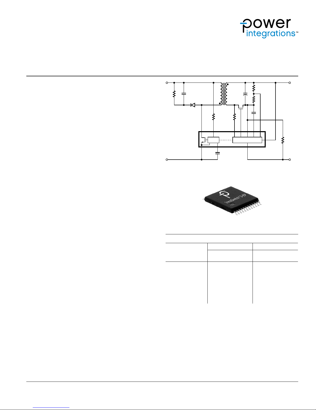
InnoSwitch3-EP
Primary FET
and Controller
Figure 1. Typical Application Schematic.
Figure 2. High Creepage, Safety-Compliant InSOP-24D Package.
Output Power Table
Product
INN3672C 12 W 10 W
INN3673C 15 W 12 W
INN3 674C 25 W 20 W
INN3675C 30 W 25 W
INN3676C 40 W 36 W
INN3677C 45 W 40 W
Table 1. Output Power Table.
Notes:
1. Minimum continuous power in a typical non-ventilated enclosed typical size
adapter measured at 40 °C ambient. Max output power is dependent on the
design. With condition that package temperature must be < 125 °C.
2. Minimum peak power capability.
3. Package: InSOP-24D.
D V
S IS
3
SR FET
GND
BPS
FB
VOUT
Secondary
Control IC
PI-8184-050217
BPP
FWD
SR
230 VAC ± 15% 85-265 VAC
Peak or
Open Frame
1,2
Peak or
Open Frame
Optional
Current
Sense
1,2
www.power.com August 2018
This Product is Covered by Patents and/or Pending Patent Applications.
Page 2
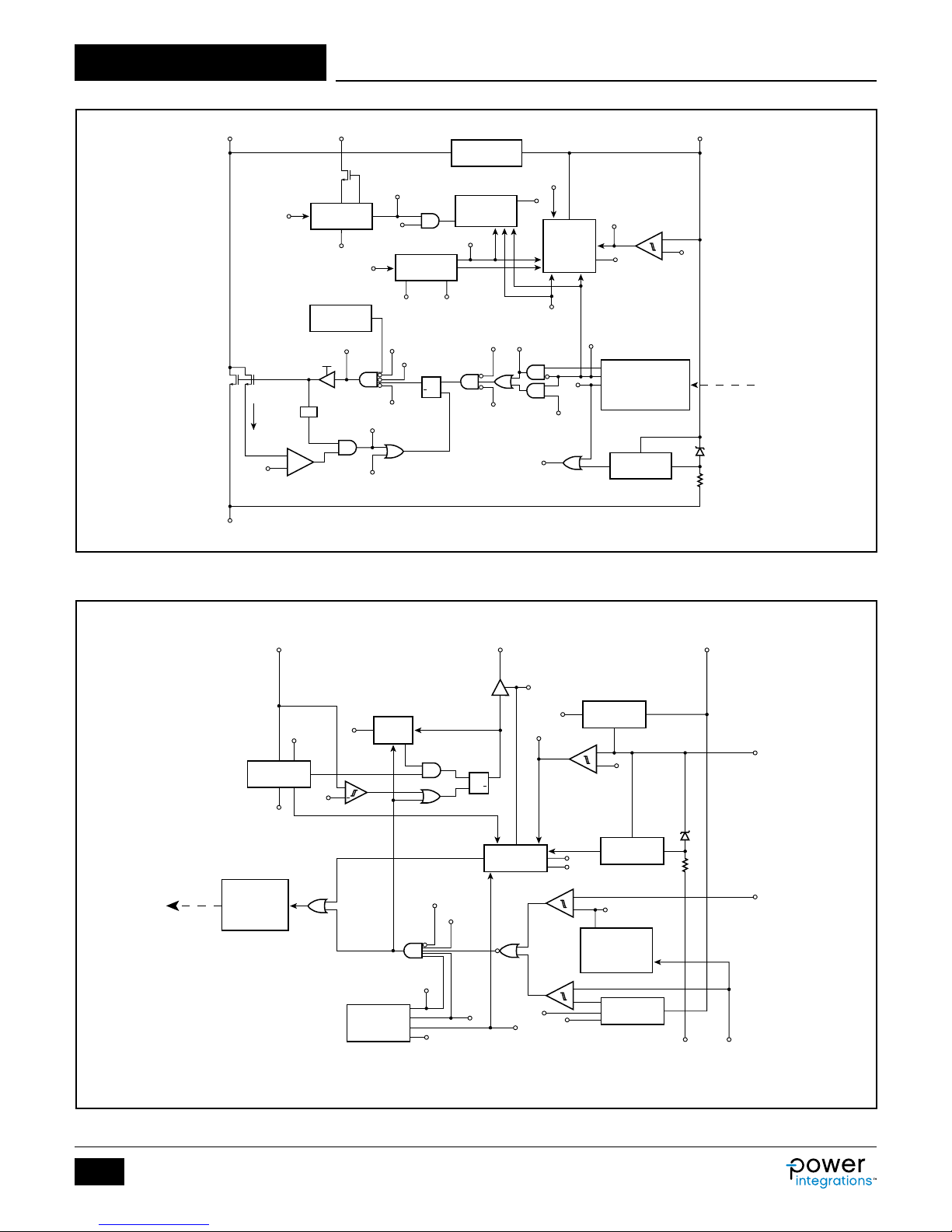
InnoSwitch3-EP
PI-8045d-091217
DETECTOR
ENABLE
SR
FORWARD
(FWD)
FEEDBACK
(FB)
SECONDARY
BYPASS
(BPS)
SECONDARY
GROUND
(GND)
ISENSE
(IS)
To
Primary
Receiver
SYNCRONOUS RECTIFIER DRIVE
(SR)
FEEDBACK
COMPENSATION
FEEDBACK
DRIVER
INH
QR
Ts
MAX
INH
QR
t
OFF(MIN)
t
SECINH(MAX)
t
SS(RAMP)
4.4 V
3.9 V
SR CONTROL
INH
DCM
VREF
IS THRESHOLD
V
PK
FORWARD
BPS
UV
OUTPUT VOLTAGE
(VOUT)
OSCILLATOR/
TIMER
REGULATOR
4.4 V
SECONDARY
LATCH
CONSTANT
POWER
HANDSHAKE/
LATCH-OFF
SR
THRESHOLD
CONTROL
SQQ
R
+
+
-
+
-
+
-
VOUT
DRAIN
(D)
GATE
SOURCE
(S)
SenseFET
I
S
V
ILIM
Power
MOSFET
Figure 3. Primary Controller Block Diagram.
UNDER/OVER
INPUT VOLTAGE (V)
INTERFACE
THERMAL
SHUTDOWN
BPP
DRIVER
LEB
+
-
LINE
UV/OV
GATE
GATE
ILIM
t
ON(MAX)
PRIMARY BYPASS
REGULATOR
ENABLE
BPP/UV
OSCILLATOR/
TIMERS
t
ON(MAX)tOFF(BLOCK)
OV/UV
AUTO-RESTART
COUNTER
RESET
PRIM-CLK
JITTER
FAULT
FAULT
SecREQ
ENABLE
PRIMARY
BYPASS PIN
CAPACITOR
SELECT AND
CURRENT
LIMIT
GATE
LATCH-OFF
QRS
BPP/UV
Q
t
OFF(BLOCK)
PRIM-CLK
SEC-
LATCH
LATCH-OFF
BPP/UV
V
ILIM
PRIM/SEC
SecPulse
PRIM/SEC
PRIMARY OVP
PRIMARY BYPASS
PRIMARY
BYPASS PIN
UNDERVOLTAGE
+
-
V
RECEIVER
CONTROLLER
LATCH
PI-8044-083017
SHUNT
V
(BPP)
BP+
From
Secondary
Controller
Figure 4. Secondary Controller Block Diagram.
2
Rev. D 08/18
www.power.com
Page 3
Pin Functional Description
ISENSE (IS) Pin (Pin 1)
Connection to the power supply output terminals. An external
current sense resistor should be connected between this and the
GND pin. If current regulation is not required, this pin should be tied
to the GND pin.
SECONDARY GROUND (GND) (Pin 2)
GND for the secondary IC. Note this is not the power supply output
GND due to the presence of the sense resistor between this and the
ISENSE pin.
FEEDBACK (FB) Pin (Pin 3)
Connection to an external resistor divider to set the power supply
output voltage.
SECONDARY BYPASS (BPS) Pin (Pin 4)
Connection point for an external bypass capacitor for the secondary
IC supply.
SYNCHRONOUS RECTIFIER DRIVE (SR) Pin (Pin 5)
Gate driver for external SR FET. If no SR FET is used connect this pin
to GND.
OUTPUT VOLTAGE (VOUT) Pin (Pin 6)
Connected directly to the output voltage, to provide current for the
controller on the secondary-side and provide secondary protection.
FORWARD (FWD) Pin (Pin 7)
The connection point to the switching node of the transformer output
winding providing information on primary switch timing. Provides power
for the secondary-side controller when V
NC Pin (Pin 8-12)
Leave open. Should not be connected to any other pins.
UNDER/OVER INPUT VOLTAGE (V) Pin (Pin 13)
A high-voltage pin connected to the AC or DC side of the input bridge
for detecting undervoltage and overvoltage conditions at the power
supply input. This pin should be tied to SOURCE pin to disable UV/OV
protection.
PRIMARY BYPASS (BPP) Pin (Pin 14)
The connection point for an external bypass capacitor for the
primary-side supply. This is also the ILIM selection pin for choosing
standard ILIM or ILIM+1.
NC Pin (Pin 15)
Leave open. Should not be connected to any other pins.
SOURCE (S) Pin (Pin 16-19)
These pins are the power MOSFET source connection. Also ground
reference for primary BYPASS pin.
DRAIN (D) Pin (Pin 24)
Power MOSFET drain connection.
is below threshold.
OUT
InnoSwitch3-EP
V 13 12 NC
BPP 14 11 NC
NC 15 10 NC
S 16-19
D 24
Figure 5. Pin Conguration.
InnoSwitch3-EP Functional Description
The InnoSwitch3-EP combines a high-voltage power MOSFET switch,
along with both primary-side and secondary-side controllers in one
device.
The architecture incorporates a novel inductive coupling feedback
scheme (FluxLink) using the package lead frame and bond wires to
provide a safe, reliable, and cost-effective means to transmit
accurate, output voltage and current information from the secondary
controller to the primary controller.
The primary controller on InnoSwitch3-EP is a Quasi-Resonant (QR)
yback controller that has the ability to operate in continuous
conduction mode (CCM), boundary mode (CrM) and discontinuous
conduction mode (DCM). The controller uses both variable frequency
and variable current control schemes. The primary controller consists
of a frequency jitter oscillator, a receiver circuit magnetically coupled to
the secondary controller, a current limit controller, 5 V regulator on
the PRIMARY BYPASS pin, audible noise reduction engine for light
load operation, bypass overvoltage detection circuit, a lossless input
line sensing circuit, current limit selection circuitry, over-temperature
protection, leading edge blanking, secondary output diode / SR FET
short protection circuit and a 725 V power MOSFET.
The InnoSwitch3-EP secondary controller consists of a transmitter
circuit that is magnetically coupled to the primary receiver, a constant
voltage (CV) and a constant current (CC) control circuit, a 4.4 V
regulator on the SECONDARY BYPASS pin, synchronous rectier FET
driver, QR mode circuit, oscillator and timing circuit, and numerous
integrated protection features.
Figure 3 and Figure 4 show the functional block diagrams of the
primary and secondary controller, highlighting the most important
features.
9 NC
8 NC
7 FWD
6 VOUT
5 SR
4 BPS
3 FB
2 GND
1 IS
PI-7877-022216
www.power.com
3
Rev. D 08/18
Page 4
InnoSwitch3-EP
Primary Controller
InnoSwitch3-EP has variable frequency QR controller plus CCM/CrM/
DCM operation for enhanced efciency and extended output power
capability.
PRIMARY BYPASS Pin Regulator
The PRIMARY BYPASS pin has an internal regulator that charges the
PRIMARY BYPASS pin capacitor to V
DRAIN pin whenever the power MOSFET is off. The PRIMARY
BYPA SS pin is the internal supply voltage node. When the power
MOSFET is on, the device operates from the energy stored in the
PRIMARY BYPASS pin capacitor.
In addition, a shunt regulator clamps the PRIMARY BYPASS pin
voltage to V
pin through an external resistor. This allows the InnoSwitch3-EP to
when current is provided to the PRIMARY BYPASS
SHUNT
be powered externally through a bias winding, decreasing the no-load
consumption to less than 15 mW in a 5 V output design.
Primary Bypass ILIM Programming
InnoSwitch3-EP ICs allows the user to adjust current limit (ILIM)
settings through the selection of the PRIMARY BYPASS pin capacitor
value. A ceramic capacitor can be used.
There are 2 selectable capacitor sizes - 0.47 mF and 4.7 mF for setting
standard and increased ILIM settings respectively.
Primary Bypass Undervoltage Threshold
The PRIMARY BYPASS pin undervoltage circuitry disables the power
MOSFET when the PRIMARY BYPASS pin voltage drops below ~4.5 V
(V
- V
BPP
pin voltage falls below this threshold, it must rise to V
) in steady-state operation. Once the PRIMARY BYPASS
BP(H)
re-enable turn-on of the power MOSFET.
Primary Bypass Output Overvoltage Function
The PRIMARY BYPASS pin has a latching OV protection feature. A
Zener diode in parallel with the resistor in series with the PRIMARY
BYPASS pin capacitor is typically used to detect an overvoltage on the
primary bias winding and activate the protection mechanism. In the
event that the current into the PRIMARY BYPASS pin exceeds ISD, the
device will latch-off or disable the power MOSFET switching for a time
t
, after which time the controller will restart and attempt to
AR(O FF)
return to regulation (see Secondary Fault Response in the Feature
Code Addenda).
VOUT OV protection is also included as an integrated feature on the
secondary controller (see Output Voltage Protection).
Over-Temperature Protection
The thermal shutdown circuitry senses the primary MOSFET die
temperature. The threshold is set to T
latch-off response.
Hysteretic response: If the die temperature rises above the threshold,
the power MOSFET is disabled and remains disabled until the die
temperature falls by T
large amount of hysteresis is provided to prevent over-heating of the
at which point switching is re-enabled. A
SD(H)
PCB due to a continuous fault condition.
Latch-off response: If the die temperature rises above the threshold
the power MOSFET is disabled. The latching condition is reset by
bringing the PRIMARY BYPASS pin below V
the UNDER/OVER INPUT VOLTAGE pin UV (I
by drawing current from the
BPP
to
SHUNT
with either a hysteretic or
SD
or by going below
BPP(RESET)
) threshold.
UV-
1.05
1.0
(A)
0.95
LIM
0.9
0.85
Normalized I
0.8
0.75
30 40 50 60 70 90 10080
Steady-State Switching Frequency (kHz)
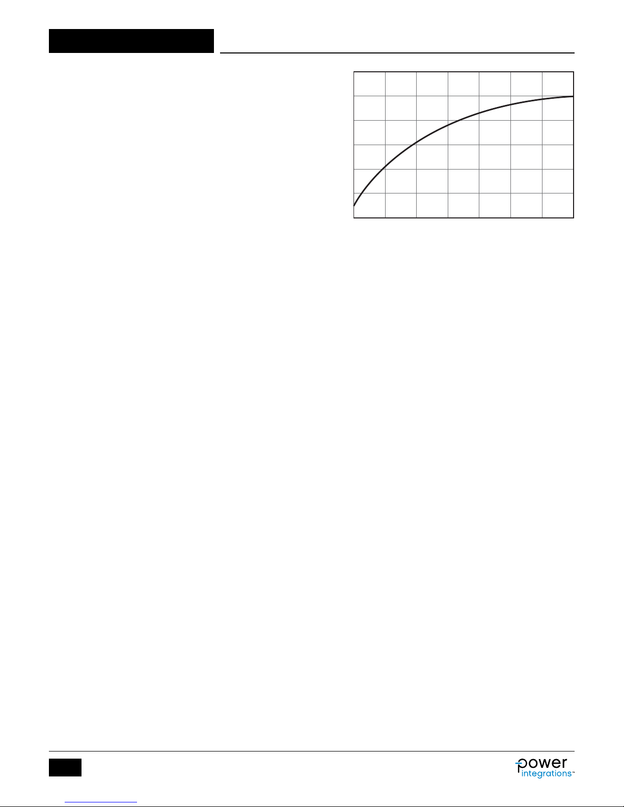
Figure 6. Normalized Primary Current vs. Frequency.
Current Limit Operation
The primary-side controller has a current limit threshold ramp that is
linearly decreasing to the time from the end of the previous primary
switching cycle (i.e. from the time the primary MOSFET turns off at
the end of a switching cycle).
This characteristic produces a primary current limit that increases as
the switching frequency (load) increases (Figure 6).
This algorithm enables the most efcient use of the primary switch
with the benet that this algorithm responds to digital feedback
information immediately when a feedback switching cycle request is
received.
At high load, switching cycles have a maximum current approaching
100% I
load decreases. Once 30% current limit is reached, there is no
. This gradually reduces to 30% of the full current limit as
LIM
further reduction in current limit (since this is low enough to avoid
audible noise). The time between switching cycles will continue to
increase as load reduces.
Jitter
The normalized current limit is modulated between 100% and 95%
at a modulation frequency of f
~7 kHz with average frequency of ~100 kHz.
. This results in a frequency jitter of
M
Auto-Restart
In the event a fault condition occurs (such as an output overload,
output short-circuit, or external component/pin fault), the
InnoSwitch3-EP enters auto-restart (AR) or latches off. The latching
condition is reset by bringing the PRIMARY BYPASS pin below ~3 V or
by going below the UNDER/OVER INPUT VOLTAGE pin UV (I
threshold.
In auto-restart, switching of the power MOSFET is disabled for t
There are 2 ways to enter auto-restart:
)
UV-
AR(O FF)
1. Continuous secondary requests at above the overload detection
frequency f
2. No requests for switching cycles from the secondary for >t
The second is included to ensure that if communication is lost, the
primary tries to restart. Although this should never be the case in
normal operation, it can be useful when system ESD events (for
example) causes a loss of communication due to noise disturbing the
secondary controller. The issue is resolved when the primary restarts
after an auto-restart off-time.
(~110 kHz) for longer than 82 ms (tAR).
OVL
AR(SK)
.
PI-8205-120516
.
4
Rev. D 08/18
www.power.com
Page 5
InnoSwitch3-EP
The rst auto-restart off-time is short (t
restart time is to provide quick recovery under fast reset conditions.
). This short auto-
AR(OFF)SH
The short auto-restart off-time allows the controller to quickly check to
determine whether the auto-restart condition is maintained beyond
t
. If so, it will resort to a full auto-restart off-time.
AR(OFF)SH
The auto-restart is reset as soon as an AC reset occurs.
SOA Protection
In the event that there are two consecutive cycles where the I
reached within ~500 ns (the blanking time + current limit delay time),
is
LIM
the controller will skip 2.5 cycles or ~25 ms (based on full frequency
of 100 kHz). This provides sufcient time for the transformer to reset
with large capacitive loads without extending the start-up time.
Secondary Rectier/SR MOSFET Short Protection (SRS)
In the event that the output diode or SR FET is short-circuited before
or during the primary conduction cycle, the drain current (prior to the
end of the leading edge blanking time) can be much higher than the
maximum current limit threshold. If the controller turns the highvoltage power MOSFET off, the resulting peak drain voltage could
exceed the rated BV
even with minimum on-time.
of the device, resulting in catastrophic failure
DSS
To address this issue, the controller features a circuit that reacts
when the drain current exceeds the maximum current limit threshold
prior to the end of leading-edge blanking time. If the leading-edge
current exceeds current limit within a cycle (200 ns), the primary
controller will trigger a 30 ms off-time event. SOA mode is triggered if
there are two consecutive cycles above current limit within t
(~500 ns). SRS mode also triggers ~200 ms off-time, if the current
LES
limit is reached within 200 ns after a 30 ms off-time.
Input Line Voltage Monitoring
The UNDER/OVER INPUT VOLTAGE pin is used for input undervoltage
and overvoltage sensing and protection.
A 4 MΩ resistor is tied between the high-voltage DC bulk capacitor
after the bridge (or to the AC side of the bridge rectier for fast AC
reset) and the UNDER/OVER INPUT VOLTAGE pin to enable this
functionality. This function can be disabled by shorting the UNDER/
OVER INPUT VOLTAGE pin to SOURCE pin.
At power-up, after the primary bypass capacitor is charged and the
ILIM state is latched, and prior to switching, the state of the UNDER/
OVER INPUT VOLTAGE pin is checked to conrm that it is above the
brown-in and below the overvoltage shutdown thresholds.
In normal operation, if the UNDER/OVER INPUT VOLTAGE pin current
falls below the brown-out threshold and remains below brown-in for
longer than t
resume once the UNDER/OVER INPUT VOLTAGE pin current is above
, the controller enters auto-restart. Switching will only
UV-
the brown-in threshold.
In the event that the UNDER/OVER INPUT VOLTAGE pin current is
above the overvoltage threshold, the controller will also enter
auto-restart. Again, switching will only resume once the UNDER/
OVER INPUT VOLTAGE pin current has returned to within its normal
operating range.
The input line UV/OV function makes use of an internal high-voltage
MOSFET on the UNDER/OVER INPUT VOLTAGE pin to reduce power
consumption. If the cycle off-time t
internal high-voltage MOSFET will disconnect the external 4 MΩ
is greater than 50 ms, the
OFF
resistor from the internal IC to eliminate current drawn through the
4 MΩ resistor. The line sensing function will activate again at the
beginning of the next switching cycle.
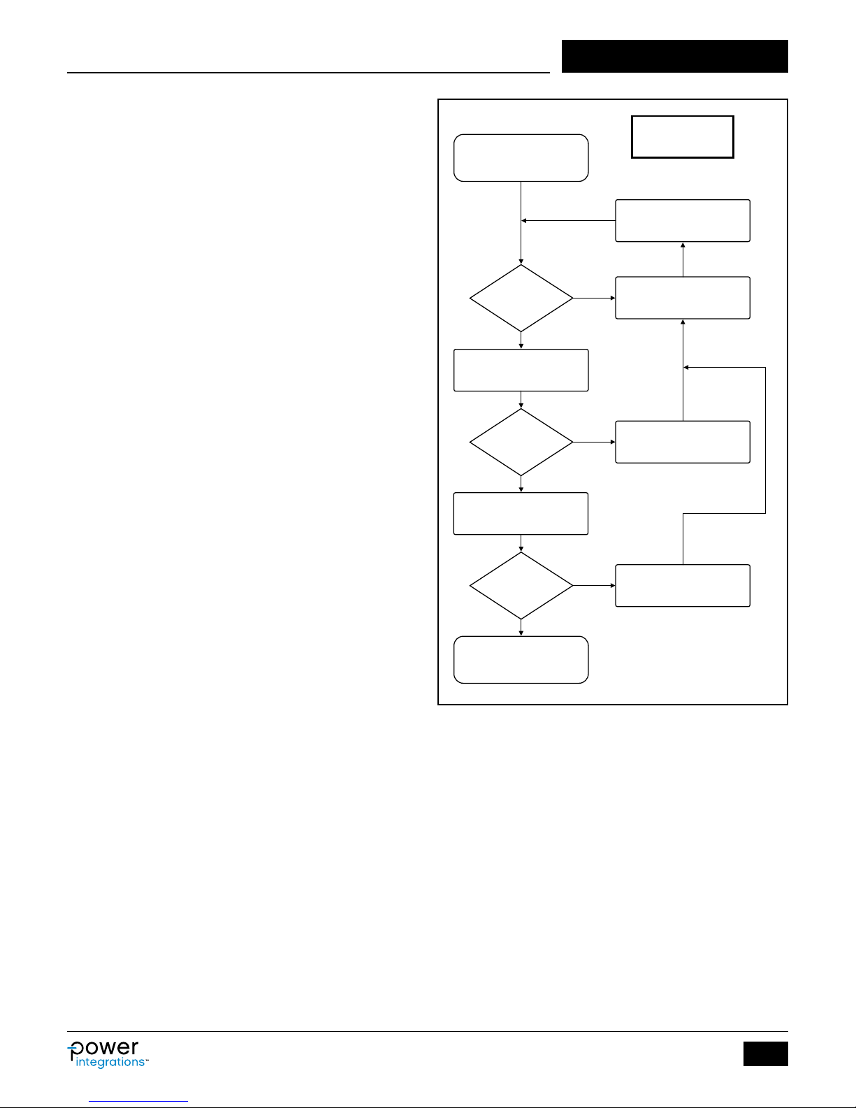
P: Primary Chip
Start
P: Powered Up, Switching
S: Powering Up
S: Has powered
up within 64 ms?
Yes
P: Switching
S: Sends Handshaking Pulses
P: Has Received
Handshaking
Pulses
Yes
P: Stops Switching, Hands
Over Control to Secondary
S: Has Taken
Control?
Yes
End of Handshaking,
Secondary Control Mode
Figure 7. Primary-Secondary Handshake Flowchart.
No
No
No
S: Secondary Chip
P: Auto-Restart
S: Powering Up
2s
P: Goes to Auto-Restart Off
S: Bypass Discharging
64 ms
P: Continuous Switching
S: Doesn’t Take Control
P: Not Switching
S: Doesn’t Take Control
PI-7416-102814
Primary-Secondary Handshake
At start-up, the primary-side initially switches without any feedback
information (this is very similar to the operation of a standard
TOPSwitch™, TinySwitch™ or LinkSwitch™ controllers).
If no feedback signals are received during the auto-restart on-time
(t
), the primary goes into auto-restart mode. Under normal
AR
conditions, the secondary controller will power-up via the FORWARD
pin or from the OUTPUT VOLTAGE pin and take over control. From
this point onwards the secondary controls switching.
If the primary controller stops switching or does not respond to cycle
requests from the secondary during normal operation (when the
secondary has control), the handshake protocol is initiated to ensure
that the secondary is ready to assume control once the primary
begins to switch again. An additional handshake is also triggered if
the secondary detects that the primary is providing more cycles than
were requested.
www.power.com
5
Rev. D 08/18
Page 6

InnoSwitch3-EP
The most likely event that could require an additional handshake is
when the primary stops switching as the result of a momentary line
brown-out event. When the primary resumes operation, it will default
to a start-up condition and attempt to detect handshake pulses from
the secondary.
If the secondary does not detect that the primary responds to
switching requests for 8 consecutive cycles, or if the secondary
detects that the primary is switching without cycle requests for 4 or
more consecutive cycles, the secondary controller will initiate a
second handshake sequence. This provides additional protection
against cross-conduction of the SR FET while the primary is
switching. This protection mode also prevents an output overvoltage
condition in the event that the primary is reset while the secondary is
still in control.
Wait and Listen
When the primary resumes switching after initial power-up recovery
from an input line voltage fault (UV or OV) or an auto-restart event, it
will assume control and require a successful handshake to relinquish
control to the secondary controller.
As an additional safety measure the primary will pause for an
auto-restart on-time period, t
this “wait” time, the primary will “listen” for secondary requests. If it
(~82 ms), before switching. During
AR
sees two consecutive secondary requests, separated by ~30 ms, the
primary will infer secondary control and begin switching in slave
mode. If no pulses occurs during the tAR “wait” period, the primary
will begin switching under primary control until handshake pulses are
received.
Audible Noise Reduction Engine
The InnoSwitch3-EP features an active audible noise reduction mode
whereby the controller (via a “frequency skipping” mode of operation)
avoids the resonant band (where the mechanical structure of the
power supply is most likely to resonate − increasing noise amplitude)
between 7 kHz and 12 kHz - 143 ms and 83 ms. If a secondary
controller switch request occurs within this time window from the last
conduction cycle, the gate drive to the power MOSFET is inhibited.
Secondary Controller
As shown in the block diagram in Figure 4, the IC is powered by a
4.4 V (V
SECONDARY BYPASS pin is connected to an external decoupling
capacitor and fed internally from the regulator block.
The FORWARD pin also connects to the negative edge detection
block used for both handshaking and timing to turn on the SR FET
connected to the SYNCHRONOUS RECTIFIER DRIVE pin. The
FORWARD pin voltage is used to determine when to turn off the
SR FET in discontinuous conduction mode operation. This is when
the voltage across the R
In continuous conduction mode (CCM) the SR FET is turned off when
the feedback pulse is sent to the primary to demand the next
switching cycle, providing excellent synchronous operation, free of
any overlap for the FET turn-off.
The mid-point of an external resistor divider network between the
OUTPUT VOLTAGE and SECONDARY GROUND pins is tied to the
FEEDBACK pin to regulate the output voltage. The internal voltage
comparator reference voltage is VFB (1.265 V).
The external current sense resistor connected between ISENSE and
SECONDARY GROUND pins is used to regulate the output current in
constant current regulation mode.
) regulator which is supplied by either VOUT or FWD. The
BPS
of the SR FET drops below zero volts.
DS(O N)
Minimum Off-Time
The secondary controller initiates a cycle request using the inductiveconnection to the primary. The maximum frequency of secondarycycle requests is limited by a minimum cycle off-time of t
is in order to ensure that there is sufcient reset time after primary
OFF(MIN)
. This
conduction to deliver energy to the load.
Maximum Switching Frequency
The maximum switch-request frequency of the secondary controller
is f
.
SREQ
Frequency Soft-Start
At start-up the primary controller is limited to a maximum switching
frequency of f
at the switch-request frequency of 100 kHz.
and 75% of the maximum programmed current limit
SW
The secondary controller temporarily inhibits the FEEDBACK short
protection threshold (V
time. After hand-shake is completed the secondary controller linearly
ramps up the switching frequency from fSW to f
time period.
) until the end of the soft-start (t
FB(OFF)
SREQ
over the t
SS(R AMP)
SS(R AMP)
)
In the event of a short-circuit or overload at start-up, the device will
move directly into CC (constant-current) mode. The device will go
into auto-restart (AR), if the output voltage does not rise above the
V
threshold before the expiration of the soft-start timer (t
FB(AR)
after handshake has occurred.
SS(R AMP)
)
The secondary controller enables the FEEDBACK pin-short protection
mode (V
short maintains the FEEDBACK pin below the short-circuit threshold,
) at the end of the t
FB(OFF)
time period. If the output
SS(R AMP)
the secondary will stop requesting pulses triggering an auto-restart
cycle.
If the output voltage reaches regulation within the t
period, the frequency ramp is immediately aborted and the secondary
SS(R AMP)
time
controller is permitted to go full frequency. This will allow the
controller to maintain regulation in the event of a sudden transient
loading soon after regulation is achieved. The frequency ramp will
only be aborted if quasi-resonant-detection programming has already
occurred.
Maximum Secondary Inhibit Period
Secondary requests to initiate primary switching are inhibited to
maintain operation below maximum frequency and ensure minimum
off-time. Besides these constraints, secondary-cycle requests are
also inhibited during the “ON” time cycle of the primary switch (time
between the cycle request and detection of FORWARD pin falling
edge). The maximum time-out in the event that a FORWARD pin
falling edge is not detected after a cycle requested is ~30 ms.
Output Voltage Protection
In the event that the sensed voltage on the FEEDBACK pin is 2%
higher than the regulation threshold, a bleed current of ~2.5 mA (3
mA max) is applied on the OUTPUT VOLTAGE pin (weak bleed). This
bleed current increases to ~200 mA (strong bleed) in the event that
the FEEDBACK pin voltage is raised beyond ~10% of the internal
FEEDBACK pin reference voltage. The current sink on the OUTPUT
VOLTAGE pin is intended to discharge the output voltage after
momentary overshoot events. The secondary does not relinquish
control to the primary during this mode of operation.
If the voltage on the FEEDBACK pin is sensed to be 20% higher than
the regulation threshold, a command is sent to the primary to either
latch-off or begin an auto-restart sequence (see Secondary Fault
Response in Feature Code Addendum). This integrated V
be used independently from the primary sensed OVP or in conjunction.
OVP can
OUT
6
Rev. D 08/18
www.power.com
Page 7
InnoSwitch3-EP
Output Voltage
Request Window
Primary VDS
FEEDBACK Pin Short Detection
If the sensed FEEDBACK pin voltage is below V
secondary controller will complete the handshake to take control of
the primary complete t
auto-restart (no cycle requests made to primary for longer than t
and will stop requesting cycles to initiate
SS(R AMP)
second triggers auto-restart).
at start-up, the
FB(OFF)
AR(S K)
During normal operation, the secondary will stop requesting pulses
from the primary to initiate an auto-restart cycle when the FEEDBACK
pin voltage falls below the V
protection mode is on for less than ~10 ms. By this mechanism, the
threshold. The deglitch lter on the
FB(OFF)
secondary will relinquish control after detecting that the FEEDBACK
pin is shorted to ground.
Auto-Restart Thresholds
The OUTPUT VOLTAGE pin includes a comparator to detect when the
output voltage falls below V
t
or t
FB(AR)
control when this fault condition is detected. This threshold is meant
respectively. The secondary controller will relinquish
VO(AR)
FB(AR)
or V
, for a duration exceeding
VO(AR)
to limit the range of constant current (CC) operation and is included
to support high power charger applications.
SECONDARY BYPASS Pin Overvoltage Protection
The InnoSwitch3-EP secondary controller features a SECONDARY
BYPASS pin OV feature similar to the PRIMARY BYPASS pin OV
feature. When the secondary is in control, in the event that the
SECONDARY BYPASS pin current exceeds I
secondary will send a command to the primary to initiate an
auto-restart off-time (t
AR(O FF)
).
(~7 mA) the
BPS (SD)
Output Constant Current and Constant Power Regulation
The InnoSwitch3-EP regulates the output current through an external
current sense resistor between the ISENSE and SECONDARY
GROUND pins and also controls output power in conjunction with the
output voltage sensed on the OUTPUT VOLTAGE pin. If constant
current regulation is not required, the ISENSE pin must be tied to the
SECONDARY GROUND pin. The InnoSwitch3-EP has constant current
regulation below the V
prole above the VPK threshold. The transition between CP and CC is
threshold, and a constant output power
PK
set by the VPK threshold and the set constant current is programmed
by the resistor between the ISENSE and SECONDARY GROUND pins.
PI-8147-102816
FORWARD Pin Voltage
Figure 8. Intelligent Quasi-Resonant Mode Switching.
Time
Time
www.power.com
7
Rev. D 08/18
Page 8

InnoSwitch3-EP
SR Disable Protection
In each cycle SR is only engaged if a set cycle was requested by the
secondary controller and the negative edge is detected on the
FORWARD pin. In the event that the voltage on the ISENSE pin
exceeds approximately 3 times the CC threshold, the SR FET drive is
disabled until the surge current has diminished to nominal levels.
SR Static Pull-Down
To ensure that the SR gate is held low when the secondary is not in
control, the SYNCHRONOUS RECTIFIER DRIVE pin has a nominally
“ON” device to pull the pin low and reduce any voltage on the SR gate
due to capacitive coupling from the FORWARD pin.
Open SR Protection
In order to protect against an open SYNCHRONOUS RECTIFIER
DRIVE pin system fault the secondary controller has a protection
mode to ensure the SYNCHRONOUS RECTIFIER DRIVE pin is
connected to an external FET. If the external capacitance on the
SYNCHRONOUS RECTIFIER DRIVE pin is below 100 pF, the device
will assume the SYNCHRONOUS RECTIFIER DRIVE pin is “open” and
there is no FET to drive. If the pin capacitance detected is above
100 pF, the controller will assume an SR FET is connected.
In the event the SYNCHRONOUS RECTIFIER DRIVE pin is detected to
be open, the secondary controller will stop requesting pulses from
the primary to initiate auto-restart.
If the SYNCHRONOUS RECTIFIER DRIVE pin is tied to ground at
start-up, the SR drive function is disabled and the open
SYNCHRONOUS RECTIFIER DRIVE pin protection mode is also
disabled.
Intelligent Quasi-Resonant Mode Switching
In order to improve conversion efciency and reduce switching
losses, the InnoSwitch3-EP features a means to force switching when
the voltage across the primary switch is near its minimum voltage
when the converter operates in discontinuous conduction mode (DCM).
This mode of operation is automatically engaged in DCM and disabled
once the converter moves to continuous-conduction mode (CCM).
Rather than detecting the magnetizing ring valley on the primaryside, the peak voltage of the FORWARD pin voltage as it rises above
the output voltage level is used to gate secondary requests to initiate
the switch “ON” cycle in the primary controller.
The secondary controller detects when the controller enters in
discontinuous-mode and opens secondary cycle request windows
corresponding to minimum switching voltage across the primary
power MOSFET.
Quasi-Resonant (QR) mode is enabled for 20 ms after DCM is detected
or when ring amplitude (pk-pk) >2 V. Afterwards, QR switching is
disabled, at which point switching may occur at any time a secondary
request is initiated.
The secondary controller includes blanking of ~1 ms to prevent false
detection of primary “ON” cycle when the FORWARD pin rings below
ground. See Figure 8.
8
Rev. D 08/18
www.power.com
Page 9
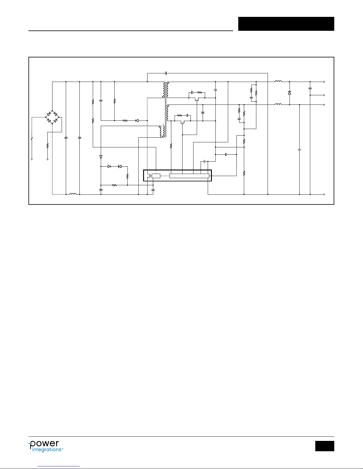
Applications Example
PI-8374-051818
C10
R3
2 MΩ
10 µF
400 V
L1
330 µH
1%
R4
1.8 MΩ
1%
C3
DFLR1200-7
BR1
DF08S
800 V
F1
1 A
RT1
10 Ω
90 - 265
VAC
L N
C2
10 µF
400 V
O
t
InnoSwitch3-EP
470 pF
250 VAC
21FL1
CONTROL
BPP
4.7 µF
4
3
C6
16 V
FL2
6
5
NC
T1
EE1621
InnoSwitch3-EP
INN3672C-H602
R9
47 Ω
1/10 W
FWD
R24
62 Ω
1/8 W
U1
C4
R8
1000 pF
200 kΩ
630 V
D1
R22
DFLR1600-7
68 Ω
600 V
D7
C5
22 µF
50 V
MMSZ5231B-7-F
D3
BAV21WS-7-F
6.2 kΩ
1/10 W
VR1
D V
R26
36 Ω
R6
1/10 W
S IS
AO4486
C22
1 nF
200 V
Q1
AO6420
SR
C21
1 nF
200 V
Q2
30 Ω
1/8 W
VO
R25
2.2 µF
C19
680 µF
16 V
C18
560 µF
6.3 V
C7
25 V
BPS
C8
330 pF
50 V
GND
FB
R29
100 Ω
1/10 W
C23
2.2 nF
50 V
R30
100 Ω
1/10 W
C24
2.2 nF
50 V
R16
133 kΩ
1%
1/16 W
R13
33.2 kΩ
1%
1/16 W
R12
0.2 Ω
1%
R27
1.2 MΩ
1%
1/16 W
10 µH
10 µH
L2
L3
VR2
SMAZ8V2-13-F
8.2 V
C12
2.2 µF
25 V
C14
2.2 µF
25 V
12 V, 0.7 A
12 V
RTN
5 V, 0.3 A
RTN
Figure 9. Schematic DER-611, 5 V, 0.3 A and 12 V, 0.7 A for HVAC (Heating, Ventilation and Air-Conditioning) Application.
The circuit shown in Figure 9 is a low cost 5 V, 0.3 A and 12 V, 0.7 A
dual output power supply using INN3672C. This dual output design
features high efcient design satisfying cross regulation requirement
without a post-regulator.
Bridge rectier BR1 recties the AC input supply. Capacitors C2 and
C3 provide ltering of the rectied AC input and together with
inductor L1 form a pi-lter to attenuate differential mode EMI.
Y capacitor C10 connected between the power supply output and
input help reduce common mode EMI.
Thermistor RT1 limits the inrush current when the power supply is
connected to the input AC supply.
Input fuse F1 provides protection against excess input current
resulting from catastrophic failure of any of the components in the
power supply. One end of the transformer primary is connected to
the rectied DC bus; the other is connected to the drain terminal of
the MOSFET inside the InnoSwitch3-EP IC (U1).
A low-cost RCD clamp formed by diode D1, resistors R22, R8, and
capacitor C4 limits the peak drain voltage of U1 at the instant of
turn-off of the MOSFET inside U1. The clamp helps to dissipate the
energy stored in the leakage reactance of transformer T1.
The InnoSwitch3-EP IC is self-starting, using an internal high-voltage
current source to charge the PRIMARY BYPASS pin capacitor (C6)
when AC is rst applied. During normal operation the primary-side
block is powered from an auxiliary winding on the transformer T1.
Output of the auxiliary (or bias) winding is rectied using diode D7
and ltered using capacitor C5. Resistor R6 limits the current being
supplied to the PRIMARY BYPASS pin of InnoSwitch3-EP IC (U1). The
latch off primary-side overvoltage protection is obtained using Zener
diode VR1 with current limiting resistor R26.
The secondary-side controller of the InnoSwitch3-EP IC provides
output voltage sensing, output current sensing and drive to a
MOSFET providing synchronous rectication. The 5 V secondary of
the transformer is rectied by SR FET Q1 and ltered by capacitor
C18. High frequency ringing during switching transients that would
otherwise create radiated EMI is reduced via a snubber (resistor R24
and capacitor C22). The 12 V secondary of the transformer is rectied
by SR FET Q2 and ltered by capacitor C19. High frequency ringing
during switching transients that would otherwise create radiated EMI
is reduced via a snubber (resistor R25 and capacitor C21).
Synchronous rectications (SR) are provided by MOSFETs Q1 and Q2.
Q1 and Q2 are turned on by the secondary-side controller inside IC
U1, based on the winding voltage sensed via resistor R9 and fed into
the FORWARD pin of the IC.
In continuous conduction mode of operation, the MOSFET is turned
off just prior to the secondary-side’s commanding a new switching
cycle from the primary. In discontinuous conduction mode of
operation, the power MOSFET is turned off when the voltage drop
across the MOSFET falls below 0 V. Secondary-side control of the
primary-side power MOSFET avoids any possibility of cross
conduction of the two MOSFETs and provides extremely reliable
synchronous rectication.
The secondary-side of the IC is self-powered from either the
secondary winding forward voltage or the output voltage. Capacitor
C7 connected to the SECONDARY BYPASS pin of InnoSwitch3-EP IC
U1, provides decoupling for the internal circuitry.
Total output current is sensed by R12 between the IS and GROUND
pins with a threshold of approximately 35 mV to reduce losses. Once
the current sense threshold is exceeded the device adjusts the
number of switch pulses to maintain a xed output current.
The output voltages are sensed via resistor divider R13, R16, and
R27, and output voltages are regulated so as to achieve a voltage of
1.265 V on the FEEDBACK pin. The 12 V phase boost circuit, R30 and
C24, in parallel with 12 V feedback resistor, R27, and 5 V phase boost
circuit, R29 and C23, in parallel with 5 V feedback resistor, R16,
reduce the output voltage ripples. Capacitor C8 provides noise
www.power.com
9
Rev. D 08/18
Page 10

InnoSwitch3-EP
ltering of the signal at the FEEDBACK pin. Zener VR2 was added for
tighter cross-regulation to limit the 12 V output when it is unloaded.
Resistors R3 and R4 provide line voltage sensing and provide a current
to U1, which is proportional to the DC voltage across capacitor C3. At
approximately 100 VDC, the current through these resistors exceeds
the line undervoltage threshold, which results in enabling of U1. At
approximately 435 VDC, the current through these resistors exceeds
the line over voltage threshold, which results in disabling of U1.
Key Application Considerations
Output Power Table
The data sheet output power table (Table 1) represents the maximum
practical continuous output power level that can be obtained under
the following conditions:
1. The minimum DC input voltage is 90 V or higher for 85 VAC input,
220 V or higher for 230 VAC input or 115 VAC with a voltagedoubler. Input capacitor voltage should be sized to meet these
criteria for AC input designs.
2. Efciency assumptions depend on power level. Smallest device
power level assumes efciency >84% increasing to >89% for the
largest device.
3. Transformer primary inductance tolerance of ±10%.
4. Reected output voltage (VOR) is set to maintain K
minimum input voltage for universal line and KP = 1 for high input
line designs.
5. Maximum conduction losses for adapters is limited to 0.6 W, 0.8 W
for open frame designs.
6. Increased current limit is selected for peak and open frame power
columns and standard current limit for adapter columns.
7. The part is board mounted with SOURCE pins soldered to a
sufcient area of copper and/or a heat sink to keep the SOURCE
pin temperature at or below 110 °C.
8. Ambient temperature of 50 °C for open frame designs and 40 °C
for sealed adapters.
9. Below a value of 1, K
current. To prevent reduced power delivery, due to premature
termination of switching cycles, a transient KP limit of ≥0.25 is
recommended. This prevents the initial current limit (I
being exceeded at MOSFET turn-on.
Primary-Side Overvoltage Protection (Latch-Off Mode)
Primary-side output overvoltage protection provided by the
InnoSwitch3-EP IC uses an internal latch that is triggered by a
threshold current of I
an internal lter, the PRIMARY BYPASS pin capacitor forms an
external lter helping noise immunity. For the bypass capacitor to be
effective as a high frequency lter, the capacitor should be located as
close as possible to the SOURCE and PRIMARY BYPASS pins of the
device.
The primary sensed OVP function can be realized by connecting a
series combination of a Zener diode, a resistor and a blocking diode
from the rectied and ltered bias winding voltage supply to the
PRIMARY BYPASS pin. The rectied and ltered bias winding output
voltage may be higher than expected (up to 1.5X or 2X the desired
value) due to poor coupling of the bias winding with the output
winding and the resulting ringing on the bias winding voltage
waveform. It is therefore recommended that the rectied bias
winding voltage be measured. This measurement should be ideally
done at the lowest input voltage and with highest load on the output.
This measured voltage should be used to select the components
is the ratio of ripple to peak primary
P
into the PRIMARY BYPASS pin. In addition to
SD
= 0.8 at
P
) from
INT
required to achieve primary sensed OVP. It is recommended that a
Zener diode with a clamping voltage approximately 6 V lower than the
bias winding rectied voltage at which OVP is expected to be
triggered be selected. A forward voltage drop of 1 V can be assumed
for the blocking diode. A small signal standard recovery diode is
recommended. The blocking diode prevents any reverse current
discharging the bias capacitor during start-up. Finally, the value of
the series resistor required can be calculated such that a current
higher than I
output overvoltage.
will ow into the PRIMARY BYPASS pin during an
SD
Reducing No-load Consumption
The InnoSwitch3-EP IC can start in self-powered mode, drawing
energy from the BYPASS pin capacitor charged through an internal
current source. Use of a bias winding is however required to provide
supply current to the PRIMARY BYPASS pin once the InnoSwitch3-EP
IC has started switching. An auxiliary (bias) winding provided on the
transformer serves this purpose. A bias winding driver supply to the
PRIMARY BYPASS pin enables design of power supplies with no-load
power consumption less than 15 mW. Resistor R6 shown in Figure 9
should be adjusted to achieve the lowest no-load input power.
Secondary-Side Overvoltage Protection (Auto-Restart Mode)
The secondary-side output overvoltage protection provided by the
InnoSwitch3-EP IC uses an internal auto restart circuit that is
triggered by an input current exceeding a threshold of I
SECONDARY BYPASS pin. The direct output sensed OVP function can
BPS (SD)
into the
be realized by connecting a Zener diode from the output to the
SECONDARY BYPASS pin. The Zener diode voltage needs to be the
difference between 1.25 × V
pin voltage. It is necessary to add a low value resistor in series with
and 4.4 V − the SECONDARY BYPASS
OUT
the OVP Zener diode to limit the maximum current into the
SECONDARY BYPASS pin.
Selection of Components
Components for InnoSwitch3-EP
Primary-Side Circuit
BPP Capacitor
A capacitor connected from the PRIMARY BYPASS pin of the
InnoSwitch3-EP IC to GND provides decoupling for the primary-side
controller and also selects current limit. A 0.47 mF or 4.7 mF capacitor
may be used. Though electrolytic capacitors can be used, often
surface mount multi-layer ceramic capacitors are preferred for use on
double sided boards as they enable placement of capacitors close to
the IC. Their small size also makes it ideal for compact power supplies.
16 V or 25 V rated X5R or X7R dielectric capacitors are recommended
to ensure that minimum capacitance requirements are met.
Bias Winding and External Bias Circuit
The internal regulator connected from the DRAIN pin of the MOSFET
to the PRIMARY BYPASS pin of the InnoSwitch3-EP primary-side
controller charges the capacitor connected to the PRIMARY BYPASS
pin to achieve start-up. A bias winding should be provided on the
transformer with a suitable rectier and lter capacitor to create a
bias supply that can be used to supply at least 1 mA of current to the
PRIMARY BYPASS pin.
The turns ratio for the bias winding should be selected such that 7 V
is developed across the bias winding at the lowest rated output
voltage of the power supply at the lowest load condition. If the
voltage is lower than this, no-load input power will increase.
10
Rev. D 08/18
www.power.com
Page 11

InnoSwitch3-EP
The bias current from the external circuit should be set to approximately
300 mA to achieve lowest no-load power consumption when operating
the power supply at 230 VAC input, (V
standard recovery rectier diode with low junction capacitance is
> 5 V). A glass passivated
BPP
recommended to avoid the snappy recovery typically seen with fast
or ultrafast diodes that can lead to higher radiated EMI.
An aluminum capacitor of at least 22 mF with a voltage rating 1.2
times greater than the highest voltage developed across the capacitor
is recommended. Highest voltage is typically developed across this
capacitor when the supply is operated at the highest rated output
voltage and load with the lowest input AC supply voltage.
Line UV and OV Protection
Resistors connected from the UNDER/OVER INPUT VOLTAGE pin to
the DC bus enable sensing of input voltage to provide line
undervoltage and overvoltage protection. For a typical universal
input application, a resistor value of 3.8 MΩ is recommended.
Figure 14 shows circuit congurations that enable either the line UV
or the line OV feature only to be enabled.
InnoSwitch3-EP features a primary sensed OV protection feature that
can be used to latch-off the power supply. Once the power supply is
latched off, it can be reset if the UNDER/OVER INPUT VOLTAGE pin
current is reduced to zero. Once the power supply is latched off,
even after the input supply is turned off, it can take considerable
amount of time to reset the InnoSwitch3-EP controller as the energy
stored in the DC bus will continue to provide current to the controller.
A fast AC reset can be achieved using the modied circuit
conguration shown in Figure 15. The voltage across capacitor C
reduces rapidly after input supply is disconnected reducing current
S
into the INPUT VOLTAGE MONITOR pin of the InnoSwitch3-EP IC and
resetting the InnoSwitch3-EP controller.
Primary Sensed OVP (Overvoltage Protection)
The voltage developed across the output of the bias winding tracks
the power supply output voltage. Though not precise, a reasonably
accurate detection of the amplitude of the output voltage can be
achieved by the primary-side controller using the bias winding
voltage. A Zener diode connected from the bias winding output to
the PRIMARY BYPASS pin can reliably detect a secondary overvoltage
fault and cause the primary-side controller to latch-off. It is
recommended that the highest voltage at the output of the bias
winding should be measured for normal steady-state conditions
(at full load and lowest input voltage) and also under transient load
conditions. A Zener diode rated for 1.25 times this measured voltage
will typically ensure that OVP protection will only operate in case of a
fault.
Primary-Side Snubber Clamp
A snubber circuit should be used on the primary-side as shown in
Figure 9. This prevents excess voltage spikes at the drain of the
MOSFET at the instant of turn-off of the MOSFET during each
switching cycle though conventional RCD clamps can be used. RCDZ
clamps offer the highest efciency. The circuit example shown in
Figure 9 uses an RCD clamp with a resistor in series with the clamp
diode. This resistor dampens the ringing at the drain and also limits
the reverse current through the clamp diode during reverse recovery.
Standard recovery glass passivated diodes with low junction
capacitance are recommended as these enable partial energy
recovery from the clamp thereby improving efciency.
Components for InnoSwitch3-EP
Secondary-Side Circuit
SECONDARY BYPASS Pin – Decoupling Capacitor
A 2.2 mF, 25 V multi-layer ceramic capacitor should be used for
decoupling the SECONDARY BYPASS pin of the InnoSwitch3-EP IC.
Since the SECONDARY BYPASS Pin voltage needs to be 4.4 V earlier
than output voltage reaches the regulation voltage level, the
signicantly higher BPS capacitor value could lead to output voltage
overshoot during start-up. Values lower than 1.5 mF may not enough
capacitance, which can cause unpredictable operation. The capacitor
must be located adjacent to the IC pins. The 25 V rating is necessary
to guarantee the actual value in operation since the capacitance of
ceramic capacitors drops with applied voltage. 10 V rated capacitors
are not recommended for this reason. Capacitors with X5R or X7R
dielectrics should be used for best results.
FORWARD Pin Resistor
A 47 Ω, 5% resistor is recommended to ensure sufcient IC supply
current. A higher or lower resistor value should not be used as it can
affect device operation such as the timing of the synchronous rectier
drive. Figures 10, 11, 12 and 13 below show examples of unacceptable
and acceptable FORWARD pin voltage waveforms. V
voltage drop across the SR.
0 V
V
SR(TH)
V
D
Figure 10. Unacceptable FORWARD Pin Waveform After Handshake with
SR MOSFET Conduction During Flyback Cycle.
0 V
V
SR(TH)
V
D
is forward
D
PI-8392-051818
PI-8393-051818
www.power.com
Figure 11. Acceptable FORWARD Pin Waveform After Handshake with
SR MOSFET Conduction During Flyback Cycle.
11
Rev. D 08/18
Page 12

InnoSwitch3-EP
0 V
V
SR(TH)
V
D
t1t
2
Figure 12. Unacceptable FORWARD Pin Waveform before Handshake with Body
Diode Conduction During Flyback Cycle.
Note:
If t1 + t2 = 1.5 ms ± 50 ns, the controller may fail the handshake and
trigger a primary bias winding OVP latch-off.
0 V
V
SR(TH)
V
D
Figure 13 Acceptable FORWARD Pin Waveform before Handshake with Body
Diode Conduction During Flyback Cycle.
SR MOSFET Operation and Selection
Although a simple diode rectier and lter works for the output, use
of an SR FET enables the signicant improvement in operating
efciency often necessary to meet the European CoC and the U.S.
DoE energy efciency requirements. The secondary-side controller
turns on the SR FET once the yback cycle begins. The SR FET gate
should be tied directly to the SYNCHRONOUS RECTIFIER DRIVE pin
of the InnoSwitch3-EP IC (no additional resistors should be connected
in the gate circuit of the SR FET). The SR FET is turned off once the
VDS of the SR FET reaches 0 V.
A FET with 18 mΩ R
FET with 8 mΩ R
output. The SR FET driver uses the SECONDARY BYPASS pin for its
is appropriate for a 5 V, 2 A output, and a
DS(O N)
is suitable for designs rated with a 12 V, 3 A
DS(O N)
supply rail, and this voltage is typically 4.4 V. A FET with a high
threshold voltage is therefore not suitable; FETs with a threshold
PI-8394-051818
PI-8393-051818
voltage of 1.5 V to 2.5 V are ideal although MOSFETs with a threshold
voltage (absolute maximum) as high as 4 V may be used provided
their data sheets specify R
of 4.5 V.
across temperature for a gate voltage
DS(O N)
There is a slight delay between the commencement of the yback
cycle and the turn-on of the SR FET. During this time, the body diode
of the SR FET conducts. If an external parallel Schottky diode is
used, this current mostly ows through the Schottky diode. Once the
InnoSwitch3-EP IC detects end of the yback cycle, voltage across
SR FET R
is completed with the current commutating to the body diode of the
reaches 0 V, any remaining portion of the yback cycle
DS(O N)
SR FET or the external parallel Schottky diode. Use of the Schottky
diode parallel to the SR FET may provide higher efciency and
typically a 1 A surface mount Schottky diode is adequate. However,
the gains are modest. For a 5 V, 2 A design the external diode adds
~0.1% to full load efciency at 85 VAC and ~0.2% at 230 VAC.
The voltage rating of the Schottky diode and the SR FET should be at
least 1.4 times the expected peak inverse voltage (PIV) based on the
turns ratio used for the transformer. 60 V rated FETs and diodes are
suitable for most 5 V designs that use a V
FETs and diodes are suitable for 12 V designs.
< 60 V, and 100 V rated
OR
The interaction between the leakage reactance of the output
windings and the SR FET capacitance (C
voltage waveform at the instance of voltage reversal at the winding
) leads to ringing on the
OSS
due to primary MOSFET turn-on. This ringing can be suppressed
using an RC snubber connected across the SR FET. A snubber
resistor in the range of 10 Ω to 47 Ω may be used (higher resistance
values lead to noticeable drop in efciency). A capacitance value of
1 nF to 2.2 nF is adequate for most designs.
Output Capacitor
Low ESR aluminum electrolytic capacitors are suitable for use with
most high frequency yback switching power supplies, though the
use of aluminum-polymer solid capacitors have gained considerable
popularity due to their compact size, stable temperature characteristics,
extremely low ESR and high RMS ripple current rating. These
capacitors enable the design of ultra-compact chargers and adapters.
Typically, 200 mF to 300 mF of aluminum-polymer capacitance per
ampere of output current is adequate. The other factor that
inuences choice of the capacitance is the output ripple. Ensure that
capacitors with a voltage rating higher than the highest output
voltage plus sufcient margin be used.
Output Voltage Feedback Circuit
The output voltage FEEDBACK pin voltage is 1.265 V [V
divider network should be connected at the output of the power
]. A voltage
FB
supply to divide the output voltage such that the voltage at the
FEEDBACK pin will be 1.265 V when the output is at its desired
voltage. The lower feedback divider resistor should be tied to the
SECONDARY GROUND pin. A 300 pF (or smaller) decoupling
capacitor should be connected at the FEEDBACK pin to the
SECONDARY GROUND pin of the InnoSwitch3-EP IC. This capacitor
should be placed close to the InnoSwitch3-EP IC.
12
Rev. D 08/18
www.power.com
Page 13

PI-8410-081717
+
1N4148
D V
S IS
R1
R2
BPP
InnoSwitch3-EP
FWD
SR
+
R1
R2
D V
6.2 V
S IS
Figure 14. (Top) Line OV Only; (Bottom) Line UV Only.
BPP
InnoSwitch3-EP
FWD
SR
GND
GND
BPS
BPS
FB
FB
VOUT
VOUT
InnoSwitch3-EP
Recommendations for Circuit Board Layout
See Figure 16 for a recommended circuit board layout for an
InnoSwitch3-EP based power supply.
Single-Point Grounding
Use a single-point ground connection from the input lter capacitor to
the area of copper connected to the SOURCE pins.
Bypass Capacitors
The PRIMARY BYPASS and SECONDARY BYPASS pin capacitor must
be located directly adjacent to the PRIMARY BYPASS-SOURCE and
SECONDARY BYPASS-SECONDARY GROUND pins respectively and
connections to these capacitors should be routed with short traces.
Primary Loop Area
The area of the primary loop that connects the input lter capacitor,
transformer primary and IC should be kept as small as possible.
Primary Clamp Circuit
A clamp is used to limit peak voltage on the DRAIN pin at turn-off.
This can be achieved by using an RCD clamp or a Zener diode
(~200 V) and diode clamp across the primary winding. To reduce
EMI, minimize the loop from the clamp components to the
transformer and IC.
Thermal Considerations
The SOURCE pin is internally connected to the IC lead frame and
provides the main path to remove heat from the device. Therefore
the SOURCE pin should be connected to a copper area underneath
the IC to act not only as a single point ground, but also as a heat
sink. As this area is connected to the quiet source node, it can be
maximized for good heat sinking without compromising EMI
performance. Similarly for the output SR MOSFET, maximize the PCB
area connected to the pins on the package through which heat is
dissipated from the SR MOSFET.
Sufcient copper area should be provided on the board to keep the
IC temperature safely below the absolute maximum limits. It is
recommended that the copper area provided for the copper plane on
C
S
100 nF
Figure 15. Fast AC Reset Conguration.
www.power.com
InnoSwitch3-EP
Primary FET
and Controller
SR FET
D V
S IS
BPP
FWD
SR
PI-8412-081717
GND
BPS
FB
VOUT
Secondary
Control IC
13
Rev. D 08/18
Page 14

InnoSwitch3-EP
which the SOURCE pin of the IC is soldered is sufciently large to
keep the IC temperature below 85 °C when operating the power
supply at full rated load and at the lowest rated input AC supply
voltage.
Y Capacitor
The Y capacitor should be placed directly between the primary input
lter capacitor positive terminal and the output positive or return
terminal of the transformer secondary. This routes high amplitude
common mode surge currents away from the IC. Note – if an input
pi-lter (C, L, C) EMI lter is used then the inductor in the lter should
be placed between the negative terminals of the input lter
capacitors.
Output SR MOSFET
For best performance, the area of the loop connecting the secondary
winding, the output SR MOSFET and the output lter capacitor,
should be minimized.
ESD
Sufcient clearance should be maintained (>8 mm) between the
primary-side and secondary-side circuits to enable easy compliance
with any ESD / hi-pot requirements.
The spark gap is best placed directly between output positive rail and
one of the AC inputs. In this conguration a 6.4 mm spark gap is
often sufcient to meet the creepage and clearance requirements of
many applicable safety standards. This is less than the primary to
secondary spacing because the voltage across spark gap does not
exceed the peak of the AC input.
Drain Node
The drain switching node is the dominant noise generator. As such
the components connected the drain node should be placed close to
the IC and away from sensitive feedback circuits. The clamp circuit
components should be located physically away from the PRIMARY
BYPASS pin and trace lengths minimized.
The loop area of the loop comprising of the input rectier lter
capacitor, the primary winding and the IC primary-side MOSFET
should be kept as small as possible.
14
Rev. D 08/18
www.power.com
Page 15

Layout Example
Maximize source
area for good heat
sinking
InnoSwitch3-EP
6.4 mm spark gap AC side
directly connected to
input line
Current sense resistor
(R12) and secondary
bypass capacitor (C7)
are placed across ISENSE
and GROUND pins, BPS
and GROUND pins
respectively
Feedback lower
resistor (R13) and
decoupling capacitor
(C8) are placed
across FEEDBACK
and GROUND pins
Tight loop area for
the 12 V (1) and
5 V (2) outputs
power train
PCB - Top Side
PCB - Bottom Side
Keep drain and
clamp loop short;
Keep drain
components away
from PRIMARY BYPASS
pin circuitry
SOURCE pin ground
provides heat sink
and shield between
DRAIN and signal
pins circuitry
Place VOLTAGE pin
resistor (R4) and BPP
bypass capacitor (C6)
close to the IC pin
Tight loop area for the
external bias supply with
dedicated ground trace
returned to the bulk
negative
Figure 16. PCB.
www.power.com
PI-8413-051818
15
Rev. D 08/18
Page 16

InnoSwitch3-EP
Recommendations for EMI Reduction
1. Appropriate component placement and small loop areas of the
primary and secondary power circuits help minimize radiated and
conducted EMI. Care should be taken to achieve a compact loop
area.
2. A small capacitor in parallel to the clamp diode on the primaryside can help reduce radiated EMI.
3. A resistor in series with the bias winding helps reduce radiated EMI.
4. Common mode chokes are typically required at the input of the
power supply to sufciently attenuate common mode noise.
However, the same performance can be achieved by using shield
windings on the transformer. Shield windings can also be used in
conjunction with common mode lter inductors at input to
improve conducted and radiated EMI margins.
5. Adjusting SR MOSFET RC snubber component values can help
reduce high frequency radiated and conducted EMI.
6. A pi-lter comprising differential inductors and capacitors can be
used in the input rectier circuit to reduce low frequency
differential EMI.
7. A 1 mF ceramic capacitor connected at the output of the power
supply helps to reduce radiated EMI.
Recommendations for Transformer Design
Transformer design must ensure that the power supply delivers the
rated power at the lowest input voltage. The lowest voltage on the
rectied DC bus depends on the capacitance of the lter capacitor
used. At least 2 mF/W is recommended to always keep the DC bus
voltage above 70 V, though 3 mF/W provides sufcient margin. The
ripple on the DC bus should be measured to conrm the design
calculations for transformer primary-winding inductance selection.
Switching Frequency (f
It is a unique feature in InnoSwitch3-EP that for full load, the designer
can set the switching frequency to between 25 kHz to 95 kHz. For
lowest temperature, the switching frequency should be set to around
60 kHz. For a smaller transformer, the full load switching frequency
needs to be set to 95 kHz. When setting the full load switching
frequency it is important to consider primary inductance and peak
current tolerances to ensure that average switching frequency does
not exceed 110 kHz which may trigger auto-restart due to overload
protection. The following table provides a guide to frequency
selection based on device size. This represents the best compromise
between overall device losses (conduction losses and switching
losses) based on the size of the integrated high-voltage MOSFET.
INN3672C and INN3673C 85-90 kHz
INN3674C and INN3675C 80 kHz
INN3676C 75 kHz
INN3677C 70 kHz
Reected Output Voltage, V
This parameter describes the effect on the primary MOSFET drain
voltage of the secondary-winding voltage during diode/SR conduction
which is reected back to the primary through the turns ratio of the
transformer. To make full use of QR capability and ensure attest
efciency over line/load, set reected output voltage (VOR) to
maintain KP = 0.8 at minimum input voltage for universal input and
KP = 1 for high-line-only conditions.
Consider the following for design optimization:
1. Higher V
minimizes the value of the input capacitor and maximizes power
allows increased power delivery at V
OR
delivery from a given InnoSwitch3-EP device.
)
SW
(V)
OR
, which
MIN
2. Higher V
SR MOSFETs.
reduces the voltage stress on the output diodes and
OR
3. Higher VOR increases leakage inductance which reduces power
supply efciency.
4. Higher VOR increases peak and RMS current on the secondary-side
which may increase secondary-side copper and diode losses.
There are some exceptions to this. For very high output currents the
V
should be reduced to get highest efciency. For output voltages
OR
above 15 V, VOR should be higher to maintain an acceptable PIV across
the output synchronous rectier.
Ripple to Peak Current Ratio, K
A KP below 1 indicates continuous conduction mode, where KP is the
P
ratio of ripple-current to peak-primary-current (Figure 17).
KP ≡ KRP = IR / I
P
A value of KP higher than 1, indicates discontinuous conduction mode.
In this case KP is the ratio of primary MOSFET off-time to the
secondary diode conduction-time.
KP ≡ KDP = (1 – D) x T/ t = VOR × (1 – D
MAX
) / ((V
– VDS) × D
MIN
MAX
)
It is recommended that a KP close to 0.9 at the minimum expected DC
bus voltage should be used for most InnoSwitch3-EP designs. A KP
value of <1 results in higher transformer efciency by lowering the
primary RMS current but results in higher switching losses in the
primary-side MOSFET resulting in higher InnoSwitch3-EP temperature.
The benets of quasi-resonant switching start to diminish for a
further reduction of KP.
For a typical USB PD and rapid charge designs which require a wide
output voltage range, K
voltage changes. KP will be high for high output voltage conditions
will change signicantly as the output
P
and will drop as the output voltage is lowered. The PIXls spreadsheet
can be used to effectively optimize selection of KP, inductance of the
primary winding, transformer turns ratio, and the operating frequency
while ensuring appropriate design margins.
Core Type
Choice of a suitable core is dependent on the physical limits of the
power supply enclosure. It is recommended that only cores with low
loss be used to reduce thermal challenges.
Safety Margin, M (mm)
For designs that require safety isolation between primary and
secondary that are not using triple insulated wire, the width of the
safety margin to be used on each side of the bobbin is important.
For universal input designs a total margin of 6.2 mm is typically
required − 3.1 mm being used on either side of the winding. For
vertical bobbins the margin may not be symmetrical. However if a
total margin of 6.2 mm is required then the physical margin can be
placed on only one side of the bobbin. For designs using triple
insulated wire it may still be necessary to add a small margin in order
to meet required creepage distances. Many bobbins exist for each
core size and each will have different mechanical spacing. Refer to
the bobbin data sheet or seek guidance to determine what specic
margin is required. As the margin reduces the available area for the
windings, the winding area will disproportionately reduce for small
core sizes.
It is recommended that for compact power supply designs using an
InnoSwitch3-EP IC, triple insulated wire should be used.
Primary Layers, L
Primary layers should be in the range of 1 ≤ L ≤ 3 and in general
should be the lowest number that meets the primary current density
limit (CMA). A value of ≥200 Cmils / Amp can be used as a starting
point for most designs. Higher values may be required due to
thermal constraints. Designs with more than 3 layers are possible but
16
Rev. D 08/18
www.power.com
Page 17

InnoSwitch3-EP
the increased leakage inductance and the physical t of the windings
should be considered. A split primary construction may be helpful for
designs where clamp dissipation due to leakage inductance is too
high. In split primary construction, half of the primary winding is
placed on either side of the secondary (and bias) winding in a
sandwich arrangement. This arrangement is often disadvantageous
for low power designs as this typically increases common mode noise
and adds cost to the input ltering.
Maximum Operating Flux Density, B
A maximum value of 3800 gauss at the peak device current limit
(Gauss)
M
(at 132 kHz) is recommended to limit the peak ux density at start-up
and under output short-circuit conditions. Under these conditions the
KP ≡ KRP =
I
R
Primary
(a) Continuous, K
P
< 1
output voltage is low and little reset of the transformer occurs during
the MOSFET off-time. This allows the transformer ux density to
staircase beyond the normal operating level. A value of 3800 gauss
at the peak current limit of the selected device together with the
built-in protection features of InnoSwitch3-EP IC provide sufcient
margin to prevent core saturation under start-up or output shortcircuit conditions.
Transformer Primary Inductance, (LP)
Once the lowest operating input voltage, switching frequency at full
load, and required VOR are determined, the transformers primary
inductance can be calculated. The PIXls design spreadsheet can be
used to assist in designing the transformer.
I
R
I
P
I
P
I
Primary
Figure 17. Continuous Conduction Mode Current Waveform, KP < 1.
R
(b) Borderline Continuous/Discontinuous, K
PI
= 1
P
PI-2587-103114
www.power.com
17
Rev. D 08/18
Page 18

InnoSwitch3-EP
Primary
Secondary
Primary
Secondary
D × T
(a) Discontinuous, K
D × T
KP ≡ KDP =
> 1
P
T = 1/f
t
T = 1/f
(1-D) × T
t
S
(1-D) × T
S
(1-D) × T = t
(b) Borderline Discontinuous/Continuous, K
Figure 18. Discontinuous Conduction Mode Current Waveform, KP > 1.
Quick Design Checklist
As with any power supply, the operation of all InnoSwitch3-EP
designs should be veried on the bench to make sure that component
limits are not exceeded under worst-case conditions.
As a minimum, the following tests are strongly recommended:
1. Maximum Drain Voltage – Verify that V
SR FET do not exceed 90% of breakdown voltages at the highest
input voltage and peak (overload) output power in normal
operation and during start-up.
2. Maximum Drain Current – At maximum ambient temperature,
maximum input voltage and peak output (overload) power.
Review drain current waveforms for any signs of transformer
saturation or excessive leading-edge current spikes at start-up.
of InnoSwitch3-EP and
DS
= 1
P
PI-2578-103114
Repeat tests under steady-state conditions and verify that the
leading edge current spike is below I
Under all conditions, the maximum drain current for the primary
LIMIT(MIN)
at the end of t
LEB(MIN)
MOSFET should be below the specied absolute maximum ratings.
3. Thermal Check – At specied maximum output power, minimum
input voltage and maximum ambient temperature, verify that
temperature specication limits for InnoSwitch3-EP IC,
transformer, output SR FET, and output capacitors are not
exceeded. Enough thermal margin should be allowed for
part-to-part variation of the R
Under low-line, maximum power, a maximum InnoSwitch3-EP
of the InnoSwitch3-EP IC.
DS(O N)
SOURCE pin temperature of 110 °C is recommended to allow for
these variations.
.
18
Rev. D 08/18
www.power.com
Page 19

InnoSwitch3-EP
Absolute Maximum Ratings
1,2
DRAIN Pin Voltage: .................................................. -0.3 V to 725 V
DRAIN Pin Peak Current: INN3672C ........................ 880 mA (1.65 A)
INN3673C .......................... 1.04 A (1.95 A)
INN3674 C .......................... 1.52 A (2.85 A)
INN3675C .......................... 1.84 A (3.45 A)
INN3676C .......................... 2.32 A (4.35 A)
INN3677C .......................... 2.64 A (4.95 A)
BPP/BPS Pin Voltage ........................................................-0.3 to 6 V
BPP/BPS Current ................................................................. 10 0 mA
FWD Pin Voltage ...................................................... -1.5 V to 150 V
FB Pin Voltage .............................................................-0.3 V to 6 V
SR Pin Voltage .............................................................-0.3 V to 6 V
VOUT Pin Voltage ....................................................... -0.3 V to 27 V
V Pin Voltage ........................................................... -0.3 V to 725 V
Storage Temperature ..................................................-65 to 150 °C
Operating Junction Temperature4 ................................ -40 to 150 °C
Ambient Temperature .................................................-40 to 105 °C
Lead Temperature5 ............................................................... 260 °C
Thermal Resistance
Thermal Resistance:
(q
) .................................... 76 °C/W1, 65 °C/W2
JA
(qJC) .....................................................8 °C/W
Notes:
3
1. All voltages referenced to SOURCE and Secondary GROUND,
3
T
= 25 °C.
A
3
2. Maximum ratings specied may be applied one at a time without
3
causing permanent damage to the product. Exposure to Absolute
3
Maximum Ratings conditions for extended periods of time may
3
affect product reliability.
3. Higher peak drain current is allowed while the drain voltage is
simultaneously less than 400 V.
4. Normally limited by internal circuitry.
5. 1/16” from case for 5 seconds.
Notes:
1. Soldered to 0.36 sq. inch (232 mm2) 2 oz. (610 g/m2) copper clad.
3
2. Soldered to 1 sq. inch (645 mm2), 2 oz. (610 g/m2) copper clad.
3. The case temperature is measured on the top of the package.
Parameter Conditions Rating Units
Ratings for UL1577
Primary-Side
Current Rating
Primary-Side
Power Rating
Secondary-Side
Power Rating
(device mounted in socket resulting in T
Current from pin (16-19) to pin 24 1.5 A
T
= 25 °C
AMB
T
= 25 °C
(device mounted in socket)
AMB
= 120 °C)
CASE
1.35 W
0.125 W
Parameter Conditions Rating Units
Package Characteristics
Clearance 12.1 mm (typ)
Creepage 11.7 mm (typ)
Distance Through
Insulation (DTI)
Transient Isolation
Voltage
Comparative
Tracking Index (CTI)
0.4 mm (min)
6 kV (min)
600 -
www.power.com
19
Rev. D 08/18
Page 20

InnoSwitch3-EP
Parameter Symbol
Control Functions
Startup Switching
Frequency
Conditions
SOURCE = 0 V
= -40 °C to 125 °C
T
J
Min Typ Max Units
(Unless Otherwise Specied)
f
SW
TJ = 25 °C
23 25 27 kHz
Jitter Frequency f
Maximum On-Time t
Minimum Primary
Feedback Block-Out
Timer
BPP Supply Current
BPP Pin Charge Current
BPP Pin Voltage V
BPP Pin Voltage
Hysteresis
V
M
ON(MAX )
t
BLOCK
I
S1
I
S2
I
CH1
I
CH2
BPP
BPP(H)
TJ = 25 °C
fSW = 100 kHz
TJ = 25 °C 12.4 14.6 16.9 ms
V
= V
BPP
(MOSFET not Switching)
+ 0.1 V
BPP
TJ = 25 °C
V
= V
BPP
(MOSFET Switching at fSW)
+ 0.1 V
BPP
TJ = 25 °C
VBP = 0 V, TJ = 25 °C -1.75 -1.35 -0.88
VBP = 4 V, TJ = 25 °C -5.98 -4.65 -3.32
TJ = 25 °C 0.22 0.39 0.55 V
0.80 1.25 1.70 kHz
t
OFF(MIN)
145 200 425 mA
INN3672C 0.33 0.44 0.60
INN3673C 0.36 0.48 0.65
INN3674 C 0.44 0.58 0.83
INN3675C 0.59 0.79 1.10
INN3676C 0.77 1.02 1.38
INN3677C 0.90 1.20 1.73
4.65 4.90 5.15 V
ms
mA
mA
BPP Shunt Voltage V
BPP Power-Up Reset
Threshold Voltage
UV/OV Pin Brown-In
Threshold
UV/OV Pin Brown-Out
Threshold
Brown-Out Delay Time t
UV/OV Pin Line
Overvoltage Threshold
UV/OV Pin Line
Overvoltage Hysteresis
SHUNT
V
BPP(RESET)
I
UV+
I
UV-
UV-
I
OV+
I
OV(H)
20
Rev. D 08/18
I
= 2 mA 5.15 5.36 5.65 V
BPP
TJ = 25 °C 2.80 3.15 3.50 V
TJ = 25 °C 23.95 26.06 28.18 mA
TJ = 25 °C 21.96 23.72 25.47 mA
TJ = 25 °C 32 ms
TJ = 25 °C 106 115 118 mA
TJ = 25 °C
6 7 8 mA
www.power.com
Page 21

Parameter Symbol
Line Fault Protection
VOLTAGE Pin Line Over voltage Deglitch Filter
VOLTAGE Pin
Voltage Rating
Circuit Protection
Standard Current Limit
(BPP) Capacitor =
0.47 mF
See Note C
I
t
OV+
V
LIMIT
InnoSwitch3-EP
Conditions
SOURCE = 0 V
= -40 °C to 125 °C
T
J
(Unless Otherwise Specied)
TJ = 25 °C
See Note B
V
di/dt = 137.5 mA/ms
TJ = 25 °C
di/dt = 162.5 mA/ms
TJ = 25 °C
di/dt = 187.5 mA/ms
TJ = 25 °C
di/dt = 212.5 mA/ms
TJ = 25 °C
di/dt = 237.5 mA/ms
TJ = 25 °C
di/dt = 300 mA/ms
TJ = 25 °C
di/dt = 137.5 mA/ms
TJ = 25 °C
TJ = 25 °C
See Note B
INN3672C
INN3673C 511 550 589
INN3674 C 697 750 803
INN3675C 883 950 1017
INN3676C 1162 1250 1338
INN3677C 1255 1350 1445
INN3672C 500 550 600
Min Typ Max Units
3 ms
725 V
418 450 482
mA
Increased Current Limit
(BPP) Capacitor =
4.7 mF
See Note C
Overload Detection
Frequency
I
LI MIT+1
f
OVL
di/dt = 162.5 mA/ms
= 25 °C
T
J
di/dt = 187.5 mA/ms
TJ = 25 °C
di/dt = 212.5 mA/ms
TJ = 25 °C
di/dt = 237.5 mA/ms
TJ = 25 °C
di/dt = 300 mA/ms
TJ = 25 °C
TJ = 25 °C
See Note A
INN3673C 591 650 709
INN3674 C 864 950 1036
mA
INN3675C 1046 1150 1254
INN3676C 1319 145 0 1581
INN3677C 1410 1550 1689
102 110 118 kHz
www.power.com
21
Rev. D 08/18
Page 22

InnoSwitch3-EP
Parameter Symbol
Circuit Protection (cont.)
BYPASS Pin Latching
Shutdown Threshold
Current
Auto-Restart On-Time t
Auto-Restart Trigger
Skip Time
t
AR(S K)
Conditions
SOURCE = 0 V
= -40 °C to 125 °C
T
J
Min Typ Max Units
(Unless Otherwise Specied)
I
SD
AR
TJ = 25 °C
TJ = 25 °C 75 82 89 ms
TJ = 25 °C
See Note A
6.0 8.9 11.3 mA
1.3 sec
Auto-Restart Off-Time t
Short Auto-Restart
Of f-Time
t
Output
ON-State Resistance R
OFF-State Drain
Leakage Current
AR(O FF)
AR(OFF)SH
DS(O N)
I
DSS1
I
DSS2
INN3672C
ID = I
LI MIT+1
INN3673C
ID = I
LI MIT+1
INN3674 C
ID = I
LI MIT+1
INN3675C
ID = I
LI MIT+1
INN3676C
ID = I
LI MIT+1
INN3677C
ID = I
LI MIT+1
V
BPP
V
BPP
TJ = 25 °C 1.7 2.11 sec
TJ = 25 °C
TJ = 25 °C
T
= 100 °C 9.77 11. 24
J
0.17 0.20 0.23 sec
6.30 7. 2 5
TJ = 25 °C 4.42 5.08
TJ = 100 °C 6.85 7.8 8
TJ = 25 °C 3.22 3.70
TJ = 100 °C 4.99 5.74
TJ = 25 °C 1.95 2.24
TJ = 100 °C 3.02 3.47
TJ = 25 °C 1.34 1.54
TJ = 100 °C 2.08 2.39
TJ = 25 °C 1.20 1.38
TJ = 100 °C 1.86 2.14
= V
+ 0.1 V
BPP
V
= 150 V
DS
TJ = 25 °C
= V
+ 0.1 V
BPP
V
= 325 V
DS
TJ = 25 °C
15 mA
200 mA
Ω
22
Rev. D 08/18
www.power.com
Page 23

InnoSwitch3-EP
Conditions
Parameter Symbol
SOURCE = 0 V
= -40 °C to 125 °C
T
J
(Unless Otherwise Specied)
Output (cont.)
V
= V
Breakdown Voltage BV
DSS
BPP
Drain Supply Voltage 50 V
+ 0.1 V
BPP
TJ = 25 °C
Min Typ Max Units
725 V
Thermal Shutdown T
Thermal Shutdown
Hysteresis
T
Secondary
Feedback Pin Voltage V
Maximum Switching
Frequency
Output Voltage Pin
Auto-Restart Threshold
Output Voltage Pin
Auto-Restart Timer
Current Sense Pin
Auto-Restart Timer
V
V
t
t
V
BPS Pin Current at
No-Load
BPS Pin Voltage V
BPS Pin Undervoltage
Threshold
BPS Pin Undervoltage
Hysteresis
Current Limit
Voltage Threshold
V
BPS(UVLO)(TH)
V
BPS(UV LO)(H)
I
SD(H)
f
SREQ
FB(AR)
VO(AR)
FB(AR)
IS(AR)
IS(AR)
I
SNL
BPS
SV(TH)
SD
FB
See Note A 135 142 150 °C
See Note A
TJ = 25 °C
1.25 1.265 1.280 V
70 °C
TJ = 25 °C 117 132 145 kHz
90 %
TJ = 25 °C 49.5 ms
See Note B I
SV(TH)
TJ = 25 °C 325 485 mA
4.20 4.40 4.60 V
3.60 3.80 4.00 V
0.65 V
Set By External Resistor 33.94 35.90 37.74 mV
FWD Pin Voltage V
Minimum Off-Time t
Soft-Start Frequency
Ramp Time
FWD
OFF(MIN)
t
SS(R AMP)
BPS Pin Latch Command
Shutdown Threshold
Current
Feedback Pin
Short-Circuit
www.power.com
I
BPS (SD)
V
FB(OFF)
TJ = 25 °C
150 V
2.48 3.38 4.37 ms
7.50 11.75 16.00 ms
5.2 8.9 mA
112 135 mV
23
Rev. D 08/18
Page 24

InnoSwitch3-EP
Parameter Symbol
Synchronous Rectier @ TJ = 25 °C
SR Pin Drive Voltage V
SR Pin Voltage
Threshold
V
SR
SR(TH)
Conditions
SOURCE = 0 V
T
= -40 °C to 125 °C
J
(Unless Otherwise Specied)
Min Typ Max Units
4.4 V
0 mV
SR Pin Pull-Up Current I
SR Pin Pull-Down
Current
I
Rise Time t
Fall Time t
Output Pull-Up
Resistance
Output Pull-Down
Resistance
SR(PU)
SR( PD)
R
F
R
PU
R
PD
TJ = 25 °C
C
LOAD
TJ = 25 °C
C
LOAD
TJ = 25 °C
C
= 2 nF, fSW = 100 kHz
LOAD
TJ = 25 °C
C
= 2 nF, fSW = 100 kHz
LOAD
= 2 nF
= 2 nF
TJ = 25 °C
V
= 4.4 V
BPS
ISR = 10 mA
TJ = 25 °C
V
= 4.4 V
BPS
ISR = 10 mA
135 165 195 mA
87 97 107 mA
0-10 0 % 71
10-90% 40
0-10 0 % 32
10-90% 15
7.2 8.3 9.4
10.8 12.1 13.4
ns
ns
Ω
Ω
Notes:
A.
This parameter is derived from characterization.
B. This parameter is guaranteed by design.
C. To ensure correct current limit it is recommended that nominal 0.47 mF / 4.7 mF capacitors are used. In addition, the BPP capacitor value
tolerance should be equal or better than indicated below across the ambient temperature range of the target application. The minimum and
maximum capacitor values are quaranteed by characterization.
Nominal BPP Pin
Capacitor Value
0.47 mF -60% +10 0 %
4.7 mF -50% N/A
Tolerance Relative to
Nominal Capacitor Value
Minimum Maximum
24
Rev. D 08/18
www.power.com
Page 25

Drain Current (A)
Typical Performance Curves
SYNCHRONOUS RECTIFIER DRIVE
Pin Voltage Limits (V)
Drain Capacitance (pF)
Drain Current (mA)
Normalized Current Limit
InnoSwitch3-EP
4.5
4.0
Scaling Factors:
3.5
3.0
2.5
2.0
INN3672 1.00
INN3673 1.40
INN3674 1.95
INN3675 3.20
INN3676 4.60
INN3677 5.20
PI-8400-081617
1.5
1.0
0.5
0.0
0 100 200 300 400 500 700600 800
Drain Voltage (V)
Figure 19. Maximum Allowable Drain Current vs. Drain Voltage.
10000
1000
100
Scaling Factors:
INN3672 1.00
INN3673 1.40
INN3674 1.95
INN3675 3.20
INN3676 4.60
INN3677 5.20
PI-8426-090117
1.4
Scaling Factors:
INN3672 1.00
1.2
INN3673 1.40
INN3674 1.95
1.0
INN3675 3.20
INN3676 4.60
INN3677 5.20
0.8
0.6
0.4
0.2
0
0 2 4 6 8 10
DRAIN Voltage (V)
Figure 20. Output Characteristics.
100
Scaling Factors:
INN3672 1.00
INN3673 1.40
INN3674 1.95
75
INN3675 3.20
INN3676 4.60
INN3677 5.20
50
T
T
CASE
CASE
PI-8427-090117
= 25 °C
= 100 °C
PI-8428-090117
10
1
1 100 200 300 400 500 600
Drain Voltage (V)
Figure 21. C
V
SR(t)
-0.0
-0.3
-1.8
vs. Drain Voltage. Figure 22. Drain Capacitance Power.
OSS
500 ns
Time (ns)
Figure 23. SYNCHRONOUS RECTIFIER DRIVE Pin Negative
Voltage.
www.power.com
PI-7474-011215
Power (mW)
25
Switching Frequency = 100 kHz
0
0 100 200 300 400 500 600
Drain Voltage (V)
1.4
1.2
1.0
0.8
0.6
0.4
0.2
Normalized
di/dt = 1
Note: For the
normalized current
limit value, use the
typical current limit
specified for the
appropriate BP/M
capacitor.
0
1 2 3 4
Normalized di/dt
Figure 24. Standard Current Limit vs. di/dt.
PI-8432-090717
25
Rev. D 08/18
Page 26

InnoSwitch3-EP
Body Thickness
10.80 [0.425]
0.10 [0.004]
1.45 0.057
1.25 0.049
Total Mounting Height
1. Dimensioning and Tolerancing per ASME Y14.5M
2. Dimensions noted are determined at the outermost extremes of the plastic body exculsive of mold flash, tie bar burrs, gate burrs, and interlead flash,
but including any mismatch between the top and bottom of the plastic body. Maximum mold protrusion is 0.18 [0.007] per side.
3. Dimensions noted are inclusive of plating thickness.4. Does not include inter-lead flash or protrusions.
5. Controlling dimensions in millimeters [inches].
6. Datums A & B to be determined at Datum H.
Ref.
0.45 [0.018]
H
Seating Plane
2.81
8.25
[0.325]
7.50
[0.295]
6.75
[0.266]
4.80
[0.189]
C
Standoff
0.25 0.010
0.10 0.004
12.72
[0.501]
[0.111]
1.58
PI-8106-051718
POD-InSOP-24D Rev B
[0.062]
PCB PAD LAYOUT
1.58
DETAIL A
[0.062]
0.20 [0.008] Ref.
InSOP-24D
3 4
2.71 0.107
2.59 0.102
0.15 [0.006] C
5 Lead Tips
13
0.50 [0.020] Ref.
24
0.25 [0.010]
Gauge
Plane
13.43 [0.529]
0.75
[0.030]
0° – 8°
0.81 0.032
0.51 0.020
2
0.10 [0.004] C A
9.40 [0.370]
2X
A
0.15 [0.006] C
16X
12 Lead Tips
4
3
12
0.30 0.012
0.20 0.008
0.25 [0.010] M C A B
TOP VIEW BOTTOM VIEW
1
8.25
[0.325]
1.32 [0.052] Ref.
0.41
[0.016]
Detail A
17X
0.30 0.012
0.18 0.007
3
– 1994.
Seating
Plane
C
0.10 [0.004] C
Coplanarity: 17 Leads
SIDE VIEW END VIEW
Notes:
26
Rev. D 08/18
C B
3.35 [0.132] Ref.
2X
2
0.75 [0.030]
1.60 [0.63] Max.
Pin #1 I.D.
www.power.com
Page 27

PACKAGE MARKING
InSOP-24D
InnoSwitch3-EP
INN3676C
M6J542A
C
D
A
1738
1 Hxxx
B
E
A. Power Integrations Registered Trademark
B. Assembly Date Code (last two digits of year followed by 2-digit work week)
C. Product Identification (Part #/Package Type)
D. Lot Identification Code
E. Test Sublot and Feature Code
PI-8727-050418
www.power.com
27
Rev. D 08/18
Page 28

InnoSwitch3-EP
Part Ordering Table
1
Features H601 H602
FeedBack Resistors External External
IS Sense Resistor External External
I
Selectable Yes Yes
LIM
Primary Fault Response Auto-Restart Auto-Restart
Secondary Fault Response Auto-Restart Auto-Restart
Auto-Restart V
FB(AR)
= 0.9 x V
V
FB
= Overload
FB(AR)
Over-Temperature Protection Hysteretic Hysteretic
Li n e OV/U V Enabled Enabled
UV Timer t
Integrated V
OVP Enabled Enabled
OUT
= 32 ms (Typ) t
UV-
= 32 ms (Typ)
UV-
Peak Power Delivery No Yes
1
For the latest updates, please visit www.power.com InnoSwitch Family page to Build Your Own InnoSwitch.
MSL Table
Part Number MSL Rating
INN367xC 3
ESD and Latch-Up Table
Test Conditions Results
Latch-up at 125 °C JESD78D
Human Body Model ESD ANSI/ESDA/JEDEC JS-001-2014 > ±2000 V on all pins
Charge Device Model ESD ANSI/ESDA/JEDEC JS-002-2014 > ±500 V on all pins
Part Ordering Information
INN 3672 C - H601 - TL
• InnoSwitch3 Product Family
• EP Series Number
• Package Identier
C In SOP-24D
• Features Code
• Tape & Reel and Other Options
TL Tape & Reel, 2 k pcs per reel.
> ±100 mA or > 1.5 × V
on all pins
MAX
28
Rev. D 08/18
www.power.com
Page 29

Notes
InnoSwitch3-EP
www.power.com
29
Rev. D 08/18
Page 30

Revision Notes Date
A Preliminary. 02/17
B Code B and Code S combined release. 05/17
C Code A release. 09/17
D Added InSOP-24D package marking and made minor text edits. 06/18
D
Updated Full Safety and Regulatory Compliance section on
page 1 and added CTI to the parameter table.
08/18
For the latest updates, visit our website: www.power.com
Power Integrations reserves the right to make changes to its products at any time to improve reliability or manufacturability. Power Integrations
does not assume any liability arising from the use of any device or circuit described herein. POWER INTEGR ATIONS MAKES NO WARRANTY
HEREIN AND SPECIFICALLY DISCLAIMS ALL WARRANTIES INCLUDING, WITHOUT LIMITATION, THE IMPLIED WARRANTIES OF MERCHANTABILITY,
FITNESS FOR A PARTICULAR PURPOSE, AND NON-INFRINGEMENT OF THIRD PARTY RIGHTS.
Patent Information
The products and applications illustrated herein (including transformer construction and circuits external to the products) may be covered by one
or more U.S. and foreign patents, or potentially by pending U.S. and foreign patent applications assigned to Power Integrations. A complete list of
Power Integrations patents may be found at www.power.com. Power Integrations grants its customers a license under certain patent rights as set
forth at www.power.com/ip.htm.
Life Support Policy
POWER INTEGRATIONS PRODUCTS ARE NOT AUTHORIZED FOR USE AS CRITICAL COMPONENTS IN LIFE SUPPORT DEVICES OR SYSTEMS
WITHOUT THE EXPRESS WRIT TEN APPROVAL OF THE PRESIDENT OF POWER INTEGRATIONS. As used herein:
1. A Life support device or system is one which, (i) is intended for surgical implant into the body, or (ii) supports or sustains life, and (iii) whose
failure to perform, when properly used in accordance with instructions for use, can be reasonably expected to result in signicant injury or
death to the user.
2. A critical component is any component of a life support device or system whose failure to perform can be reasonably expected to cause the
failure of the life support device or system, or to affect its safety or effectiveness.
Power Integrations, the Power Integrations logo, CAPZero, ChiPhy, CHY, DPA-Switch, EcoSmart, E-Shield, eSIP, eSOP, HiperPLC, HiperPFS,
HiperTFS, InnoSwitch, Innovation in Power Conversion, InSOP, LinkSwitch, LinkZero, LYTSwitch, SENZero, TinySwitch, TOPSwitch, PI, PI Expert,
SCALE, SCALE-1, SCALE-2, SCALE-3 and SCALE-iDriver, are trademarks of Power Integrations, Inc. Other trademarks are property of their
respective companies. ©2018, Power Integrations, Inc.
Power Integrations Worldwide Sales Support Locations
World Headquarters
5245 Hellyer Avenue
San Jose, CA 95138, USA
Main: +1-408-414-9200
Customer Service:
Worldwide: +1-65-635-64480
Americas: +1-408-414-9621
e-mail: usasales@power.com
China (Shanghai)
Rm 2410, Charity Plaza, No. 88
North Caoxi Road
Shanghai, PRC 200030
Phone: +86-21-6354-6323
e-mail: chinasales@power.com
China (Shenzhen)
17/F, Hivac Building, No. 2, Keji Nan
8th Road, Nanshan District,
Shenzhen, China, 518057
Phone: +86-755-8672-8689
e-mail: chinasales@power.com
Germany (AC-DC/LED Sales)
Lindwurmstrasse 114
D-80337 München
Germany
Phone: +49-89-5527-39100
e-mail: eurosales@power.com
Germany (Gate Driver Sales)
HellwegForum 1
59469 Ense
Germany
Tel: +49-2938-64-39990
e-mail: igbt-driver.sales@power.com
India
#1, 14th Main Road
Vasanthanagar
Bangalore-560052 India
Phone: +91-80-4113-8020
e-mail: indiasales@power.com
Italy
Via Milanese 20, 3rd. Fl.
20099 Sesto San Giovanni (MI) Italy
Phone: +39-024-550-8701
e-mail: eurosales@power.com
Japan
Yusen Shin-Yokohama 1-chome Bldg.
1-7-9, Shin-Yokohama, Kohoku-ku
Yokohama-shi,
Kanagawa 222-0033 Japan
Phone: +81-45-471-1021
e-mail: japansales@power.com
Korea
RM 602, 6FL
Korea City Air Terminal B/D, 159-6
Samsung-Dong, Kangnam-Gu,
Seoul, 135-728, Korea
Phone: +82-2-2016-6610
e-mail: koreasales@power.com
Singapore
51 Newton Road
#19-01/05 Goldhill Plaza
Singapore, 308900
Phone: +65-6358-2160
e-mail: singaporesales@power.com
Taiwan
5F, No. 318, Nei Hu Rd., Sec. 1
Nei Hu Dist.
Taipei 11493, Taiwan R.O.C.
Phone: +886-2-2659-4570
e-mail: taiwansales@power.com
UK
Building 5, Suite 21
The Westbrook Centre
Milton Road
Cambridge
CB4 1YG
Phone: +44 (0) 7823-557484
e-mail: eurosales@power.com
 Loading...