

Page 1

Application Note AN-72
InnoSwitch3 Family
Design Guide
Introduction
InnoSwitch™3 devices combine a high-voltage power MOSFET switch,
with both primary-side and secondary-side controllers, an innovative
high-speed magneto-coupling communications technology and a
synchronous rectication driver into one isolated, safety-rated device.
The incorporation of Fluxlink™, which transmits information safely and
reliably across the isolation barrier, eliminates the need for an
optocoupler - used in the feedback loop of conventional power
conversion circuits. This reduces component count and eliminates the
lifetime and reliability limitations inherent in opto-feedback devices.
The InnoSwitch3 integrated circuits feature a variable frequency,
variable peak-current control scheme which together with quasiresonant switching and synchronous rectication ensure very high
conversion efciency across the load range. The family can be used to
create power supplies up to 65 W output, including CV/CC chargers
that easily meet average-power-supply-efciency requirements and
offers very low no load input power and outstanding standby
performance. Power Integrations’ EcoSmart™ technology used in
InnoSwitch3 ICs enables designs that consume as little as 15 mW of
no-load power and makes the family ideal for applications that must
meet energy efciency standards such as the United States
Department of Energy DoE 6, California Energy Commission (CEC) and
European Code of Conduct.
The primary-side yback controller in InnoSwitch3 can seamlessly
transition between DCM, QR and CCM switching. The primary
controller consists of start-up circuitry, a frequency jitter oscillator, a
receiver circuit that is magnetically coupled to the secondary side, a
current limit controller, audible noise reduction engine, overvoltage
detection circuitry, lossless input line sensing circuit, over-temperature
protection and a 650 V or 725 V power MOSFET.
The InnoSwitch3 secondary controller consists of a transmitter circuit
that is magnetically coupled to the primary-side, a constant voltage
(CV) and constant current (CC) control circuit, synchronous-rectierMOSFET driver, QR mode circuit, and a host of integrated protection
features including output overvoltage, overload, power limit, and
hysteretic thermal overload protection.
At start-up the primary controller is limited to a maximum switching
frequency of 25 kHz and 70% of the maximum programmed current
limit. An auto-restart function limits power dissipation in the switching
MOSFET, transformer, and output SR MOFET during overload,
short-circuit or open-loop fault conditions.
www.power.com October 2018
Page 2

Application Note AN-72
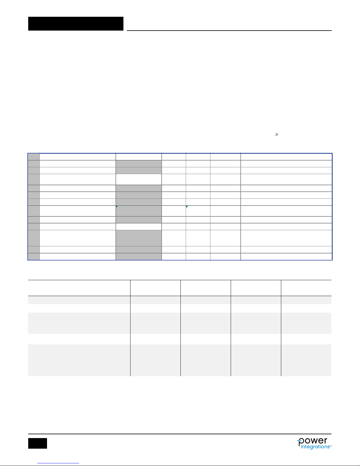
Basic Circuit Conguration
The circuit in Figure 1 shows the basic conguration of a yback
power supply designed using InnoSwitch3. Different output power
levels may require different values for some circuit components, but
the general circuit conguration remains similar. Advanced features
such as line overvoltage and undervoltage protection, primary or
secondary sensed output overvoltage protection and constant current
limit programming are implemented using very few passive components.
L
F
R
SN
R
LS1
BRD
F
R
L
C
R
T
N
O
t
C
1
F
2
B
C
SN
R
S
C
BIAS
InnoSwitch3
Primary FET
and Controller
power supplies is shown in Figure 1, which also serves as the
reference circuit for component identication used in the description
throughout this application note.
In addition to this application note, there is the InnoSwitch3 reference
design kit (RDK) containing an engineering prototype board as well
as device samples that provides an example of a working power
supply. Further details on downloading PI Expert, obtaining an RDK
and updates to this document can be found at www.power.com.
CY
R
FB(UPPER)
C
C
D
SN
D
BIAS
R
FWD
R
LS2
D V
S IS
BPP
R
BP
C
BPP
C
R
FB(LOWER)
FB
VOUT
Secondary
Control IC
FB
C
SR
R
SR
OUT
SR FET
C
BPS
GND
BPS
SR
FWD
PH
R
PH
V
OUT
R
IS
PI-8465-041818
RTN
Figure 1. Typical Adapter Power Supply Schematic using InnoSwitch3 with Line Undervoltage Lockout, Line Overvoltage Shutdown, Constant Output Current Limit
and Quasi-Resonant Synchronous MOSFET Rectier and Integrated Output Overvoltage Protection.
Scope
This application note is intended for engineers designing an isolated
AC-DC yback power supply or charger using the InnoSwitch3 family
of devices. It provides guidelines to enable an engineer to quickly
select key components and also complete a suitable transformer
design. To help simplify the task, this application note refers directly
to the PIXls designer spreadsheet that is part of the PI Expert™
design software suite available online (https://piexpertonline.power.
com/site/login). The basic conguration used in InnoSwitch3 yback
Quick Start
Readers familiar with power supply design and Power Integrations
design software may elect to skip the step by step design approach
described later, and can use the following information to quickly
design the transformer and select the components for a rst prototype.
For this approach, only the information described below needs to be
entered into the PIXls spreadsheet, other parameters will be
automatically selected based on a typical design. References to
spreadsheet line numbers are provided in square brackets [line
reference].
2
Rev. A 10/18
www.power.com
Page 3

Application NoteAN-72
• Enter AC input voltage range and line frequency, VAC_MIN [B3],
VAC_MAX [B4], LINEFREQ [B6]
• Enter input capacitance, CAP_INPUT [B7]
• 3 µF / W for universal (85-265 VAC) or single (100/115 VAC) line.
A more aggressive value of 2 µF / W can be used for many
charger designs that do not need to meet hold up time require-
ment
• Use 1 µF/W for 230 VAC or for single (185-265 VAC) line. If this
cell is left blank then the capacitance value for a VMIN of 70 V
(universal input) or 150 V (single 230 VAC) is calculated. Often
this will lead to an optimal input lter capacitance value
• Enter nominal output voltage, VOUT [B8]
• Enter desired cable drop compensation, PERCENT_CDC [B9]
• “0%” for no cable compensation
• “1% - 6%” for featured H-code trim
• Enter continuous output current, IOUT [B10]
• Enter efciency estimate, EFFICIENCY [B12]
• 0.83 for universal input voltage (85-265 VAC) or single 100/115
VAC (85-132 VAC) and 0.85 for a single 230 VAC (185-265 VAC)
design. Adjust the number accordingly after measuring the
efciency of the rst prototype-board at max load and VACMIN
• Select power supply enclosure, ENCLOSURE [B14]
• Select current limit mode, ILIMIT_MODE [B19]
• Two current limit congurations are available, STANDARD or
INCREASED
Output Power Table
230 VAC ± 15% 85-265 VAC
Product
INN3162C 10 W 12 W 10 W 10 W
INN3163C 12 W 15 W 12 W 12 W
INN3164C 20 W 25 W 15 W 20 W
INN3165C 25 W 30 W 22 W 25 W
INN3166C 35 W 40 W 27 W 36 W
INN3167C 45 W 50 W 40 W 45 W
INN3168C 55 W 65 W 50 W 55 W
Notes:
1. Minimum continuous power in a typical non-ventilated enclosed typical size
adapter measured at 40 °C ambient. Max output power is dependent on the
design. With condition that package temperature must be < 125 °C.
2. Minimum peak power capability.
3. Package: InSOP-24D.
3
Adapter
1
Open
Frame
2
Adapter
1
Open
Frame
• Select InnoSwitch3 from drop-down list or enter directly [B20]
• Select the device from Table 1 according to output power, input
voltage and application
• InnoSwitch3-CE for CV/CC yback application
• InnoSwitch3-EP for CV/CC yback application with 725 V
MOSFET
• Enter desired maximum switching frequency at full load, FSWITCH-
ING_MAX [B34]
• Enter desired reected output voltage, VOR [B35]
• Enter core type (if desired), CORE [B63] from drop down menu
• Suggested core size will be selected automatically if none is
entered [B63]
• For custom core, enter CORE CODE [B64], and core parameters
from [B65] to [B72]
• Enter secondary number of turns [B88]
If any warnings are generated, make changes to the design by
following instructions in spreadsheet column D.
• Build transformer as suggested in “Transformer Construction” tab
• Select key components
• Build prototype and iterate design as necessary, entering measured
values into spreadsheet where estimates were used (e.g. efciency,
V
). Note that the initial efciency estimate is very conservative.
MIN
Output Power Table
Product
2
3
INN3672C 12 W 10 W
INN3673C 15 W 12 W
INN3 674 C 25 W 20 W
INN3675C 30 W 25 W
INN3676C 40 W 36 W
INN3677C 45 W 40 W
Notes:
1. Minimum continuous power in a typical non-ventilated enclosed typical size
adapter measured at 40 °C ambient. Max output power is dependent on the
design. With condition that package temperature must be < 125 °C.
2. Minimum peak power capability.
3. Package: InSOP-24D.
230 VAC ± 15% 85-265 VA C
Peak or
Open Frame
1,2
Peak or
Open Frame
1,2
Table 1. Output Power Tables of InnoSwitch3-CE and EP.
www.power.com
3
Rev. A 10/18
Page 4
Application Note AN-72
APPLICATION VARIABLES
265
7 CAP_INPUT 40.0 uF Input capacitor
5.00
0%
Percentage (of output voltage) cable drop
10 IOUT 4.00 4.00 A Output current
AC-DC efficiency est imate at full load given that
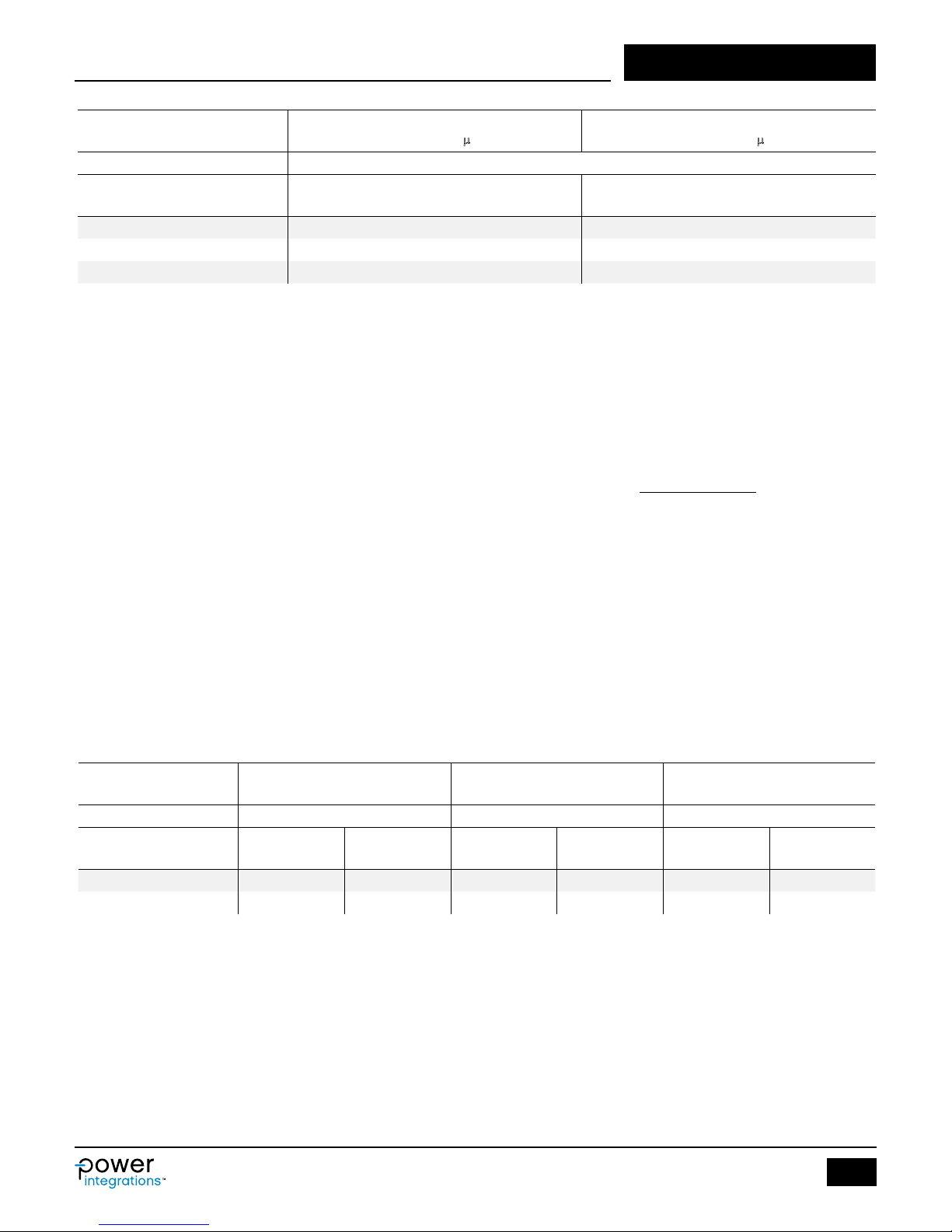
Step-by-Step Design Procedure
This design procedure uses the PI Expert design software (available
from Power Integrations), which automatically performs the key
calculations required for an InnoSwitch3 yback power supply design.
PI Expert allows designers to avoid the typical highly iterative design
process. Look-up tables and empirical design guidelines are provided
in this procedure where appropriate to simplify the design task.
Iterate the design to eliminate warnings. Any parameters outside the
recommended range of values can be corrected by following the
guidance given in the right hand column. Once all warnings have
been cleared, the output transformer design parameters can be used
to create a prototype transformer.
Step 1 ‒ Application Variables
Enter: VIN_MIN, VIN_MAX, LINEFREQ, CAP_INPUT, VOUT,
PERCENT_CDC, IOUT, EFFICIENCY, FACTOR _Z, and
ENCLOSURE
Minimum and Maximum Input Voltage, V_MIN, V_MAX (VAC)
Determine the input voltage range from Table 2 for a particular
regional requirement.
Line Frequency, LINEFREQ (Hz)
50 Hz for universal or single 100 VAC, 60 Hz for single 115 VAC input.
50 Hz for single 230 VAC input. These values represent typical line
frequencies rather than minimum. For most applications this gives
adequate overall design margin. For absolute worst-case or based on
the product specication reduce these numbers by 6% (47 Hz or 56 Hz).
Total Input Capacitance, CAP_INPUT (
µF)
Enter total input capacitance using Table 3 for guidance.
2
3 VIN_MIN 85 85 V Minimum AC input voltage
4 VIN_MAX
5 VIN_RANGE UNIVERSAL Range of AC input voltage
6 LINEFREQ 60 Hz AC Input voltage frequency
8 VOUT
9 PERCENT_CDC
265 V Maximum AC input voltage
5.00 V Output voltage at the board
0%
Design Title
compensation desired at full load
11 POUT 20.00 W Output power
12 EFFICIENCY 0.89 0.89
13 FACTOR_Z 0.50 Z-factor estimate
14 ENCLOSURE ADAPTER ADAPTER Power supply enclosure
Figure 2. Application Variable Section of InnoSwitch3-CE Design Spreadsheet with Gray Override Cells.
Region
Nominal Input
Voltage (VAC)
Minimum Input
Voltage (VAC)
the converter is switching at the valley of the
rectified minimum input AC voltage
Maximum Input
Voltage (VAC)
Japan 100 85 132 50 / 60
United States, Canada 120 90 132 60
Australia, China, European Union Countries,
India, Korea, Malaysia, Russia
230 185 265 50
Indonesia, Thailand, Vietnam 220 185 265 50
115, 120, 127 90 155 50 / 60
Rest of Europe, Asia, Africa, Americas
and rest of the world
220, 230 185 265 50 / 60
240 185 265 50
Visit: https://en.wikipedia.org/wiki/Mains_electricity_by_country
Table 2. Standard Worldwide Input Line Voltage Ranges and Line Frequencies.
Nominal Line
Frequency (Hz)
4
Rev. A 10/18
www.power.com
Page 5
Application NoteAN-72
TotalLosses
Secondary Losses
Total Input Capacitance per Watt of
Output Power (µF/W)
AC Input Voltage (VAC) Full Wave Rectication
Adapter with hold-up time requirement
100 / 115 3 2
230 1 1
85-265 3 2
Table 3. Suggested Total Input Capacitance for Different Input Voltage Ranges.
The capacitance is used to calculate the minimum and maximum DC
voltage across the bulk capacitor and should be selected to keep the
minimum DC input voltage, VMIN > 70 V.
Nominal Output Voltage, VOUT (V)
Enter the nominal output voltage of the main output at full load.
Usually the main output is the output from which feedback is derived.
Cable Compensation, PERCENT_CDC (%)
Select the appropriate cable compensation depending on the choice
of cable for the design. If this power supply is not supplied with a
cable, use the default 0%. (For InnoSwitch3-EP, this feature is not
available)
Power Supply Output Current, IOUT (A)
This is the maximum continuous load current of the power supply.
Output Power, POUT (W)
This is a calculated value and will be automatically adjusted based on
cable compensation selected.
Power Supply Efciency, EFFICIENCY (η)
Enter the estimated efciency of the complete power supply
measured from the input and output terminals under peak load
conditions and worst-case line (generally lowest input voltage). The
table below can be used as a reference. Once a prototype has been
constructed then the measured efciency should be entered and
further transformer iteration(s) can be performed if required.
Power Supply Loss Allocation Factor, FACTOR_ Z
This factor describes the apportioning of losses between the primary
and the secondary of the power supply. Z factor is used together
with the efciency to determine the actual power that must be
delivered by the power stage. For example losses in the input stage
(EMI lter, rectication etc) are not processed by the power stage
(transferred through the transformer) and therefore although they
reduce efciency the transformer design is not effected.
For designs that do not have a peak power requirement, a value of
0.5 is recommended. For designs with a peak power requirement
enter 0.65. The higher number indicates larger secondary side
losses.
Enclosure
Power device selection will also be dependent on the application
environment. For an open frame application where the operating
ambient temperature is lower than in an enclosed adapter, the PIXls
will suggest a smaller device for the same output power.
Efciency is also a function of output power, low power designs are
most likely around 84% to 85% efcient, whereas with a synchronous
rectier (SR) the efciency would reach 90% typically.
Total Input Capacitance per Watt of
Output Power (µF/W)
Open Frame or Charger/Adapter without
hold-up time requirement
Z =
Nominal Output
Voltage (VOUT)
5 0.84 0.87 0.84 0.88 0.87 0.89
12 0.86 0.90 0.86 0.90 0.88 0.90
Table 4. Efciency Estimate Without Output Cable .
www.power.com
Typical Low-Line Range Typical Universal Range Typical High-Line Range
85 VAC - 132 VAC 85 VAC - 265 VAC 185 VAC - 265 VAC
Schottky Diode
Rectier
Synchronous
Rectier
Schottky Diode
Rectier
Synchronous
Rectier
Schottky Diode
Rectier
Synchronous
Rectier
5
Rev. A 10/18
Page 6
Application Note AN-72
18 PRIMARY CONTROLLER SELECTION
19 ILIMIT_MODE STANDARD STANDARD Device current limit mode
Auto
21 DEVICE_CODE INN3165C Actual device code
Power capability of the device based on thermal
23 RDSON_100DEG 3.47 Ω
Primary MOSFET on time drain resistance at 100
degC
24 ILIMIT_MIN 0.88 A Minimum current limit of the primary MOSFET
26 ILIMIT_MAX 1.02 A Maximum c urrent limit of the primary MOSFET
27 VDRAIN_BREAKDOWN 650 V Device breakdown voltage
Peak drain voltage on the primary MOSFET
Step 2 – Primary Controller Selection
Enter: Device Current Limit mode, ILIMIT and Generic Device
Code, DEVICE_GENERIC
20 DEVICE_GENERIC
22 POUT_MAX 22 W
25 ILIMIT_TYP 0.95 A Typical current limit of the primary MOSFET
28 VDRAIN_ON_MOSFET 0.87 V Primary MOSFET on time drain voltage
29 VDRAIN_OFF_MOSFET 508.4 V
Figure 3. Primary Controller Selection of InnoSwitch3-CE Design Spreadsheet with Current Limit Mode Selection.
Generic Device Code, DEVICE_GENERIC
The default option is automatically selected based on input voltage
range, maximum output power and application (i.e. adapter or open
frame).
For manual selection of device size, refer to the InnoSwitch3 power
table in the data sheet and select a device based on the peak output
power. Then compare the continuous power to adapter column
numbers in the power table, (if the power supply is of fully enclosed
type), or compare to the open-frame column (if the power supply is
an open-frame design). If the continuous power exceeds the value
given in the power table (Table 1), then the next larger device should
be selected. Similarly, if the continuous power is close to the
maximum adapter power given in the power table, it may be
necessary to switch to a larger device based on the measured
thermal performance of the prototype.
Device Current Limit Mode, ILIMIT_MODE
For designs where thermals are not as challenging (such as open
frame applications) and lowest cost is a critical requirement, ILIMIT
MODE allows the choice of an INCREASED current limit mode, this
INN31X5 Generic device code
performance
during turn-off
will set the peak current of the device equivalent to the next bigger
device’s current limit and allow higher output power. By default,
ILIMIT is set to STANDARD.
On-Time Drain Voltage, VDRAIN_ON_MOSFET (V)
This parameter is calculated based on RDSON_100DEG and primary
RMS current.
Drain Peak Voltage, VDRAIN_OFF_MOSFET (V)
This parameter is the assumed Drain voltage seen by the device
during off-time. The calculation assumes 10% minimum margin from
the breakdown voltage rating of the internal MOSFET and gives a
warning if this is exceeded.
VDRAIN < (VIN_MAX * 1.414) + VOR + VLK
VLK
is the voltage induced by the leakage inductance of the
PRI
transformer when MOSFET turns off.
PRI
– (BV
× 10 %).
DSS
Other electrical parameters are displayed based from the data sheet,
RDSON_100DEG, ILIMIT_MIN, ILIMIT_TYP, ILIMIT_MAX,
VDRAIN_BREAKDOWN.
6
Rev. A 10/18
www.power.com
Page 7
WORST CASE ELECTRICAL
34 FSWITCHING_MAX 80000 80000 Hz
Maximum s witching frequency at full load and
valley of the rectified minimum AC input voltage
Seconday voltage reflected to the primary when
36 VMIN 85.95 V
Valley of the rectified minimum AC input voltage
at full power
Measure of continuous/discontinuous mode of
39 DUTYCYCLE 0.433 Primary MOSFET duty cy cle
42 LPRIMARY_MIN 805.6 uH Minimum primary inductance
3.0
45 LPRIMARY_MAX 855.4 uH Maximum primary inductance
48 IPEAK_PRIMARY 0.95 A Primary MOSFET peak currrent
51 IRIPPLE_PRIMARY 0.76 A Primary MOSFET ripple current
54 SECONDARY CURRENT
Step 3 – Worst-Case Electrical Parameters
Enter: FSWITCHING_MAX, VOR and LPRIMARY_TOL, or VMIN
33
PARAMETERS
Application NoteAN-72
35 VOR 65.0 V
37 KP 0.66
38 MODE_OPERATION CCM Mode of operation
40 TIME_ON 7.46 us Primary MOSFET on-time
41 TIME_OFF 7.09 us Primary MOSFET off-time
43 LPRIMARY_TYP 830.5 uH Typical primary inductance
44 LPRIMARY_TOL
46
47 PRIMARY CURRENT
49 IPEDESTAL_PRIMARY 0.30 A Primary MOSFET current pedestal
50 IAVG_PRIMARY 0.25 A Primary MOSFET average current
52 IRMS_PRIMARY 0.41 A Primary MOSFET RMS current
53
55 IPEAK_SECONDARY 12.24 A Secondary winding peak current
56 IPEDESTAL_SECONDARY 3.79 A Secondary winding current pedestal
57 IRMS_SECONDARY 6.44 A Secondary winding RMS current
Figure 4. Worst-Case Electrical Parameters Section of InnoSwitch3-CE Design Spreadsheet with Gray Override Cells.
3.0 % Primary inductance tolerance
the primary MOSFET turns off
operation
Switching Frequency, FSWITCHING_MAX (Hz)
This parameter is the switching frequency at full load at minimum
rectied AC input voltage. The maximum switching frequency of
InnoSwitch3 in normal operation is 100 kHz, and the typical overload
detection frequency of is 110 kHz. In normal operating condition, the
switching frequency at full load should not be close to the overload
detection frequency.
The programmable switching frequency range is 25 to 95 kHz, but it
should be continued that the average frequency accounting for
primary inductance and peak current tolerances does not result in
average frequency higher than 110 kHz as this will trigger autorestart due to overload. Pushing frequency higher to reduce
InnoSwitch3 Family Maximum Switching Frequency
INN3xx2C and
INN3xx3C
INN3xx4C and
INN3xx5C
INN3xx6C 75 kHz
INN3xx7C 70 kHz
INN3xx8C 65 kHz
Table 5. Suggested Maximum Switching Frequency.
transformer size is advisable, but Table 5 provides the suggested
frequency based on the size of the internal high-voltage MOSFET, and
represents the best compromise to balance overall device losses (i.e.
conduction and switching losses).
Reected Output Voltage, VOR (V)
This parameter is the secondary winding voltage during the diode /
Synchronous Rectier MOSFET (SR FET) conduction-time reected
back to the primary through the turns ratio of the transformer. Table
6 provides suggested values of VOR. VOR can be adjusted to achieve
SR FET while simultaneously achieving sufciently low Drain-Source
voltage of the primary side MOSFET. VOR can be adjusted as
necessary to ensure that no warnings in the spreadsheet are
triggered. For design optimization purposes, the following factors
should be considered,
• Higher VOR allows increased power delivery at VMIN, which
minimizes the value of the input capacitor and maximizes power
delivery from a given.
a design that does not violate design rules for the transformer and
www.power.com
85 - 90 kHz
80 kHz
7
Rev. A 10/18
Page 8
Application Note AN-72
• Higher VOR reduces the voltage stress on the output diodes and SR
FETs, which in some cases may allow a lower voltage rating for
higher efciency.
• Higher VOR increases leakage inductance which reduces power
supply efciency.
• Higher VOR increases peak and RMS current on the secondary-side
which may increase secondary side copper, diode and SR FET losses
thereby reducing efciency.
It should be noted that there are exceptions to this guidance
especially for very high output currents where the VOR should be
reduced to obtain highest efciency. Higher output voltages
(above 15 V) should employ a higher VOR to maintain acceptable
peak inverse voltage (PIV) across the output SR FET.
Optimal selection of the VOR value depends on the specic
application and is based on a compromise between the factors
mentioned above.
Output
Voltage
Suggested VOR
Value
Suggested
Range
5 V 55 V 45 V - 60 V
9 V 85 V 80 V - 90 V
12 V - 20 V 110 V 100 V - 120 V
Table 6. Suggested Values for VOR.
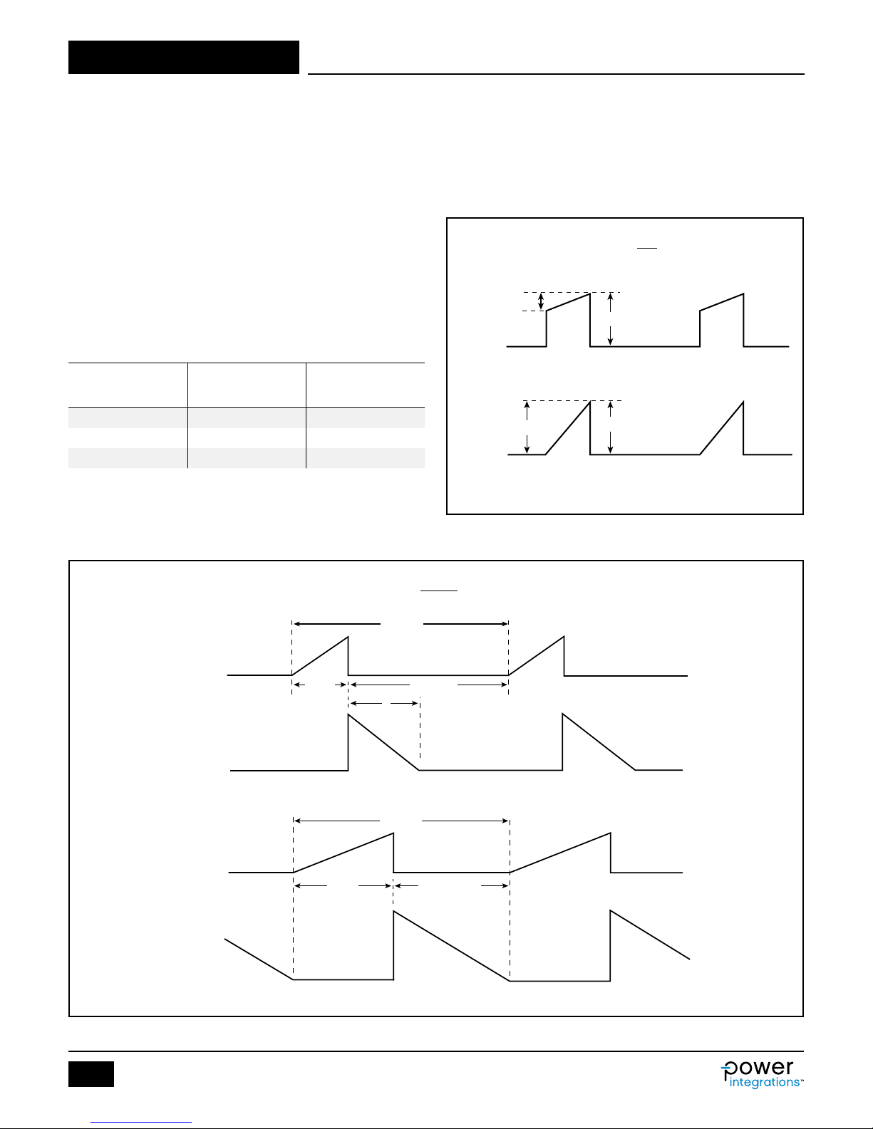
Mode of Operation, KP
KP is a measure of how discontinuous or continuous the mode of
switching is. KP > 1 is said to be in discontinuous operation (DCM),
while KP < 1 denotes continuous operation (CCM).
Ripple to Peak Current Ratio, K
Below 1 (indicating continuous conduction mode), KP is the ratio of
P
ripple to peak primary current (Figure 5).
I
KP ≡ KRP =
I
R
Primary
(a) Continuous, K
Primary
R
(b) Borderline Continuous/Discontinuous, K
P
< 1
R
I
P
I
P
I
PI
= 1
P
PI-2587-103114
Primary
Secondary
Primary
Secondary
D × T
(a) Discontinuous, K
D × T
KP ≡ KDP =
> 1
P
T = 1/f
t
T = 1/f
Figure 5. Continuous Mode Current Waveform, K
(1-D) × T
t
S
(1-D) × T
S
(1-D) × T = t
P
≤1.
(b) Borderline Discontinuous/Continuous, K
Figure 6. Discontinuous Mode Current Waveform, KP≥1.
8
Rev. A 10/18
= 1
P
PI-2578-103114
www.power.com
Page 9

Application NoteAN-72
I
I
P
DT
VV D
VD
#
-
^
^
h
h
KK
/ =
PRP
Above a value of 1, indicating discontinuous conduction mode, KP is
the ratio of primary MOSFET off time to the secondary SR_FET
conduction time.
/ =
KK
PDP
#
OR MAX
=
MIN DS MAX
The value of KP should be in the range of 0.5 < KP < 6. Guidance is
given in the comments cell if the value of KP is outside this range.
Experience has shown that a KP value between 0.8 and 1 will result in
higher efciency by ensuring DCM or critical mode operation (CRM)
which is desirable for most charger designs.
The spreadsheet will calculate the values of peak primary current,
primary RMS current, primary ripple current, primary average current,
and the maximum duty cycle for the design based on the selection of
the these parameters.
Typical Primary Inductance, LPRIMARY_TYP (µH)
This is the typical transformer primary inductance target.
R
-
1
#
t
^
1
h
-
Primary Inductance Tolerance, LPRIMARY_TOL (%)
This parameter is the assumed primary inductance tolerance. A value
of 7% is used by default, however if specic information is provided
from the transformer vendor, then this may be entered in the grey
override cell. A value of 7% helps to reduce unit-to-unit variation and
is easy to meet for most magnetics vendors. A value of 3% will help
improve production tolerance further but will be more challenging to
vendors.
The other important electrical parameters are automatically calculated
by the spreadsheet. These can used to appropriatley select the other
components in the circuit, such as input fuse (FR) and EMI lter (LF),
bridge rectiers (BRD), output rectiers (SR
as described in Figure 1.
PRIMARY CURRENT
IPEAK_PRIMARY − Peak primary current
IPEDESTAL_PRIMARY − Primary MOSFET current pedestal in CCM mode
IAVG_PRIMARY − Primary MOSFET average current
IRIPPLE_PRIMARY − Primary MOSFET ripple current
IRMS_PRIMARY − Primary MOSFET RMS current
SECONDARY CURRENT
IPEAK_SECONDARY − Peak secondary current
IPEDESTAL_SECONDARY − Secondary winding current pedestal
IRMS_SECONDARY − Secondary winding RMS current
Minimum Rectied Input Voltage, VMIN
Valley of the rectied minimum AC input voltage at full power is
calculated based on input capacitance (CAP_INPUT).
) and capacitors (C
FET
OUT
),
www.power.com
9
Rev. A 10/18
Page 10
Application Note AN-72
TRANSFORMER CONSTRUCTION
PARAMETERS
CORE SELECTION
63 CORE RM6 Info RM6
The transformer windings may not fit: pic k a
Parameters tab for fit calculations
66 LE 29.20 mm Core magnetic path length
Safety margin width (Half the primary to
74 PRIMARY WINDING
77 BMAX 2844 Gauss Maximum flux density
80 LG 0.310 mm Core gap length
4
Primary winding wire outer diameter with
Primary winding wire outer diameter without
85 CMA_PRIMARY 248 Cmil/A Primary winding wire CMA
SECONDARY WINDING
88 NSECONDARY 6 6 Secondary turns
Secondary winding wire outer diameter with
Secondary winding wire outer diameter without
BIAS WINDING
Step 4 – Transformer Construction Parameters
Enter: CORE, AE, LE, AL, VE, BOBBIN, AW, BW, MARGIN
Choose Core and Bobbin based on maximum output power.
61
62
bigger core or bobbin and refer to the Transformer
64 CORE CODE PC95RM06Z Core code
65 AE 37.00 mm^2 Core cross sectional area
67 AL 2150 nH/turns^2 Ungapped core effective inductance
68 VE 1090.0 mm^3 Core volume
69 BOBBIN B-RM06-V Bobbin
70 AW 15.52 mm^2 Window area of the bobbin
71 BW 6.20 mm Bobbin width
72 MARGIN 0.0 mm
73
75 NPRIMARY 77 Primary turns
76 BPEAK 3125 Gauss Peak flux density
78 BAC 933 Gauss AC flux density
79 ALG 140 nH/turns^2 Typical gapped core effective inductance
81 LAYERS_PRIMARY
82 AWG_PRIMARY 30 AWG Primary winding wire AWG
83 OD_PRIMARY_INSULATED 0.303 mm
84 OD_PRIMARY_BARE 0.255 mm
86
87
89 AWG_SECONDARY 19 AWG Secondary winding wire AWG
90 OD_SECONDARY_INSULATED 1.217 mm
91 OD_SECONDARY_BARE 0.912 mm
92 CMA_SECONDARY 216 Cmil/A Secondary winding wire CMA
93
94
95 NBIAS 15 Bias turns
4 Number of primary layers
secondary creepage distance)
insulation
insulation
insulation
insulation
Figure 7. Transformer Core and Construction Variables Section of InnoSwitch3 PIXLs Spreadsheet.
Core Type, CORE
By default, if the core type cell is left empty, the spreadsheet will
select the smallest commonly available core suitable for the
continuous (average) output power specied. Different core types
and sizes from the drop-down list are available to choose from if a
user-preferred core is not available, the grey override cells (AE, LE,
AL, VE, AW & BW) can be used to enter the core and bobbin
parameters directly from the manufacturer’s data sheet.
10
Rev. A 10/18
www.power.com
Page 11
Application NoteAN-72
Core and Bobbin Table
Core Bobbin
Output
Power at
Core Code
75 kHz
0 W ‒ 10 W EE10
PC47EE10-Z
0 W ‒ 10 W EE13 PC47EE13-Z 17.1 30.2 1130 517 B-EE13-H 18.43 7.60
0 W ‒ 10 W EE16 PC47EE16-Z 19.2 35.0 1140 795 B-EE16-H 14.76 8.50
0 W ‒ 10 W EE19 PC47EE19-Z 23.0 39.4 1250 954 B-EE19-H 29.04 8.80
10 W ‒ 20 W EE22 PC47EE22-Z 41.0 39.4 1610 1620 B-EE22-H 19.44 8.45
10 W ‒ 20 W EE25 PC47EE25-Z 41.0 47.0 2140 1962 B-EE25-H 62.40 11.60
20 W ‒ 50 W EE30 PC47EE30-Z 111.0 58.0 4690 6290 B-EE30-H 13.20
0 W ‒ 10 W RM5 PC95RM05Z 24.8 23.2 2000 574 B-RM05-V 4.90
10 W ‒ 20 W RM6 PC95RM06Z 37.0 29.2 2150 1090 B-RM06-V 6.20
20 W ‒ 30 W RM8 PC95RM08Z 64.0 38.0 5290 2430 B-RM08-V 30.00 8.80
30 W ‒ 50 W RM10 PC95RM10Z 96.6 44.6 4050 4310 B-RM10-V 10.00
Table 7. Commonly Available Cores and Power Levels at Which These Cores Can be used for Typical Designs.
AE LE AL VE
2
) (mm) (nH/T2) (mm3) (mm2) (mm)
(mm
Code
AW BW
12.1 26.1 850 300 B-EE10-H 12.21 6.60
Safety Margin, MARGIN (mm)
For designs that require safety isolation between primary and
secondary, but are not using triple insulated wire the width of the
safety margin to be used on each side of the bobbin should be
entered here. Typically for universal (85 – 265 VAC) input designs a
total margin of 6.2 mm is required, and a value of 3.1 mm should be
entered into the spreadsheet. For vertical bobbins the margin may
not be symmetrical; however if a total margin of 6.2 mm is required
then 3.1 mm would still be entered even if the physical margin was
only present on one side of the bobbin. For designs using triple
insulated wire it may still be necessary to enter a small margin in
order to meet the required safety creepage distances. Typically
several bobbins exist for each core size and each will have different
mechanical spacing. Refer to the bobbin data sheet or seek guidance
to determine what specic margin is required.
Margin reduces the available area for the windings, marginated
construction may not be suitable for small core sizes. If after
entering the margin more than 3 primary layers are required, it is
suggested that either a larger core be selected or that the design is
switched to a zero margin approach using triple insulated wire.
Primary Turns, NPRIMARY
This is the number of turns for the main winding of the transformer
calculated based on VOR and Secondary Turns.
Peak Flux Density, BPEAK (Gauss)
A maximum value of 3800 gauss is recommended to limit the peak
ux density at max current limit and 132 kHz operation. Under an
output-shorted condition the output voltage is low and little reset of
the transformer occurs during the MOSFET off-time. This allows the
transformer ux density to “staircase” beyond the normal operating
level. A value of 3800 gauss at the max current limit of the selected
device together with the built in protection features of InnoSwitch3
provides sufcient margin to prevent core saturation under output
short-circuit conditions.
Maximum Flux Density, BMAX (Gauss)
The low frequency operation resulting from a light load condition can
generate audible frequency components within the transformer,
especially if a long core is used. To limit audible noise generation,
the transformer should be designed such that the maximum core ux
density is below 3000 gauss (300 mT). Following this guideline and
using the standard transformer production technique of dip varnishing
practically eliminates audible noise. A careful evaluation of the
audible noise performance should be made using production
transformer samples before approving the design.
AC Flux Density, BAC (Gauss)
The BAC value can be used for calculating core loss.
Gapped Core Effective Inductance, ALG: (nH/N
2
)
Used to specify the CORE GAP [LG].
Primary Layers, LAYERS_PRIMARY
By default, if the override cell is empty, a value of 3 is assumed.
Primary layers should be in the range of 1 ≤ L ≤ 3, and in general it
should meet the current capacity guideline of 200 – 500 circular mils/
ampere for designs without forced air cooling. Primary winding wire
gauge AWG_PRIMARY is calculated in cell [E82]. Values above 3
layers are possible but the increased leakage inductance and physical
t of the windings should be considered. A split primary construction
may be helpful for designs where leakage inductance clamp
dissipation is too high. In this approach half of the primary winding is
placed on either side of the secondary (and bias) windings in a
sandwich arrangement.
Primary Winding Wire Guage, AWG_PRIMARY (AWG)
By default, if the override cell is empty, double insulated wire is
assumed and a standard wire diameter is chosen. The grey override
cells can be used to enter the wire gauge directly by the user, or if
the wire used is different from the standard double insulated type.
www.power.com
11
Rev. A 10/18
Page 12

Application Note AN-72
99 PRIMARY COMPONENTS SELECTION
100 Line unde rvoltage
74.0
102 RLS 3.74 MΩ
Connect two 1.87 MOhm resistors to t he V-pin for
the required UV/OV threshold
105
Line overvoltage
107 OVERVOLTAGE_LINE 312.5 V Actual AC RMS line over-voltage threshold
108
Bias diode
110 VBIAS 12.0 V Rectified bias voltage
111 VF_BIAS 0.70 V Bias winding diode forward drop
Bias diode reverse voltage (not accounting
113 CBIAS 22 uF Bias winding rectification capacitor
Secondary Turns, NSECONDARY
By default, if the grey override cell is left blank, the minimum number
of secondary turns is calculated such that the peak operating ux
density B
gauss (380 mT). In general, it is not necessary to enter a number in
is kept below the recommended maximum of 3800
PEAK
the override cell except in designs where a lower operating ux
density is desired.
Bias Turns, NBIAS
Determined based on VBIAS set voltage or secondary turns.
The other transformer parameters that are automatically calculated
by the spreadsheet include:
OD_PRIMARY_INSULATED (mm), Primary winding wire outer
diameter with insulation
OD_PRIMARY_BARE (mm), Outer diameter without insulation
CMA_PRIMARY (Cmil/A), Winding CMA
OD_SECONDARY_INSULATED (mm), Secondary winding wire
outer diameter with insulation
OD_ SECONDARY _BARE (mm), Outer diameter without insulation
CMA_ SECONDARY (Cmil/A), Winding CMA
Step 5 – Primary Components Selection
Enter: BROWN-IN VOLTAGE, VBIAS, VF_BIAS
101 BROWN-IN REQURED
Brown-Out Actual
During brown-out, the power supply will inhibit switching when the
brown-out threshold current falls below the IUV- threshold.
Line Overvoltage, OVERVOLTAGE_LINE
This is the input AC voltage at which the power supply will
instantaneously stop switching once the overvoltage threshold (I
is exceeded, switching will be re-enabled when switching the line
overvoltage hysteresis (I
approximately equal to I
) level is reached. Line OV voltage is
OV(H)
× (RLS1 + RLS2) / 1.414.
OV+
OV+
)
Rectied Bias Voltage, VBIAS
A default value of 12 V is assumed. The voltage may be set to
different values (for example for applications when the bias winding
output is also used as a non-isolated primary-side auxiliary output).
Higher voltages t ypically increase no-load input power. Values below
10 V are not recommended since at light load there may be insufcient
voltage to supply current to the PRIMARY BYPASS pin which will
increase no-load input power. A 22 µF, 50 V low ESR electrolytic
capacitor is recommended for the bias winding rectication lter
capacitor, CBIAS. A low ESR electrolytic capacitor improves no-load
input power.
BPP Pin Capacitor, CBPP
The capacitance value is determined by the ILIMIT_MODE required.
0.47 µF for standard or 4.7 µF for increased current limit. Although
74.0 V Required AC RMS line voltage brown-in threshold
103 BROWN-IN ACTUAL 75.0 V Ac tual AC RMS brown-in threshold
104 BROWN-OUT ACTUAL 67.8 V Ac tual AC RMS brown-out threshold
106
109
112 VREVERSE_BIASDIODE 84.73 V
114 CBPP 0.47 uF BPP pin c apacitor
Figure 8. Primary Components Section of InnoSwitch3 PIXls Spreadsheet.
Required Line Undervoltage Brown-in, BROWN-IN REQUIRED
This is the input AC voltage at which the power supply will turn on
(once the brown-in threshold (IUV+) is exceeded). The typical value
is 20% below minimum AC input voltage (VIN_MIN). The brown-in
voltage can be changed to a specic voltage required on cell [C101].
Line Undervoltage / Overvoltage Sense Resistor, RLS
PIXls will calculate the resistance value based on the brown-in
electrolytic capacitors can be used, often surface mount multi-layer
ceramic capacitors are preferred for use on double sided boards as
they enable placement of capacitors close to the IC. A ceramic X7R
(or better) type capacitor rated to at least 25 V is recommended.
Bias Diode Forward Drop, VF_BIAS
A default value of 0.7 V is used though this can be changed to match
the type of diode used for rectifying the bias winding.
parasitic voltage ring)
voltage. Shown as RLS1 + RLS2 on Figure 13, they are typically
connected after the bridge rectier. Typical total value for RLS1 +
RLS2 is 3.8 MΩ. RLS is approximately equal to V
BROWN -IN
× 1.414 / I
UV+
.
12
Rev. A 10/18
www.power.com
Page 13

Application NoteAN-72
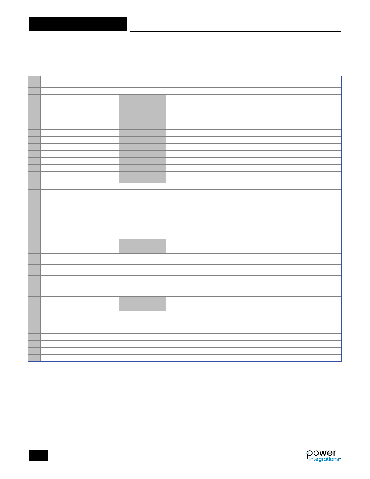
SECONDARY COMPONENTS
119 RFB_UPPER 100.00 kΩ
Upper feedback resistor (connected to the first
output voltage)
125 MULTIPLE OUTPUT PARAMETERS
OUTPUT 1
128 IOUT1 4.00 A Output 1 c urrent
Root mean squared value of the secondary
131 IRIPPLE_CAP_OUTPUT1 4.41 A
Current ripple on the secondary waveform for
output 1
133 OD_SECONDARY1_INSULATED 1.217 mm
Secondary winding wire outer diameter with
insulation for output 1
Secondary winding wire outer diameter without
135 CM_SECONDARY1 1191 Cmils
Bare conductor effective area in circular mils for
output 1
SRFET reverse voltage (not accounting parasitic
138 SRFET1 Auto AON6266 SRFET selection for output 1
SRFET on-time drain resistance at 25degC and
Step 6 – Secondary Components
Enter: RFB_UPPER
118
120 RFB_LOWER 34.00 kΩ Lower feedback resistor
121 CFB_LOWER 330 pF Lower feedback resistor decoupling capacitor
Figure 9. Secondary Components Section of InnoSwitch3 PIXLs Spreadsheet.
126
127 VOUT1 5.00 V Output 1 voltage
129 POUT1 20.00 W Output 1 power
130 IRMS_SECONDARY1 5.95 A
132 AWG_SECONDARY1 19 AW G W ire size for output 1
134 OD_SECONDARY1_BARE 0.912 mm
136 NSECONDARY1 6 Number of turns for output 1
137 VREVERSE_RECTIFIER1 34.09 V
139 VF_SRFET1 0.076 V SRFET on-time drain voltage for output 1
140 VBREAKDOWN_SRFET1 60 V SRFET breakdown voltage for output 1
141 RDSON_SRFET1 19.0 mΩ
Figure 10. Secondary Components Section of InnoSwitch3 PIXls Spreadsheet.
Upper Feedback Resistor, RFB_UPPER
The RFB_UPPER resistor value is calculated based on VOUT and the
nominal internal reference voltage of the IC (1.265 V).
Upper Feedback Resistor, RFB_LOWER
The RFB_LOWER resistor is calculated based on VOUT and the 1.265 V
internal reference voltage. The value will change if the specied
value is used for the RFB_UPPER resistor.
Lower Feedback Resistor Decoupling Capacitor, CFB_LOWER
A 330 pF surface mount ceramic X7R type capacitor (or better) is
recommended as this can be placed close to the pins of the FEEDBACK
and GROUND pins of the IC.
Step 7 – Multiple Output Parameters
This section allows the user to design up to three secondary outputs
(excluding bias supply) and choose a suitable MOSFET size for
synchronous rectication. The spreadsheet will provide a warning
should the total power of the multiple outputs exceed the power
Each output provides a selection of synchronous rectier MOSFETs
(SRFET) in the drop down menu, (see Table 10). Based on the SR
FET chosen the on-state forward voltage, VF_SRFET (V), breakdown
voltage, VBREAKDOWN_SRFET (V), and on-time drain resistance,
RDSON_SRFET (m
The spreadsheet also calculates the critical electrical parameters for
each secondary output:
RMS Current of the Secondary Output, RMS_SECONDARY (A)
– Used to size the secondary winding wire.
Current Ripple on Secondary, IRIPPLE_CAP_OUTPUT (A)
– Used to size the output lter capacitor.
–Number of Turns for Output, NSECONDARY
– Calculated turns for each output.
Additional information for the magnetic wire are also given, AWG _
SECONDARY (AWG), OD_SECONDARY_INSULATED (mm) and
OD_SECONDARY_BARE (mm).
current for output 1
insulation for output 1
voltage ring) for output 1
VGS=4.4V for output 1
Ω) will be displayed in the spreadsheet.
described in the POUT cell.
For single output design, cells VOUT1, IOUT1 and POUT1 will be
the main output parameters entered in section 1.
www.power.com
13
Rev. A 10/18
Page 14

Application Note AN-72
OUTPUT 2
145 IOUT2 0.00 A Output 2 c urrent
Root mean squared value of the secondary
148 IRIPPLE_CAP_OUTPUT2 0.00 A
Current ripple on the secondary waveform for
output 2
150 OD_SECONDARY2_INSULATED 0.000 mm
Secondary winding wire outer diameter with
insulation for output 2
Secondary winding wire outer diameter without
152 CM_SECONDARY2 0 Cmils
Bare conductor effective area in circular mils for
output 2
153 NSECONDARY2 0 Number of turns for output 2
SRFET reverse voltage (not accounting parasitic
155 SRFET2 Auto NA SRFET selection for output 2
158 RDSON_SRFET2 NA mΩ
SRFET on-time drain resistance at 25degC and
VGS=4.4V for output 2
161 VOUT3 0.00 V Output 3 voltage
Root mean squared value of the secondary
Current ripple on the secondary waveform for
166 AWG_SECONDARY3 0 AWG W ire size for output 3
Secondary winding wire outer diameter with
168 OD_SECONDARY3_BARE 0.000 mm
Secondary winding wire outer diameter without
insulation for output 3
Bare conductor effective area in circular mils for
SRFET reverse voltage (not accounting parasitic
Auto
173 VF_SRFET3 NA V SRFET on-time drain voltage for output 3
SRFET on-time drain resistance at 25degC and
176
If negative output exis ts, enter the output number;
143
144 VOUT2 0.00 V Output 2 voltage
146 POUT2 0.00 W Output 2 power
147 IRMS_SECONDARY2 0.00 A
149 AWG_SECONDARY2 0 AWG W ire size for output 2
151 OD_SECONDARY2_BARE 0.000 mm
154 VREVERSE_RECTIFIER2 0.00 V
156 VF_SRFET2 NA V SRFET on-time drain voltage for output 2
157 VBREAKDOWN_SRFET2 NA V SRFET breakdown voltage for output 2
159
160 OUTPUT 3
162 IOUT3 0.00 A Output 3 c urrent
163 POUT3 0.00 W Output 3 power
164 IRMS_SECONDARY3 0.00 A
165 IRIPPLE_CAP_OUTPUT3 0.00 A
current for output 2
insulation for output 2
voltage ring) for output 2
current for output 3
output 3
167 OD_SECONDARY3_INSULATED 0.000 mm
169 CM_SECONDARY3 0 Cmils
170 NSECONDARY3 0 Number of turns for output 3
171 VREVERSE_RECTIFIER3 0.00 V
172 SRFET3
174 VBREAKDOWN_SRFET3 NA V SRFET breakdown voltage for output 3
175 RDSON_SRFET3 NA mΩ
177 PO_TOTAL 20.00 W Total power of all outputs
178 NEGATIVE OUTPUT N/A N/A
NA SRFET selection for output 3
insulation for output 3
output 3
voltage ring) for output 3
VGS=4.4V for output 3
e.g. If VO2 is negative output, select 2
Figure 11. Continuation of Multiple Output Parameters Section of InnoSwitch3 PIXls Spreadsheet.
14
Rev. A 10/18
www.power.com
Page 15

Step 8 ‒ Tolerance Analysis
182 TOLERANCE ANALYSIS
183 CORNER_VAC 85 V Input AC RMS voltage corner to be evaluated
TYP
185 CORNER_LPRIMARY TYP 830.5 uH Primary inductance c orner to be evaluated
Measure of continuous/discontinuous mode of
188 FSWITCHING 67267 Hz
Switching frequency at full load and valley of the
rectified minimum AC input voltage
190 TIME_ON 6.44 us Primary MOSFET on-time
191 TIME_OFF 8.43 us Primary MOSFET off-time
193 IPEDESTAL_PRIMARY 0.25 A Primary MOSFET current pedestal
194 IAVERAGE_PRIMARY 0.25 A Primary MOSFET average current
196 IRMS_PRIMARY 0.40 A Primary MOSFET RMS c urrent
197 CMA_PRIMARY 252 Cmil/A Primary winding wire CMA
This is a useful part of the InnoSwitch3 PIXls designer spreadsheet
that provides the user with switching parameters such as switching
frequency (FSWITCHING) for corner limits of device current limit
CORNER_ILIMIT and primary inductance of transformer
CORNER_LPRIMARY.
Application NoteAN-72
184 CORNER_ILIMIT
186 MODE_OPERATION CCM Mode of operation
187 KP 0.728
189 DUTYCYCLE 0.433 Steady state duty c ycle
192 IPEAK_PRIMARY 0.91 A Primary MOSFET peak currrent
195 IRIPPLE_PRIMARY 0.66 A Primary MOSFET ripple current
198 BPEAK 2835 Gauss Peak fux density
199 BMAX 2641 Gauss Maximum flux density
Figure 12. Tolerance Analysis Section of InnoSwitch3 PIXls Spreadsheet.
0.95 A Current limit c orner to be evaluated
operation
www.power.com
15
Rev. A 10/18
Page 16

Application Note AN-72
Step 9 – Critical External Components Selection
The schematic in Figure 13 shows the key external components
required for a practical single output InnoSwitch3 design. Component
selection criteria is as follows:
L
F
R
SN
R
LS1
BRD
F
R
L
C
R
T
N
O
t
C
1
F
2
B
C
SN
R
S
C
BIAS
InnoSwitch3
Primary FET
and Controller
Secondary Bypass Pin Capacitor (C
This capacitor works as a supply decoupling capacitor for the
BPS
)
secondary-side controller. A surface-mount, 2.2 µF, 25 V, multi-layer
ceramic capacitor is recommended for satisfactory operation of the
IC. The SECONDARY BYPASS Pin voltage needs to reach 4.4 V before
the output voltage reaches its target voltage. A signicantly higher
CY
R
FB(UPPER)
C
C
SR
D
SN
D
BIAS
R
FWD
R
LS2
D V
S IS
BPP
R
BP
C
BPP
R
FWD
SR
SR FET
SR
C
GND
OUT
R
C
BPS
BPS
Secondary
Control IC
C
FB
FB(LOWER)
FB
VOUT
PH
R
PH
V
OUT
R
IS
Figure 13. Typical InnoSwitch3 Flyback Power Supply.
Primary Bypass Pin Capacitor (C
This capacitor works as a supply decoupling capacitor for the internal
BPP
)
primary-side controller and determines current limit for the internal
MOSFET. For a 4.7 µF or 0.47 µF capacitor select either increased or
standard current limit respectively. All though electrolytic capacitors
can be used, surface mount multi-layer ceramic capacitors are often
preferred for use with double sided boards as they enable the
capacitor to be placed close to the IC. A surface mount multi-layer
ceramic X7R capacitor rated for 25 V is recommended.
To ensure correct current limit it is recommended that either only
0.47 µF / 4.7 µF capacitors be used. In addition, the BPP capacitor
tolerance should be equal or better than indicated below taking into
account the ambient temperature range of the target application.
The minimum and maximum acceptable capacitor tolerance values
are set by IC characterization (Table 8).
Nominal PRIMARY
BYPASS Pin Capacitor
Value
Tolerance Relative to Nominal
Capacitor Value
Minimum Maximum
0.47 µF -60% +10 0 %
4.7 µF -50% +10 0 %
PI-8465-041818
RTN
BPS capacitor value could lead to output voltage overshoot during
start-up. Values lower than 1.5 µF will cause unpredictable operation.
The capacitor must be located adjacent to the IC pins. The 25 V
rating is necessary to guarantee sufcient capacitance in operation
(the capacitance of ceramic capacitors drops with applied voltage).
10 V rated capacitors are not recommended for this reason. For best
results capacitors with X5R or X7R dielectrics should be used.
FORWARD Pin Resistor (R
The FORWARD pin is connected to the Drain terminal of the
FWD
)
synchronous rectier MOSFET (SR FET). This pin is used to sense
the drain voltage of the SR FET and allows precise turn-ON and
turn-OFF control. This pin is also used to charge the BPS
(SECONDARY BYPASS pin) capacitor when output voltage is lower
than the BPS voltage. A 47 Ω, 5% resistor is recommended to ensure
sufcient IC supply current and works for wide range of output
voltages.
A higher or lower resistor value should not be used as it can affect
device operation and effect synchronous rectication timing.
Care should be taken to ensure that the voltage on the FORWARD pin
never exceeds its absolute maximum voltage. If in any design, the
FORWARD pin voltage exceeds the FORWARD pin absolute maximum
voltage, the IC will be damaged.
Table 8. BYPASS Pin Capacitor Tolerance Values.
16
Rev. A 10/18
www.power.com
Page 17

Application NoteAN-72
V
2
^h
C
RSN FdV
V
1
SCSN
##
1
bl
FEEDBACK Pin Divider Network (RFB
A suitable resistor voltage divider should be connected from the
UPPER
, RFB
LOWER
)
output of the power supply to the FEEDBACK pin of the InnoSwitch3
IC such that for the desired output voltage, the voltage on the FEEDBACK
pin is 1.265 V. It is recommended that a decoupling capacitor (CFB) of
330 pF be connected from the FEEDBACK pin to the GROUND pin.
This will serve as a decoupling capacitor for the FEEDBACK pin to
prevent switching noise from affecting operation of the IC.
Primary Clamp Network Across Primary Winding
(D
, RS, RSN, and CSN)
SN
See Figure 13. An R2CD clamp is the most commonly used clamp in
low power supplies. For higher power designs, a Zener clamp or the
R2CD + Zener clamp can be used to increase efciency. It is
advisable to limit the peak drain voltage to 90% of BV
worst-case conditions (maximum input voltage, maximum overload
under
DSS
power or output short- circuit). In Figure 13, the clamp diode, DSN
must be a standard recovery glass-passivated type or a fast recovery
diode with a reverse recovery time of less than 500 ns. The use of
standard recovery glass passivated diodes allows recovery of some of
the clamp energy in each switching cycle and helps improve average
efciency. The diode conducts momentarily each time the MOSFET
inside InnoSwitch3 turns off and energy from the leakage reactance
is transferred to the clamp capacitor CSN. Resistor RS, which is in the
series path, offers damping preventing excessive ringing due to
resonance between the leakage reactance and the clamp capacitor
CSN. Resistor RSN bleeds-off energy stored inside the capacitor CSN.
Power supplies using different InnoSwitch3 devices in the family will
have different peak primary current, leakage inductances and
therefore leakage energy. Capacitor CSN, and resistors RSN and RS
must therefore be optimized for each design. As a general rule it is
advisable to minimize the value of capacitor CSN and maximize the
value of resistors RSN and RS, while still meeting the 90% BV
highest input voltage and full load. The value of RS should be large
limit at
DSS
enough to damp the ringing in the required time, but must not be so
large as to cause the drain voltage to exceed 90% of BV
ceramic capacitor that uses a dielectric such as Z5U when used in
DSS
. A
clamp circuit for CSN may generate audible noise, so a polyester lm
type should be used.
As a guide the following equations can be used to calculate R2CD
component values;
R
=
SN
1
; Eq. (1)
; Eq. (3)
>
LI
I
2
=
S
KPK
R
C
2
##
=
S
VV
C
L
KI
C
SN
#
VF
CS
-
COR
H
; Eq. (2)
2
Where;
VC: Voltage across clamp circuit
IPK: Peak switching current
FS: Switching frequency
LIK: Leakage inductance
VOR: Reected output voltage
dV
: The maximum ripple voltage across clamp capacitor (10%)
CSN
For example;
If VC = 205 V, FS= 100 kHz, IPK = 1 A, VOR = 100, LIK = 5 µH and
dVSN = 20 V
Applying the equations above,
R
= 92.4 kΩ, CS = 1.08 nF and RS = 68 Ω
RSN
Common Primary Clamp Congurations
R2CD Zener R2CD + Zener
R
R
SN
Figure 14. Recommended Primary Clamp Components.
C
SN
R
S
PI-8502-041818
D
CLAMP
D
VR
CLAMP
D
R
S
PI-8504-041818
CLAMP
D
SN
C
SN
Primary Clamp Circuit
Benets R2CD Zener R2CD + Zener
Component Cost Low Medium High
No-Load Input Power High Low Medium
Light-Load Efciency Low High Medium
EMI Suppression High Low Medium
Table 9. Benets of Primary Clamp Circuits.
VR
CLAMP
R
S
PI-8503-041818
D
CLAMP
D
www.power.com
17
Rev. A 10/18
Page 18

Application Note AN-72
kHz
F
132
=-
^h
/.
-=
6
@
External Bias Supply Components (D
The PRIMARY BYPASS pin has an internal regulator that charges the
PRIMARY BYPASS pin capacitor to V
DRAIN pin whenever the power MOSFET is off. The PRIMARY
BPP
, C
BIAS
, RBP)
BIAS
by drawing current from the
BYPASS pin is the internal supply voltage interface node. When the
power MOSFET is on, the device operates from the energy stored in
the PRIMARY BYPASS pin capacitor. In addition, a shunt regulator
clamps the PRIMARY BYPASS pin voltage to V
provided to the PRIMARY BYPASS pin through an external resistor.
when current is
SHUNT
This allows the InnoSwitch3 to be powered externally through a bias
winding, decreasing the no-load consumption to less than 15 mW in a
5 V output design.
12 V is the recommended bias voltage. Higher voltage will increase
no-load input power. Ultrafast diodes are recommended for the bias
winding rectier to reduce no-load power consumption.
A 22 µF, 50 V low ESR electrolytic aluminum capacitor is recommended
for the bias supply lter, C
reduce no-load input power. Use of ceramic surface mount capacitor
. A Low ESR electrolytic capacitor will
BIAS
is not recommended as they cause audible noise due to piezoelectric
effect in its mechanical structure.
To have the minimum no-load input power and high full load power
efciency, Resistor RBP should be selected such that the current
through this resistor is higher than the PRIMARY BYPASS pin current.
The PRIMARY BYPASS pin supply current at normal operating
frequency can be calculated as shown in the following equation;
SW
I
SSW
II I
#
SS S21 1
+
Where;
I
: PRIMARY BYPASS pin supply current at operating switching
SSW
frequency
FSW: Operating switching frequency (kHz)
IS1: PRIMARY BYPASS pin supply current at no switching
(refer to data sheet)
IS2: PRIMARY BYPASS pin supply current at 132 kHz
(refer to data sheet)
The BPP voltage is internally clamped to 5.3 V when bias current is
higher than PRIMARY BYPASS pin supply current. If BPP voltage is
~5.0 V, then this indicates that the current through R
the PRIMARY BYPASS pin supply current and charge current is being
is less than
BP
drawn from the DRAIN pin to keep the PRIMARY BYPASS pin above
5.0 V except during start-up.
To determine maximum value of RBP;
R VVIV V53
=
^h
-
;BP BIASNOLOADBPP SSW BPP
Output Synchronous Rectier MOSFET (SR FET)
InnoSwitch3 features a built-in synchronous rectier (SR) driver that
enables the use of low-cost low voltage MOSFETs for synchronous
rectication and increases system efciency. Since the SR driver is
referenced to the output GND, the SR FET is placed in the return line.
GND is the typical threshold that ensures the SR FET will turn off
(V
) at the end of the yback conduction time. There is a slight
SR(TH)
delay between the commencement of the yback cycle and the
turn-on of the SR FET in order to avoid current shoot through.
During SR FET conduction the energy stored in the inductor is
transferred to the load, the current will continue to drop until the
voltage drops across the R
the SYNCHRONOUS RECTIFIER pin will pull the gate low to
of the SR FET drops to 0 V, at this point
DS(O N)
instantaneously turn off the SR FET. Minimal current will ow
through the SR FET body diode during the remainder of the yback
time (see Figure 15). Putting a schottky diode across the SR FET may
further increase efciency by 0.1% − 0.2% depending on the design
and SR FET used. In continuous conduction mode (CCM), the SR FET
is turned off when a feedback pulse is sent to the primary to demand
a switching cycle, providing excellent synchronous operation, free of
any cross conduction between the SR FET and primary MOSFET.
The SR FET driver uses the SECONDARY BYPASS pin for its supply
rail, and this voltage is t ypically 4.4 V. A SR FET with a high threshold
voltage is therefore not suitable. SR FETs with a gate voltage
threshold voltage range (V
) of 1.5 V to 2.5 V are recommended.
G(TH)
Since the termination of the ON-time of the SR FET is based on when
the Drain-Source voltage of the MOSFET reaches to 0 V during the
conduction cycle using an SR MOSFET with ultra-low R
may result to early termination of the SR FET drive signal. This will
DS(O N)
(< 5 mΩ)
cause secondary current to conduct instead through its body diode,
which has a higher voltage drop compared to the SR FET’s R
which will slightly reduce system efciency (see Figure 16).
DS(O N)
Forward voltage
falls below 0 V,
the SR FET turned on
after ~500 ns delay
Figure 15. SR FET Turn-ON and Turn-OFF Events During DCM Operation.
18
Rev. A 10/18
V
GS
I
DS
V
DS
SR FET is off, current flows
through the body diode,
voltage drop increases
As diode current falls,
voltage drop across R
approaches zero
DS(ON)
SR Gate
Drive
Forwad
Voltage
Diode
Current
PI-8514-091318
www.power.com
Page 19
Application NoteAN-72
.
IVOR
V
016
#
#
An SR FET with 18 mΩ R
a SR FET with 8 mΩ R
3 A output.
is appropriate for a 5 V, 2 A output, and
DS(O N)
is suitable for designs rated with a 12 V,
DS(O N)
The recommended optimum SR FET Drain-to-Source on-resistance
(R
) is approximately,
DS(O N)
R
^h
DS ON
c
O
Some SR FETs, suitable for synchronous rectication and which meet
the criteria described in this section is shown in Table 10.
The voltage rating of the SR FET should be at least 1.3 times the
expected peak inverse voltage (PIV). The peak inverse voltage is the
applied maximum input DC bus voltage multiplied by the primary to
V
GS
I
DS
secondary turns ratio of the transformer. The spreadsheet provides
this estimate on line 137 as VREVERSE_RECTIFIER1. This voltage
should still be measured to conrm sufcient margin for the BV
the SR FET and the antiparallel diode (if used).
The SR FET provides signicant efciency improvement without a
cost penalty due to the reduced prices of low voltage MOSFETs. It is
permissible to use a Schottky or fast-recovery diode for output
rectication, by shorting gate drive SYNCHRONOUS RECTIFIER pin to
ground. This may be preferred for high-voltage output.
The DC current rating of MOSFET needs to be >2 higher than the
average output current. Depending on the temperature rise and the
duration of a peak load condition, it may be necessary to increase the
SR FET current rating and heat dissipation area once the prototype
has been built.
((
DSS
of
V
DS
tON = 2.5 µs
5.1 µs
R
= 7.5 mΩ Shows short SR FET conduction time of 2.5 µs.
DS(ON)
V
GS
I
DS
V
DS
tON = ~3.5 µs
R
= 16 mΩ Shows long SR FET conduction time of 3.5 µs.
DS(ON)
PI-8516-050918
PI-8515-050918
Figure 16. Effect of R
www.power.com
DS(ON)
on SR FET Conduction Time.
19
Rev. A 10/18
Page 20

Application Note AN-72
Part PIV I
DRAIN
V
GS(TH)VGS(TH)
CISS CRSS
CR SS/
CISS
R
R
G
DS(O N)
TRR Package Manufacturer
Max Min
(V) (A) (V) (V) (pF) (pF) (%) (Ω) (Ω) (ns)
AO4260 60 18.0 2.4 1.3 4940 32.0 0.65 0.9 6.3 22
AO4264 60 12.0 2.5 1.4 2007 12.5 0.62 1.2 13.5 15
AON6244 60 85.0 2.5 1.5 3838 14.5 0.38 1.0 6.2 17
AON6266 60 30.0 2.5 1.5 1340 10.0 0.75 1.5 19.0 17
8-SOIC (0.154",
3.90 mm Width)
8-SOIC (0.154",
3.90 mm Width)
8-PowerSMD,
Flat Leads
8-PowerSMD,
Flat Leads
Alpha & Omega
Alpha & Omega
Alpha & Omega
Alpha & Omega
AON7246 60 34.5 2.5 1.5 1340 10.0 0.75 1.5 19.0 15 8-PowerVDFN Alpha & Omega
AO4294 100 11.5 2.4 1.4 2420 11.0 0.45 0.6 15.5 25
AON7292 100 23.0 2.6 1.6 1170 8.0 0.68 0.7 32.0 24
8-SOIC (0.154",
3.90 mm Width)
8-WDFN
Exposed Pad
Alpha & Omega
Alpha & Omega
AO4292 100 8 2.7 1.6 1190 7 0.59 3 33 20 SOIC-8 Alpha & Omega
AO4294 100 11.5 2.4 1.4 2420 11 0.45 3 15.5 25 SOIC-8 Alpha & Omega
AO4296 100 13.5 2.3 1.3 3130 12.5 0.40 3 10.6 28 SOIC-8 Alpha & Omega
AOD29 4A 100 55 2.5 1.5 2305 11.5 0.50 3 15.5 30 TO-252 Alpha & Omega
AOD296A 100 70 2.3 1.3 3130 12.5 0.40 3 10.6 30 TO-252 Alpha & Omega
AOD2910 100 31 2.7 1.6 1190 7 0.59 3 33 30 TO-252 Alpha & Omega
AOD2916 100 25 2.7 1.6 870 3.5 0.40 3 43.5 20 TO-252 Alpha & Omega
AOD2544 150 23.0 2.7 1.7 675 4.0 0.59 2.9 66.0 37 TO-252 DPAK Alpha & Omega
AON7254 150 17.0 2.7 1.7 675 4.0 0.59 2.9 66.0 37
Table 10. List of MOSFETs Suitable for Synchronous Rectication.
At the instance of voltage reversal at the winding due to primary
MOSFET turn-ON, the interaction between the leakage reactance of
the output windings and the SR FET capacitance (C
ringing on the voltage waveform. This ringing can be suppressed
) leads to
OSS
using a RC snubber connected across the SR FET. A snubber resistor
of 10 Ω to 47 Ω may be used (higher resistance values will lead to a
noticeable drop in efciency). A capacitance value of 1 nF to 2.2 nF
is adequate for most designs.
When the primary MOSFET turns on, a fast rising voltage is
transfered to the secondary via the transformer across the drainsource of the SR FET. This high dv/dt combined with high ratio of CGD
to CISS MOSFET capacitances will induce gate-source voltage on the
SR FET. If the induced gate voltage exceeds the minimum gate
threshold voltage, V
cross-conduction possibly leading to catastrophic failure. The
recommended C
CISS to be less than 2%.
, then it will turn-on the SR FET causing
GS(TH)
(CRSS), is less than 35 pF, and the ratio of CRSS to
GD
Another important parameter in the selection of SR FET is the reverse
recovery time (T
characteristics of the SR FET’s body diode can inuence the level of
) of its body diode. The reverse recovery
RR
voltage stress on the drain when the primary MOSFET switches on.
As shown in Figure 17, the SR FET with a slow body diode (> 40 ns
TRR) has twice the voltage stress compared to the one with a fast
body diode. The recommended maximum reverse recovery time
(TRR) of the body diode is less than 40 ns.
Output Filter Capacitance (C
The current ripple rating of the output capacitor(s) should be greater
than the calculated value in the spreadsheet, IRIPPLE_CAP_OUTPUT1.
However in designs with high peak to continuous (average) power
and for those with long duration peak load conditions, the capacitor
rating may need to be increased. Selection in this one should be
based on the measured capacitor temperature rise under worst-case
load and ambient temperature conditions. The spread- sheet
calculates the output capacitor ripple current using the average
8-WDFN
Exposed Pad
)
OUT
Alpha & Omega
20
Rev. A 10/18
www.power.com
Page 21

Application NoteAN-72
/RI I
=
^^hh
output power. The actual rating of the capacitor will therefore
depend on the peak-to-average power ratio of the design. In most
cases, this assumption will be valid as capacitor ripple rating is a
thermal limitation and most peak load durations are shorter than the
thermal time constant of the capacitor (typically < 1 s).
In either case, if a suitable capacitor cannot be found then two or
more capacitors may be used in parallel to achieve a combined ripple
current rating equal to the sum of the individual capacitor ripple
ratings. Many capacitor manufacturers provide factors that increase
the ripple current rating as the capacitor operating temperature is
reduced from its data sheet maximum. This is to ensure that the
capacitor is not oversized.
The use of aluminum-polymer solid capacitors has gained considerable
popularity due to their compact size, stable temperature characteristics,
extremely low ESR and high RMS ripple current rating. These
capacitors enable the design of ultra-compact chargers and adapters.
Typically, 200 µF to 300 µF of aluminum-polymer capacitance per
ampere of output current is adequate. The other factor that
inuences choice of the capacitance is allowable output ripple.
Ensure that only capacitors with a voltage rating higher than the
highest output voltage plus suitable margin are used.
The switching ripple voltage is equal to the peak secondary current
multiplied by the ESR of the output capacitor. It is therefore
important to select low ESR capacitor types to reduce the ripple
voltage. In general, selecting a high ripple current rated capacitor
results in an acceptable value of ESR.
The voltage rating of the capacitor should be at least 1.2 times the
output voltage (VOUT).
Output Current Sense Resistor (R
For constant current (CC) output operation, the external current
)
IS
sense resistor RIS should be connected between the IS pin and
secondary GROUND pin of the IC. If constant current (CC) regulation
is not required, the IS pin should be connected directly to the
GROUND pin of the IC.
The voltage generated across the resistor is compared to an internal
current limit voltage threshold (I
) of approximately 35 mV.
SV(TH)
The external current sense resistor RIS can be estimated by using;
IS SV TH OUTCC
The voltage developed across the resistor is connected to an internal
reference V
and GROUND pins with short traces in order to prevent ground
(35 mV), the RIS resistor must be placed close to IS
SV(TH)
impedance noise instability in constant current operation.
Output Post Filter Components (L
If necessary a post lter (LPF and CPF) can be added to reduce high
, CPF)
PF
frequency switching noise and ripple. Inductor LPF should be in the
range of 1 µH – 3.3 µH with a current rating above the peak output
current. Capacitor CPF should be in the range of 100 µF to 330 µF
with a voltage rating ≥ 1.25 × V
output voltage sense resistor should be connected before the post
. If a post lter is used then the
OUT
lter inductor.
SR FET Voltage Waveform, 20 V / div SR FET Current Waveform, 2 A / div
17 V Spike
SR FET with slow body diode, showing high-voltage spike, 17 V.
SR FET Voltage Waveform, 20 V / div
8 V Spike
PI-8517-100118
SR FET Current Waveform, 2 A / div
SR FET with fast body diode, signicantly low voltage spike, 8 V.
Figure 17. Effect of Body Diode Reverse Recovery Time on VDS.
www.power.com
PI-8518-100118
21
Rev. A 10/18
Page 22

Application Note AN-72
Key Applications Design Considerations
Output Power Table
The output power table in the data sheet (Table 1) represents the
maximum practical continuous output power that can be obtained
under the following conditions:
1. The minimum DC input voltage is 90 V or higher for 85 VAC input,
220 V or higher for 230 VAC input (or 115 VAC with a voltagedoubler). Input capacitor voltage should be sized to meet these
criteria for AC input designs.
2. Efciency assumptions depend on power level. Smallest device
power level assumes efciency >84% increasing to >89% for the
largest device and are quite conservative.
3. Transformer primary inductance tolerance of ±10%.
4. Reected output voltage (VOR) is set to maintain KP = 0.8 at
minimum input voltage for universal line and KP = 1 for high-line
designs.
5. Maximum conduction loss for adapters is limited to 0.6 W, 0.8 W
for open frame designs.
6. Increased current limit is selected for peak and open frame power
designs and standard current limit for adapter designs.
+V
BULK
C
BIAS
D
BIAS
N
B
7. The part is board mounted with SOURCE pins soldered to a
sufcient area of copper and/or a heat sink to keep the SOURCE
pin temperature at or below 110 °C.
8. Ambient temperature of 50 °C for open frame designs and 40 °C
for sealed adapters is assured.
9. To prevent reduced power delivery, due to premature termination
of switching cycles, a transient K
prevents the initial current limit (I
MOSFET turn-ON.
limit of ≥0.5 is used. This
P
) from being exceeded at
INT
10. It is unique feature in InnoSwitch3 that a designer can set the
operating switching frequency between 25 kHz to 95 kHz depending
on the transformer design. One of the ways to effectively lower
device temperature is to design the transformer to operate at low
switching frequency, a good starting point is 60 kHz for larger
device such as size 8, but for smaller device such size 2, 80 kHz is
appropriate.
Primary-Side Overvoltage Protection
Primary-side output overvoltage protection provided by the InnoSwitch3 IC
uses an internal latch that is triggered by a threshold current of I
owing into the PRIMARY BYPASS pin. For the bypass capacitor to be
SD
effective as a high frequency lter, the capacitor should be located as
Zener
FB
OVP
V
OUT
R
Z
V
Z
D
B
C
SR
IS
GND
BPS
BPS
FB
C
IN
R
Z
V
RZ
D
B
InnoSwitch3
R
BP
Primary FET
and Controller
D V
S
BPP
FWD
VZ = (V
InnoSwitch3
Secondary
Control IC
× 1.25) –
OUT
(4 × 4 – V
BPS
)
RTN
PI-8481-101017
PI-8476-101017
a. Primary-side OVP with high current pushed into BPP via Zener VRZ. b. Secondary-side OVP with high current pushed into BPS via Zener VZ and
.
Z
V
OUT
Diode
OVP
FB
FWD
SR
GND
C
BPS
FB
BPS
resistor R
InnoSwitch3
Secondary
Control IC
IS
RTN
Figure 18. Output Overvoltage Protection Circuits.
22
Rev. A 10/18
c. Secondary-side OVP with high current pushed into BPS via two diodes (for 5 V output only).
www.power.com
Page 23
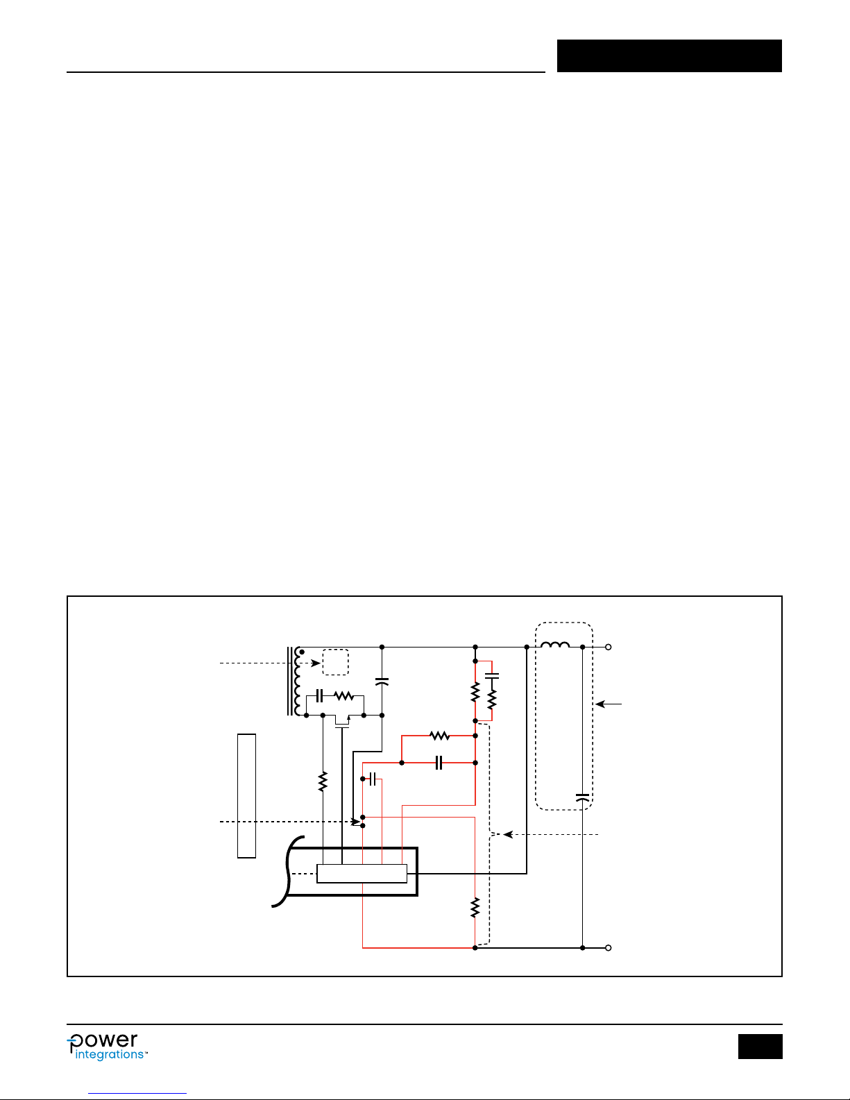
Application NoteAN-72
close as possible to the SOURCE and PRIMARY BYPASS pins of the
device.
Primary sensed OVP can be realized by connecting a series
combination of a Zener diode, a resistor and a blocking diode from
the rectied and ltered bias winding voltage supply to the PRIMARY
BYPASS pin (see Figure 18-a). The rectied and ltered bias winding
output voltage may be higher than expected (up to 1.5X or 2X the
desired value) dependent on the coupling of the bias winding with the
output winding and the resulting ringing on the bias winding voltage
waveform. It is therefore recommended that the rectied bias
winding voltage be measured. Ideally this measurement should be
made at the lowest input voltage and with full output load. This
measured voltage should be used to select the components required
to provided primary sensed OVP. It is recommended that a Zener
diode with a clamping voltage approximately 6 V lower than the bias
winding rectied voltage at which OVP is expected to be triggered be
used. A forward voltage drop of 1 V can be assumed for the blocking
diode. A small signal standard recovery diode should be used. The
blocking diode prevents any reverse current charging the bias
capacitor during start-up. Finally, the value of the series resistor set
such that a current higher than ISD will ow into the PRIMARY BYPASS
pin during an output overvoltage event.
Secondary-Side Overvoltage Protection
Secondary-side output overvoltage protection is provided by the
InnoSwitch3 IC. It is activated when an internal auto-restart is
triggered when a current exceeding the I
the SECONDARY BYPASS pin. The direct output sensed OVP function
threshold is fed into
BPS (SD)
can be realized by connecting a Zener diode from the output to the
SECONDARY BYPASS pin. The Zener diode voltage rating shall be the
difference between 1.25 V
voltage. It is necessary to add a low value resistor, in series with the
and 4.4 V SECONDARY BYPASS pin
OUT
OVP Zener diode to limit the maximum current into the SECONDARY
BYPASS pin (see Figure 18-b).
An OVP for a 5 V output can be implemented by two-diodes in series
(shown in Figure 18-c). The lter capacitor should be rated for 6.3 V.
Recommendations for Circuit Board Layout
Single-Point Grounding
Use a single-point ground connection from the input lter capacitor to
the area of copper connected to the SOURCE pin. See Figures 19 and
20.
Bypass Capacitors
The PRIMARY BYPASS (C
capacitors must be located directly adjacent to the PRIMARY
BYPASS-SOURCE, SECONDARY BYPASS-GROUND and FEEDBACKGROUND (CFB) pins respectively and connections should be routed via
short traces.
Signal Components
External components R
used for monitoring feedback information must be placed as close as
possible to the IC pin with short traces.
Critical Loop Area
Circuits where high dv/dt or di/dt occurs should be kept as small as
possible. The area of the primary loop that connects the input lter
capacitor, transformer primary and IC should be kept as small as
possible.
No loop area should be placed inside another loop (see Figure 21).
This will minimize cross-talk between circuits.
Primary Clamp Circuit
A clamp is used to limit peak voltage on the DRAIN pin at turn-off.
This can be achieved by using an RCD clamp or a Zener diode (~200 V)
and diode clamp across the primary winding. To reduce EMI, minimize
the loop between the clamp components, the transformer and the IC.
), SECONDARY BYPASS (C
BPP
, RBP, R
LS
FB(UPPER)
, R
FB(LOWER)
) decoupling
BPS
and RIS which are
L
Secondary loop area (4)
formed by NS, C
SR-FET must be tight
and small as possible
OUT
and
N
T
S
4
C
SR
R
SR
P
SR FET
C
OUT
R
FB(UPPER)
R
FB(LOWER)
C
FB
C
PH
R
PH
PF
V
OUT
If used, post filter L
CPF must be as close as
possible to output terminals
Note that Feedback network
(i.e. R
must be connected before the
post filter inductor L
FB(UPPER)
) and V
R
C
I
Single-point or Star-Ground
connection; Ground traces
for GND pin, C
Feedback components are
separated and star-connected
to a single point at RIS node
Figure 19. Typical Schematic of InnoSwitch3 Primary-Side Showing Critical Loops Areas, Critical Component Traces and Single-Point or Star Grounding.
OUT
, and
M
A
R
Y
R
FWD
FWD
BPS
GND
BPS
SR
IS
Secondary
Control IC
PI-8466a-111017
FB
VOUT
C
PF
Red lines denote the trace
must be as shorts as possible
and as close as possible to
IC pins
R
IS
RTN
PF
OUT
PF
and
pin
www.power.com
23
Rev. A 10/18
Page 24

Application Note AN-72
Y Capacitor
The placement of the Y capacitor should be directly from the primary
input lter capacitor positive terminal to the output positive or return
terminal of the transformer secondary. Such a placement will route
high magnitude common mode surge currents away from the IC.
Note that if an input pi EMI lter C1, LF, C2 is used, then the inductor
in the lter should be placed between the negative terminals of the
input lter capacitors.
Output SR MOSFET
For best performance, the area of the loop connecting the secondary
winding, the output SR MOSFET, and the output lter capacitor
should be minimized. In addition, sufcient copper area should be
provided at the terminals of the SR MOSFET for heat sinking. The
distance between SR FET source and InnoSwitch3 GROUND pin
needs to be short. To prevent negative current owing through the
primary MOSFET.
ESD Immunity
Sufcient clearance should be maintained (>8 mm) between the
primary-side and secondary-side circuits to enable easy compliance
, C1 and FB should be
L
F
positioned away from any
switching nodes with high
di/dt or dv/dt
Primary loop area (1) formed
by C2, N
and D-S pins must
P
be tight and small as possible
F
R
L
R
T
N
Single-point or star-ground
connection; ground traces
for bias supply and SOURCE
pin are separated and
connected to a single-point
at C2 node
O
t
BRD
C1
L
F
C2
F
B
with any ESD or hi-pot isolation requirements. The spark gap is best
placed between output return and/or positive terminals and one of
the AC inputs (after the fuse). In this conguration a 6.4 mm (5.5
mm is acceptable – dependent on customer requirement) spark gap
is more than sufcient to meet the creepage and clearance
requirements of most applicable safety standards. This is less than
the primary to secondary spacing because the voltage across spark
gap does not exceed the peak of the AC input. See layout example
Figure 21.
A spark gap across the common-mode-choke or inductor helps
provide low impedance path for a high energy discharge due to ESD
or a common-mode surge.
Drain Node
The drain switching node is the dominant noise generator. As such
the components connected the drain node should be placed close to
the IC and away from sensitive feedback circuits. The clamp circuit
components should be located physically away from the PRIMARY
BYPASS pin, and the trace width and length in this circuit should be
minimized.
PRIMARY
R
SNCSN
RSD
1
InnoSwitch3
Primary FET
and Controller
SN
2
C
BIAS
R
LS1
D V
S
R
C
BPP
BP
N
T
Primary clamp loop
P
area (2) must be tight
C
P
R
P
D
BIAS
3
and small as possible
Bias supply loop
area (3) must be tight
and small as possible
N
B
S
E
C
O
R
LS
N
D
A
R
Y
BPP
Red lines denote as short
as possible and as close
as possible to IC pins
PI-8467a-103017
Figure 20. Typical Schematic of InnoSwitch3 Secondary-Side Showing Critical Loops Areas, Critical Component Traces and Single-Point or Star Grounding.
Optional Post Filter LC included.
24
Rev. A 10/18
www.power.com
Page 25

Layout Example
Application NoteAN-72
Primary loop (1) formed
by C2, NP and D-S pin is
compact and small
Note that Drain trace is
short and narrow
Primary clamp loop
area (2) formed by
CSN, RS, DSN and
NP is compact and small
LF, C1 and FB are
positioned away from
any switching nodes
with high di/dt or dv/dt
Copper heat sink for
SOURCE pin is
maximized
Bias supply loop (3)
formed by NB, DBIAS and
CBIAS is compact and small
Special Notes
• All loops are separated; no loop is inside a loop. This will avoid ground impedance noise coupling.
• Keep trace surface area and length of high dv/dt nodes such as Drain, as small and short as possible to minimize RFI generation.
• No (quiet) signal trace such as Y capacitor and feedback return should be routed near to or across noisy nodes (high dv/dt or di/dt) such as Drain, underneath
transformer belly, switching-side of any winding or output rectier diode. This avoids capacitive or magnetic noise coupling.
• No signal trace should share path with traces having an AC switching current such as the output capacitors. Connection must be star-connected to capacitor
pad in order to avoid ground impedance coupled noise.
Optional Y capacitor
connected to RTN
and C1 (+)
5.5 mm spark-gap; primary-side
is connected directly to the AC input (after the fuse),
while secondary-side has one from RTN and VOUT
to increase effectiveness
1
3
Components CBPP, RBP, RLS1 and
RLS are placed as close as possible
to IC pin to which they are
connected to with short traces
5
No trace is routed
underneath the IC to
increase ESD immunity
4
PI-8522-091318
Output loop (5) formed
by CPF, RIS and COUT
does not share ground
path with secondary
loop (4)
Secondary loop (4)
formed by NS, COUT
and SR FET is compact
and small
Components CBPS,
CFB, RLS1, RFBLOWER
and GND pin share one
ground path that is
star-connected to RIS
All signal components
are placed as close as
possible to IC pin via
short traces
Figure 21. TOP and BOTTOM Sides – Ideal Layout Example Showing Tight Loop Areas for Circuit with High dv/dt or di/dt, Component Placement and Spark-Gap
Location in Reference to Figures 19 and 20.
www.power.com
25
Rev. A 10/18
Page 26

Application Note AN-72
Output
Terminals
AC Input
Safety
Y Capacitor
Fuse
Input Filter
Capacitors
Thermistor
EMI Filter
Inductor
AC Input
Figure 22. TOP Side – Layout Example Showing Through-Hole Components.
Output
Capacitor
Transformer
PI-8521-103117
26
Rev. A 10/18
www.power.com
Page 27

Application NoteAN-72
Recommended Position of InSOP-24D Package
with Respect to Transformer
The PCB underneath the transformer and InSOP-24D must be rigid.
If a large size transformer core is used on the board with thin PCB,
(<1.5 mm), it is recommended that the transformer be away from the
Force
Transformer
Supporting
Stand-Off
InSOP-24D
Supporting
Stand-Off
PI-8523-020618
InSOP package. Cutting a slot in the PCB that runs near to or
underneath the InSOP package is generally not recommended as this
weakens the PCB. In the case of a long PCB, it is recommended that
mechanical support or post be placed in the middle of the board or
near the InSOP package.
Slot not
recommended
(23-a)
Force
Transformer
Supporting
Stand-Off
(23-c)
Figure 23. Recommended Position of InSOP-24D Package Shown with Check Mark.
InSOP-24D
Supporting
Stand-Off
PI-8524-020618
(23-b)
Supporting
Stand-Off
(23-d)
Transformer
Force
InSOP-24D
Supporting
Stand-Off
PI-8525-042618
www.power.com
27
Rev. A 10/18
Page 28

Application Note AN-72
Recommendations to Reduce No-load Consumption
The InnoSwitch3 IC will start in self-powered mode, drawing energy
from the BYPASS pin capacitor that is charged from an internal
current source. A bias winding is required to provide supply current
to the PRIMARY BYPASS pin once the InnoSwitch3 IC has started
switching. A bias winding supply to the PRIMARY BYPASS pin enables
power supplies with no-load power consumption of less than 15 mW.
Resistor RBP shown in Figure 13 should be adjusted to achieve the
lowest no-load input power.
Other areas that may help reduce no-load consumption further are;
1. Low value of primary clamp capacitor, CSN.
2. Schottky or ultrafast diode for bias supply rectier, D
3. Low ESR capacitor for bias supply lter capacitor, C
4. Low value SR FET RC snubber capacitor, CSR.
BIAS
BIAS
.
.
5. Tape between primary winding layers, and multi-layer tapes
between primary and secondary windings to reduce inter
winding capacitance.
Recommendations for Reducing EMI
1. Appropriate component placement and small loop areas of the
primary and secondary power circuits help minimize radiated
and conducted EMI. Care should be taken to achieve a compact
loop area. (See Figures 19 and 20)
2. A small capacitor parallel to the clamp diode on the primary-side
can help reduce radiated EMI.
3. A resistor (2 – 47 Ω) in series with the bias winding helps reduce
radiated EMI.
4. A small resistor and ceramic capacitor (< 22 pf) in series across
primary shown in Figure 20 and/or across secondary winding
(< 100 pf) may help reduce conducted and/or radiated EMI.
However if value is large, then no-load consumption will
increase.
5. Common mode chokes are typically required at the input of the
power supply to sufciently attenuate common-mode noise.
However, the same performance can be achieved by use of
shield windings in the transformer. Shield windings can also be
used in conjunction with common mode lter inductors at the
input to reduce conducted and radiated EMI.
6. Adjusting SR MOSFET RC snubber component values can help
reduce high frequency radiated and conducted EMI.
7. A pi lter comprising differential inductors and capacitors can be
used in the input rectier circuit to reduce low frequency
differential EMI. A ferrite bead as shown in Figure 20 can be
added to further improve EMI margin at minimal cost.
8. A resistor across the differential inductors reduces their Q factor
which can reduce EMI above 10 MHz. However low frequency
EMI below 5 MHz may increase slightly.
9. A 1 µF ceramic capacitor connected at the output of the power
supply may help to reduce radiated EMI.
10. A slow diode (i.e. 250 ns < t
(D
) is generally good for reducing conducted EMI > 20 MHz
BIAS
and radiated EMI
< 500 ns) as the bias rectier
RR
> 30 MHz.
Recommendations for Increased ESD Immunity
1. Sufcient clearance should be maintained (> 8 mm) between the
primary-side and secondary-side circuits (especially underneath
InSOP package and transformer).
a. It is not recommended to place spark gap near or
across InSOP package.
2. Use two spark gaps connected to secondary terminals (output
return and positive) and one of the AC inputs after the fuse
(see Figure 21). In this conguration at least 5.4 mm gap is
often sufcient to meet creepage and clearance requirements of
applicable safety standards.
a. For applications with a USB connector, oat the PCB pads
connected to the legs of the connector.
3. Use a spark gap across common-mode choke or inductor to
provide a low impedance path for any high energy discharge
build up due to ESD or common mode surge.
4. Use a Y capacitor connected from either positive or negative
output terminals to the input bulk capacitor’s positive terminal or
to the AC input after the fuse.
5. Employ good layout practices and follow the PCB layout
recommendations in the application note.
6. Apply multi-layer tape between bias and secondary windings,
and also between secondary and primary windings.
Thermal Management Considerations
The SOURCE pin is internally connected to the IC lead frame and
provides the main path to remove heat from the device. Therefore
the SOURCE pin should be connected to a copper area underneath
the IC to act not only as a single point ground, but also as a heat
sink. As this area is connected to the quiet source node, it can be
maximized for good heat sinking without causing EMI proplems.
Similarly for the output SR MOSFET, maximize the PCB area
connected to the pins on the package through which heat is
dissipated.
Sufcient copper area should be provided on the board to keep the
IC temperature safely below absolute maximum limits. It is
recommended that the copper area to which the SOURCE pin of the
IC is soldered is sufciently large to keep the IC temperature below
90 °C when operating the power supply at full rated load and at the
lowest rated input AC supply voltage (at nominal ambient). Further
de-rating can be applied as required.
Heat Spreader
For stringent thermal requirements, position the IC adjacent to the
transformer as shown in Figure 23-d. This will reduce heat transfer
to the IC from the transformer. For enclosed high power applications
such as laptop adaptor or similar applications with high ambient
environment, using the PCB as a heat sink may not be enough for the
IC to operate within specied operating temperature, therefore a
metal heat spreader may be necessary to keep the IC cool. Unless a
ceramic material is used for the heat sink, care must be taken to
maximize the safety limit. A heat spreader is formed by combination of
a heat spreader material (Copper or Aluminum), a 0.4 mm mylar pad
(for reinforced isolation) and a thermally conductive pad for better
heat transfer between the IC and the spreader.
Figure 24 shows the basic idea how to implement the attachment of a
heat spreader to an InSOP-24D package while maintaining creepage
between primary-side and secondary-side pins of InnoSwitch3 IC.
28
Rev. A 10/18
www.power.com
Page 29

Application NoteAN-72
d > 6.6 mm
Mylar 0.4 mm
Mylar 0.4 mm
d > 6.6 mm
Thermal Pad
d > 6.6 mm
6.6 mm
InSOP-24D
Heat Sink
0.5 mm
InSOP-24D
d ~ 4.2 mm
Heat Sink
Power
FET
Thermal Pad
0.4 mm
Secondary
Control
InSOP-24D
Figure 24. Simplied Diagram of Heat Spreader Attachment to an InSOP-24D Package.
Quick Design Checklist
As with any power supply, the operation of all InnoSwitch3 designs
should be veried on-the-bench to make sure that component limits
are not exceeded under worst-case conditions. As a minimum, the
following tests are strongly recommended:
Maximum Drain Voltage
Verify that V
breakdown voltages at the highest input voltage and peak (overload)
output power in normal operation and during start-up.
Maximum Drain Current
At maximum ambient temperature, maximum input voltage and peak
output (overload) power. Review Drain current waveforms for any
of InnoSwitch3 and SR FET do not exceed 90% of
DS
spikes at start-up. Repeat tests under steady-state conditions and
verify that the leading edge current spike is below I
of t
primary MOSFET should be below the specied absolute maximum
ratings.
Thermal Check
At specied maximum output power, minimum input voltage and
maximum ambient temperature. Verify that temperature specication
limits for InnoSwitch3 IC, transformer, output SR FET, and output
capacitors are not exceeded. Enough thermal margin should be
allowed for part-to-part variation of MOSFET R
maximum power, a maximum InnoSwitch3 SOURCE pin temperature
of 110 °C is recommended to allow for R
signs of transformer saturation or excessive leading-edge current
Primary
Control
4.2 mmInnoSwitch3
PI-8377-020918
. Under all conditions, the maximum Drain current for the
LEB(MIN)
DS(O N)
LIMIT(MIN)
. At low-line,
DS(O N)
variation.
at the end
www.power.com
29
Rev. A 10/18
Page 30

Application Note AN-72
Simple Circuit Ideas
Line OV Only
Diode biased from BPP and provides
constant current into the VOLTAGE pin via
R2 above IUV threshold, thus disabling UV
function of the IC.
Line UV Only
Zener clamps the voltage on R1-R2 node
and provides constant voltage above I
thresholds, thus disabling OV function of
UV
the IC.
+
+
6.2 V
1N4148
R1
R2
D V
S IS
BPP
FWD
InnoSwitch3-CE
R1
R2
D V
S IS
BPP
FWD
InnoSwitch3-CE
SR
SR
GND
GND
BPS
FB
VOUT
PI-8403-081617
BPS
FB
VOUT
Fast AC Reset for IC with OV Latch
Function
Diode allows VOLTAGE pin to monitor line
voltage for OV/UV detection. A capacitor is
sized to lter the line ripple. CS must be
small to allow the VOLTAGE pin to
discharge fast enough to go below the
I
threshold in order to reset the latch.
UV-
Figure 25. Circuit Ideas to Enhance Design.
Diode
Cap
C
100 nF
PI-8404-081617
R2
D V
S
S IS
BPP
FWD
SR
GND
BPS
FB
VOUT
InnoSwitch3
PI-8468-100417
30
Rev. A 10/18
www.power.com
Page 31

RC Network Across RFB
In some applications where low output
UPPER
ripple voltage is required, it is necessary to
speed up the feedback sensing by adding
an RC phase-boost network circuit in
parallel with upper feedback resistor. A
good starting value is 1 nF and 1 kΩ.
InnoSwitch3
Primary FET
and Controller
SR FET
D V
S IS
BPP
FWD
SR
Diode
Application NoteAN-72
GND
BPS
FB
Secondary
Control IC
PI-8473-100417
C
R
VOUT
F
F
R
IS
Diode Across SR FET
Putting a Schottky diode across the SR FET
may further increase efciency by 0.1 to
0.2% depending on the input and the
SR FET used.
Capacitor Across OUTPUT VOLTAGEGROUND Pins
Putting a small ceramic capacitor (up to
10 µF) from OUTPUT VOLTAGE to
GROUND pins can reduce output ripple
InnoSwitch3
Primary FET
and Controller
InnoSwitch3
Primary FET
and Controller
SR FET
D V
S IS
D V
S IS
BPP
BPP
FWD
FWD
SR
SR
GND
BPS
FB
Secondary
Control IC
PI-8470-100417
GND
BPS
FB
Secondary
Control IC
C
VOUT
VOUT
VOUT
R
IS
R
IS
Figure 25 (cont.). Circuit Ideas to Enhance Design.
www.power.com
PI-8472-100417
31
Rev. A 10/18
Page 32

Application Note AN-72
PI-8544-111017
Diode Across Current Sense RIS
A diode (Schottky or ultrafast) positioned
across the current sense resistor (RIS) acts
as a bypass for very high surge of current
and voltage during short-circuit which
could potentially damage RIS. This is more
likely for designs with high output voltage
and high output lter capacitance.
InnoSwitch3
Primary FET
and Controller
D V
S IS
BPP
FWD
SR
GND
BPS
FB
Secondary
Control IC
PI-8469-101017
VOUT
R
IS
Diode
Capacitor Across Current Sense RIS
Putting a capacitor (10 - 100 nF) across IS
and GND pins when RIS is placed somewhat away from the IC will reduce pulse
grouping (bunching) in CC operation.
Figure 25 (cont.). Circuit Ideas to Enhance Design.
InnoSwitch3
Primary FET
and Controller
D V
S IS
BPP
FWD
SR
GND
BPS
FB
VOUT
Secondary
Control IC
C
R
IS
GS
32
Rev. A 10/18
www.power.com
Page 33

Application Examples
C6
680 pF
250 VAC
Application NoteAN-72
1
FL1
L1
15 mH
L
TP1
R1
1.5 MΩ
F1
3.15 A
1
2 3
C1
220 nF
275 VAC
90 - 265
VAC
4
R2
2 MΩ
RT1
2.5 Ω
BR1
GBU4J-BP
600 V
N
TP2
C3
R3
2.2 nF
100 kΩ
630 V
R6
49.9 kΩ
1%
1/8 W
R4
47 Ω
2 W
R7
1.80 MΩ
1%
R8
1.80 MΩ
C2
120 µF
400 V
O
t
1%
D1
FR107G
D2
DFLR1200-7
200 V
R5
5.1 kΩ
1/10 W
C4
22 µF
50 V
6
2
9
3
T1
PQ26/20
InnoSwitch3-CE
INN3168C-H101
R9
47 Ω
1/10 W
FWD
U1
12 Ω
R11
NC
4
5
D
D V
CONTROL
S
S IS
BPP
C5
4.7 µF
50 V
Figure 26. Schematic of DER-535 65 W, 19 V Power Supply using INN3168C.
A High Efciency, 65 W Universal Input Power Supply
(InnoSwitch3-CE)
The circuit shown in Figure 26 delivers 65 W (19 V at 3.4 A) at higher
than 90% average efciency from 90 VAC to 265 VAC input using
INN3168 C.
The bleeding resistors, R1 and R2, are used to discharge the stored
energy in C1 to meet safety requirement. The input capacitor C2 is
sufcient to maintain full output power delivery at 90 VAC input, and
Resistors R6, R7, and R8 provide line voltage sensing. At
approximately 100 V DC, the current through these resistors exceeds
the line undervoltage threshold, which enables U1. At approximately
420 V DC, the current through these resistors exceeds the line
overvoltage threshold, disabling U1. A low cost RCD clamp formed by
D1, R3, R4, and C3 limits the peak drain voltage due to the interaction
of transformer leakage reactance with output trace inductance.
C10
2.2 nF
250 V
Q1
AO4294
SR
R13
143 kΩ
1%
C11
560 µF
35 V
C8
10 nF
C7
2.2 µF
25 V
BPS
VO
GND
FB
1/8 W
R14
10 kΩ
1%
1/16 W
C9
330 pF
50 V
VR1
MMSZ5232B-7-F
R10
0.007 Ω
1%
1/2 W
C12
560 µF
35 V
D3
DFLR1200-7
200 V
1/10 W
R12
100 Ω
L2
155 µH
1 4
2 3
PI-8430-082018
C14
1 µF
100 V
The secondary-side of the INN3168C provides output voltage and
output current sensing, and provides drive to a synchronous
rectication MOSFET. Output rectication for the 19 V output is
provided by SR FET Q1. Very low ESR capacitors, C11 and C12,
provide ltering. RC snubber network comprising R11 and C10 for Q1
damps high frequency ringing across the SR FET, which results from
leakage of the transformer windings and the secondary trace.
Capacitor C8 protects U1 from ESD. Adding a small SMD ceramic
capacitor between the OUTPUT VOLTAGE pin and the GROUND pin
improves ESD and surge protection. The OVP sensing Zener diode,
VR1, provides secondary-side output over voltage protection via R12.
Output common mode choke L2 reduces high frequency common
mode noise and protects U1 from common mode surge.
A heat spreader is required to keep the InnoSwitch3 device below
110 °C when operating under full load, low-line, while at maximum
ambient temperature.
19 V, 3.4 A
TP3
RTN
www.power.com
33
Rev. A 10/18
Page 34

Application Note AN-72
C10
470 pF
BR1
DF08S
800 V
F1
1 A
RT1
10 Ω
90 - 265
VAC
L N
250 VAC
21FL1
CONTROL
BPP
4.7 µF
4
3
C6
16 V
FL2
6
5
NC
T1
EE1621
InnoSwitch3-EP
INN3672C-H602
R9
47 Ω
1/10 W
FWD
R24
62 Ω
1/8 W
U1
R3
2 MΩ
1%
R4
1.8 MΩ
1%
C3
C2
10 µF
10 µF
400 V
400 V
O
t
DFLR1200-7
L1
330 µH
C4
R8
1000 pF
200 kΩ
630 V
D1
R22
DFLR1600-7
68 Ω
600 V
D7
C5
22 µF
50 V
D3
BAV21WS-7-F
1/10 W
VR1
MMSZ5231B-7-F
R6
6.2 kΩ
D V
R26
36 Ω
1/10 W
S IS
AO4486
C22
1 nF
200 V
Q1
AO6420
SR
C21
1 nF
200 V
Q2
R25
30 Ω
1/8 W
2.2 µF
VO
C19
680 µF
16 V
C18
560 µF
6.3 V
C7
25 V
BPS
C8
330 pF
50 V
GND
FB
R29
100 Ω
1/10 W
C23
2.2 nF
50 V
R30
100 Ω
1/10 W
C24
2.2 nF
50 V
R16
133 kΩ
1%
1/16 W
R13
33.2 kΩ
1%
1/16 W
R12
0.2 Ω
1%
R27
1.2 MΩ
1%
1/16 W
10 µH
10 µH
L2
L3
VR2
SMAZ8V2-13-F
8.2 V
C12
2.2 µF
25 V
PI-8374-082018
C14
2.2 µF
25 V
12 V, 0.7 A
5 V, 0.3 A
RTN
Figure 27. Schematic DER-611, 5 V, 0.3 A and 12 V, 0.7 A for HVAC (Heating, Ventilation and Air-Conditioning) Application.
A High Efciency, 10 W, Dual Output – Universal Input Power
Supply (InnoSwitch3-EP)
The circuit in Figure 27 delivers 10 W output power from 90 VAC to
265 VAC input. Higher than 84% efciency at 90 VAC input at full
load is achieved (using INN3672C from the InnoSwitch3-EP family), and
provides accurate cross regulation between two outputs with two SR
FETs.
Primary-side overvoltage protection is obtained using Zener diode
VR1. In the event of overvoltage occurred on any output, the
increased voltage at the output of the bias winding causes the Zener
diode VR1 to conduct and triggers the OVP latch in the primary-side
controller of the InnoSwitch3-EP IC.
Output rectication of the 5 V output is provided by SR FET Q1, and
output rectication of the 12 V output is provided by SR FET Q2. The
timing of Q1 and Q2 turn-on is controlled by the 5 V winding voltage
sensed via R9 and the FORWARD pin of the IC. Resistor R16, R27
and R13 form a voltage divider network that senses the output
voltage from both outputs to provide better cross-regulation. The
feedback current ratio between 12 V and 5 V outputs is 1:3 to provide
better regulation on the 5 V output and good cross regulation.
Feedback compensation networks comprising capacitors C23 and C24
reduce output ripple voltage. Capacitor C8 provides decoupling to
prevent high frequency noise interfering with power supply operation.
Zener diode VR2 improves the cross regulation when the 5 V output
only is fully loaded when no-load is present on the 12 V output.
34
Rev. A 10/18
www.power.com
Page 35

Notes
Application NoteAN-72
www.power.com
35
Rev. A 10/18
Page 36

Revision Notes Date
A Initial release. 10/18
For the latest updates, visit our website: www.power.com
Power Integrations reserves the right to make changes to its products at any time to improve reliability or manufacturability. Power Integrations
does not assume any liability arising from the use of any device or circuit described herein. POWER INTEGRATIONS MAKES NO WARRANTY
HEREIN AND SPECIFICALLY DISCLAIMS ALL WARRANTIES INCLUDING, WITHOUT LIMITATION, THE IMPLIED WARRANTIES OF MERCHANTABILITY,
FITNESS FOR A PARTICULAR PURPOSE, AND NON-INFRINGEMENT OF THIRD PARTY RIGHTS.
Patent Information
The products and applications illustrated herein (including transformer construction and circuits external to the products) may be covered by one
or more U.S. and foreign patents, or potentially by pending U.S. and foreign patent applications assigned to Power Integrations. A complete list of
Power Integrations patents may be found at www.power.com. Power Integrations grants its customers a license under certain patent rights as set
forth at www.power.com/ip.htm.
Life Support Policy
POWER INTEGRATIONS PRODUCTS ARE NOT AUTHORIZED FOR USE AS CRITICAL COMPONENTS IN LIFE SUPPORT DEVICES OR SYSTEMS
WITHOUT THE EXPRESS WRITTEN APPROVAL OF THE PRESIDENT OF POWER INTEGRATIONS. As used herein:
1. A Life support device or system is one which, (i) is intended for surgical implant into the body, or (ii) supports or sustains life, and (iii) whose
failure to perform, when properly used in accordance with instructions for use, can be reasonably expected to result in signicant injury or
death to the user.
2. A critical component is any component of a life support device or system whose failure to perform can be reasonably expected to cause the
failure of the life support device or system, or to affect its safety or effectiveness.
Power Integrations, the Power Integrations logo, CAPZero, ChiPhy, CHY, DPA-Switch, EcoSmart, E-Shield, eSIP, eSOP, HiperPLC, HiperPFS,
HiperTFS, InnoSwitch, Innovation in Power Conversion, InSOP, LinkSwitch, LinkZero, LYTSwitch, SENZero, TinySwitch, TOPSwitch, PI, PI Expert,
SCALE, SCALE-1, SCALE-2, SCALE-3 and SCALE-iDriver, are trademarks of Power Integrations, Inc. Other trademarks are property of their
respective companies. ©2018, Power Integrations, Inc.
Power Integrations Worldwide Sales Support Locations
World Headquarters
5245 Hellyer Avenue
San Jose, CA 95138, USA
Main: +1-408-414-9200
Customer Service:
Worldwide: +1-65-635-64480
Americas: +1-408-414-9621
e-mail: usasales@power.com
China (Shanghai)
Rm 2410, Charity Plaza, No. 88
North Caoxi Road
Shanghai, PRC 200030
Phone: +86-21-6354-6323
e-mail: chinasales@power.com
China (Shenzhen)
17/F, Hivac Building, No. 2, Keji Nan
8th Road, Nanshan District,
Shenzhen, China, 518057
Phone: +86-755-8672-8689
e-mail: chinasales@power.com
Germany (AC-DC/LED Sales)
Lindwurmstrasse 114
D-80337 München
Germany
Phone: +49-89-5527-39100
e-mail: eurosales@power.com
Germany (Gate Driver Sales)
HellwegForum 1
59469 Ense
Germany
Tel: +49-2938-64-39990
e-mail: igbt-driver.sales@power.com
India
#1, 14th Main Road
Vasanthanagar
Bangalore-560052 India
Phone: +91-80-4113-8020
e-mail: indiasales@power.com
Italy
Via Milanese 20, 3rd. Fl.
20099 Sesto San Giovanni (MI) Italy
Phone: +39-024-550-8701
e-mail: eurosales@power.com
Japan
Yusen Shin-Yokohama 1-chome Bldg.
1-7-9, Shin-Yokohama, Kohoku-ku
Yokohama-shi,
Kanagawa 222-0033 Japan
Phone: +81-45-471-1021
e-mail: japansales@power.com
Korea
RM 602, 6FL
Korea City Air Terminal B/D, 159-6
Samsung-Dong, Kangnam-Gu,
Seoul, 135-728, Korea
Phone: +82-2-2016-6610
e-mail: koreasales@power.com
Singapore
51 Newton Road
#19-01/05 Goldhill Plaza
Singapore, 308900
Phone: +65-6358-2160
e-mail: singaporesales@power.com
Taiwan
5F, No. 318, Nei Hu Rd., Sec. 1
Nei Hu Dist.
Taipei 11493, Taiwan R.O.C.
Phone: +886-2-2659-4570
e-mail: taiwansales@power.com
UK
Building 5, Suite 21
The Westbrook Centre
Milton Road
Cambridge
CB4 1YG
Phone: +44 (0) 7823-557484
e-mail: eurosales@power.com
 Loading...