Power Innovations TISPPBL2SDR, TISPPBL2SD Datasheet

TISPPBL2SD
‡ C
SLIC inf
K1
PROGRAMMABLE OVERVOLTAGE PROTECTORS
FOR ERICSSON COMPONENTS PBL 3xxx SLICS
AUGUST 1999Copyright © 1999, Power Innovations Limited, UK
OVERVOLTAGE PROTECTION FOR ERICSSON COMPONENTS LINE INTERFACE CIRCUITS
Overvoltage Protector‡ for:-
●
PBL 3762A
PBL 3764A/4, PBL 3764A/6
PBL 3766, PBL 3766/6
PBL 3767, PBL 3767/6
PBL 3796, PBL 3796/2
PBL 3798, PBL 3798/2
PBL 3798/5
PBL 3798/6
PBL 3799
PBL 3860A/1, PBL 3860A/6
PBL 386 10/2
PBL 386 11/2
PBL 386 20/1
PBL 386 21/1
PBL 386 30/1
PBL 386 40/1
PBL 386 50/1
PBL 3898/M
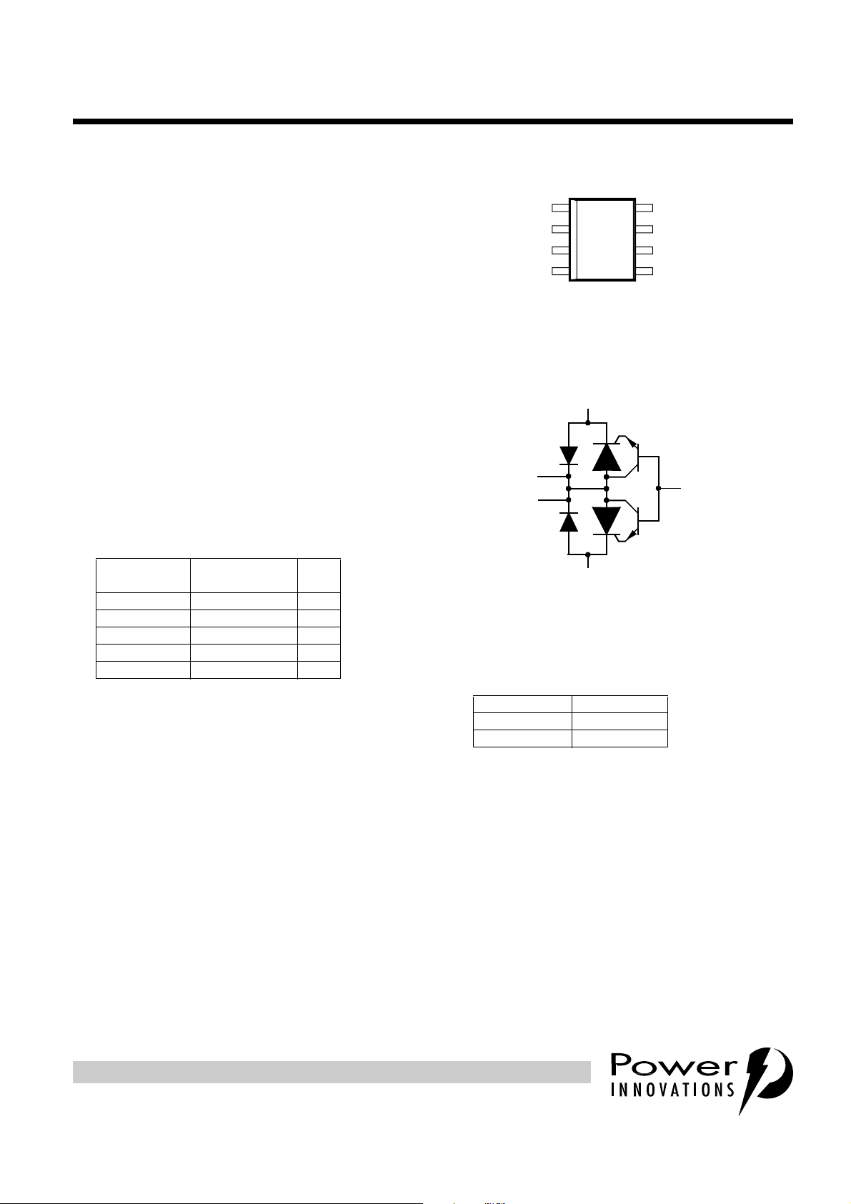
(Tip)
(Gate)
(Ring)
Terminal typical application names shown in
device symbol
A
A
D PACKAGE
(TOP VIEW)
K1
G
NC
K2
NC - No internal connection
1
2
3
4
parenthesis
8
7
6
5
NC
A
A
NC
(Ground)
(Ground)
MD6XBA
G1,G2
Rated for International Surge Wave Shapes
●
I
WAVE SHAPE STANDARD
2/10 µs GR-1089-CORE 100
1.2/50 µs ITU-T K22 100
0.5/700 µs I3124 40
10/700 µs ITU-T K20, K21 40
10/1000 µs GR-1089-CORE 30
Single-Lead Line Connection Version of
●
Feed-Through TISPPBL2D
- Ground Lead Creepage Distance . . > 3 mm
TSP
A
K2
Termin als K1, K2 and A cor respond to t he alternative
line designators of T, R and G or A, B and C. The
negative protection voltage is controlled by the
voltage, V
Small Outline Surface Mount Package
●
applied to the G terminal.
GG,
- Available Ordering Options
CARRIER ORDER #
Tube TISPPBL2SD
Taped and reeled TISPPBL2SDR
description
The TISPPBL2S is a dual forward-conducting buffered p-gate overvoltage protector. It is designed to p rotect
the Ericsson Components PBL 3xxx family of SLICs (Subscriber Line Interface Circuits) against overvoltages
on the telephone line cause d by lightning, a.c. power contact and indu ction. The TISPPB L2S limits voltages
that exceed the SLIC supply rail levels.
The SLIC line driver section is typically powered from 0 V (ground) and a negative voltage in the region of
-10 V to -85 V. The protector gate is connected to this negative supply. This references the protection
(clipping) voltage to the negative supply voltage. As the protection voltage will track the negative supply
voltage the overvoltage stress on the SLIC is minimised.
SD6XAP
Positive overvoltage s are clipped to grou nd by diode forward conduction. Negative overvoltage s are initially
clipped close to the SLIC negative supply rail value. If sufficient current is available from the overvoltage, then
the protector will crowbar into a low voltage ground referenced on-state condition. As the overvoltage
ustomers are advised to obtain the latest version of the relevant Ericsson Components
the information being relied on is current.
ormation to verify, before placing orders, that
PRODUCT INFORMATION
Information is current as of publication date. Products conform to specifications in accordance
with the terms of Power Innovations standard warranty. Production processing does not
necessarily include testing of all parameters.
1

TISPPBL2SD
PROGRAMMABLE OVERVOLTAGE PROTECTORS
FOR ERICSSON COMPONENTS PBL 3xxx SLICS
AUGUST 1999
subsides the high holdin g c ur rent of th e cr owbar prevents d.c. latchup. The TISPPBL2S buffered gate design
reduces the loading on the SLIC supply during overvoltages caused by power cross and induction.
These monolithic prote ction devices are fabricated in ion-implanted planar vertical power str uctures for high
reliability and in nor mal system operatio n they are virtual ly transparent. The TISPPBL2 S is the TISPPBL2D
with a different pinout. The feed-through Ring ( leads 4 — 5) and Tip (lead s 1 — 8) connections have been
replaced by single Ring (lea d 4) and Tip ( lead 1) connec tions. This in creases pa ckage creepag e distance of
the biased to ground connections from about 0.7 mm to over 3 mm.
absolute maximum ratings
RATING SYMBOL VALUE UNIT
≤
Repetitive peak off-state voltage, I
Repetitive peak gate-cathode voltage, V
Non-repetitive peak on-state pulse current (see Notes 1 and 2)
10/1000 µs (Bellcore GR-1089-CORE, Issue 1, November 1994, Section 4) 30
0.2/310 µs (I3124, open-circuit voltage wave shape 0.5/700µs)
5/310 µs (ITU-T K20 & K21, open-circuit voltage wave shape 10/700 µs)
1/20 µs (ITU-T K22, open-circuit voltage wave shape 1.2/50 µs)
2/10 µs (Bellcore GR-1089-CORE, Issue 1, November 1994, Section 4) 100
Non-repetitive peak on-state current, 50/60 Hz (see Notes 1 and 2)
100 ms 11
1s
5s
300 s
900 s
Non-repetitive peak gate current, 1/2 µs pulse, cathodes commoned (see Note 1) I
Operating free-air temperature range T
Junction temperature T
Storage temperature range T
= 0, -40°C≤T
G
= 0, -40°C≤T
KA
85°C V
J
≤
85°C V
J
DRM
GKRM
I
TSP
I
TSM
GSM
A
J
stg
-100 V
-90 V
40
40
100
4.5
2.4
0.95
0.93
40 A
-40 to +85 °C
-40 to +150 °C
-40 to +150 °C
A
A
NOTES: 1. Initially the protector must be in thermal equilibrium with -40 °C≤T
its initial conditions.
2. These non-repetitive rated currents are peak values for either polarirty. The rated current values may be applied either to the Ring
to Ground or to the Tip to Ground terminal pairs. Additionally, both terminal pairs may have their rated current values applied
simultaneously (in this case the Ground terminal current will be twice the rated current value of an individual terminal pair). Above
85 °C, derate linearly to zero at 150 °C lead temperature.
recommended operating conditions
C
G
R
1
electrical characteristics, T
I
D
Gate decoupling capacitor 100 220 nF
TISPPBL2S series resistor for GR-1089-CORE first-level and second-level surge survival
TISPPBL2S series resistor for GR-1089-CORE first-level surge sur vival
TISPPBL2S series resistor for ITU-T recommendation K20/21
= 25 °C (unless otherwise noted)
amb
PARAMETER TEST CONDITIONS MIN TYP MAX UNIT
Off-state current VD=V
DRM
, VGK=0
PRODUCT INFORMATION
≤
85 °C. The surge may be repeated after the device returns to
J
MIN TYP MAX UNIT
40
25
10
T
= -40 °C -5 µA
J
= 85 °C -50 µA
T
J
Ω
2

TISPPBL2SD
PROGRAMMABLE OVERVOLTAGE PROTECTORS
FOR ERICSSON COMPONENTS PBL 3xxx SLICS
AUGUST 1999
electrical characterist ics, T
PARAMETER TEST CONDITIONS MIN TYP MAX UNIT
I
V
t
(BR)
V
V
t
FR
I
H
I
GAS
I
GAT
I
GAF
I
GT
V
C
(BO)
F
FRM
GT
AK
Breakover voltage
Breakdown time
Forward voltage IF= 5 A, tw= 500 µs 3V
Peak forward recovery
voltage
Forward recovery time
Holding current IT= -1 A, di/dt = 1A/ms, VGG=-50V, -40°C≤T
Gate reverse current VGG=V
Gate reverse current,
on state
Gate reverse current,
forward conducting
state
Gate trigger current IT=-5A, t
Gate trigger voltage IT=-5A, t
Anode-cathode offstate capacitance
T
Figure 2)
I
T
cuit (See Note 3 and Figure 2)
IF= 20 A, 0.5/700 generator, Fi gure 3 test circuit (See Note 4 and Figure 2)
I
F
cuit (See Note 4 and Figure 2)
I
T
I
F
f=1MHz, V
= 25 °C (unless otherwise noted) (continued)
amb
= -20 A, 0.5/700 generator, Figure 3 test circuit (See Note 3 and
= -20 A, 0.5/700 generator, Figure 3 test cir-
< -50 V 1 µs
V
(BR)
-70 V
8V
10000
1
µs
= 20 A, 0.5/700 generator, Figure 3 test cir-
, VAK=0
GKRM
VF > 5 V
> 1 V
V
F
≤
85 °C -150 mA
J
T
= -40 °C -5 µA
J
T
= 85 °C -50 µA
J
=-0.5A, tw= 500 µs, VGG=-50V -1 mA
= 1 A, tw= 500 µs, VGG= -50 V -10 mA
≥
20 µs, V
p(g)
≥
20 µs, V
p(g)
=1V, IG= 0, (see Note 5)
d
=-50V 5 mA
GG
=-50V 2.5 V
GG
V
= -3 V 110 pF
D
V
=-50V 60 pF
D
NOTES: 3. For the required TIPX and RINGX terminal negative pulse performance refer to the respective Ericsson Components SLIC data
sheet. The PBL 379x family of SLICs has ratings of -120 V for 0.25 µs, -90 V for 1 µs, -70 V for 10 ms and -70 V for d.c. The PBL
376x family together with the PBL 3860A SLIC have the same maximum ratings when the applied battery voltage is -50V. As the
FLEXI-SLIC™ PBL 386 xx family is specified in terms of current pulses, a minimum value of 2Ω for R
Compliance to these conditions is guaranteed by the maximum breakover voltage and the breakdown times of the TISPPBL2S.
should be used.
P
4. For the required TIPX and RINGX terminal positive pulse performance refer to the respective Ericsson Components SLIC data
sheet. The PBL 379x family of SLICs has ratings of 15 V for 0.25 µs, 10 V for 1µs, 5 V for 10 ms and 1 V for d.c. The PBL 376x
family together with the PBL 3860A SLIC have similar ratings. As the FLEXI-SLIC™ PBL 386 xx family is specified in terms of
current pulses, a minimum value of 2Ω for R
should be used. Compliance to these conditions is guaranteed by the peak forward
P
recovery voltage and the forward recov ery times of the TISPPBL2S
5. These capacitance measurements employ a three terminal capacitance bridge incorporating a guard circuit. The unmeasured
device terminals are a.c. connected to the guard terminal of the bridge.
thermal characteristics
PARAMETER TEST CONDITIONS MIN TYP MAX UNIT
P
=0.8W, TA=25°C
R
Junction to free air thermal resistance
θ
JA
tot
5cm
2
, FR4 PCB
D Package 160 °C/W
PRODUCT INFORMATION
3

TISPPBL2SD
PROGRAMMABLE OVERVOLTAGE PROTECTORS
FOR ERICSSON COMPONENTS PBL 3xxx SLICS
AUGUST 1999
PARAMETER MEASUREMENT INFORMATION
V
GK(BO)
-v
I
(BO )
V
V
(BO)
Quad r a nt III
Switchin g
Characteristic
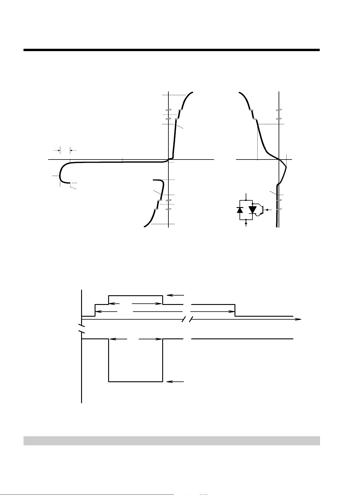
Figure 1. PRINCIPAL TERMINAL AND GATE TRANSFER CHARACTERISTICS
PRINCIPAL TERMINAL V-I CHARACTERISTIC
(= |I
I
FSP
I
(= |I
FSM
TSM
GG
I
S
V
S
V
D
V
T
TSP
GATE TRANSFER
CHARACTERISTIC
+i
|)
Quadrant I
Forward
Conduction
Characteristic
+i
K
|)
I
F
V
F
+v
-i
PM6XAIA
G
I
GAF
I
GAT
I
K
I
D
I
H
I
T
I
TSM
I
TSP
-i
I
F
I
GT
+i
G
I
T
I
G
-i
K
PROTECTOR MAXIMUM LIMIT ING VOLTAGE
vs
TIME
-50
VOLTAGE - V
-60
-70
-80
10
5
1 µs
10 ms
0
1 µs
MAX V
MAX V
FRM
(BO)
= 8 V
= -70 V
Figure 2. TRANSIENT LIMITS FOR TISPPBL2S LIMITING VOLTAGE
V
BAT
Time
= -50 V
PM6XAL
PRODUCT INFORMATION
4

TISPPBL2SD
E502 0.5/700 WAVEFRONT di/dt
vs
TIME
Time - µs
0.0 0.1 0.2 0.3 0.4 0.5 0.6 0.7 0.8 0.9 1.0
di/dt - Rate of Rise of Wavefront Current - A/µs
0
10
20
30
40
50
60
70
80
AI6XAZ
PROGRAMMABLE OVERVOLTAGE PROTECTORS
FOR ERICSSON COMPONENTS PBL 3xxx SLICS
AUGUST 1999
IMPULSE
R1
CURRENT
ΩΩΩΩ
50
Hi
I
, I
T
F
S1
±1960 V
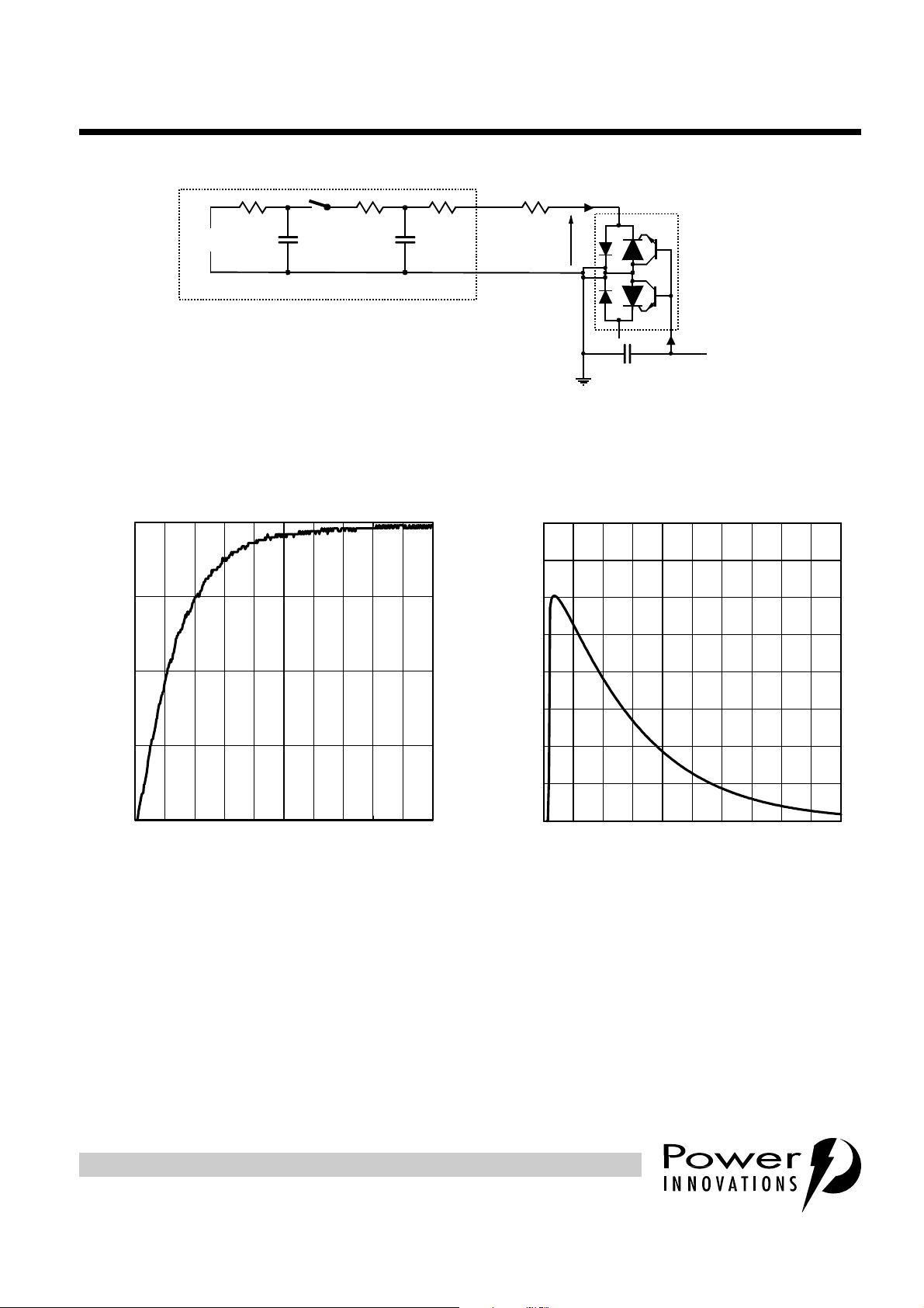
ECAT WITH E502 0.5/700 SURGE NETWORK
R1 = ONE SECTION OF A PBR 530 01/1 LPC LINE
RESISTOR NETWORK
Figure 3. TEST CIRCUIT FOR MEASUREMENT OF LIMITING VOLTAGE
E502 0.5/700 WAVEFRONT CURRENT
vs
TIME
20
15
10
15
25
ΩΩΩΩ
20 nF20 µF
AI6XAY
ΩΩΩΩ
VOLTAGE
Lo
LIMITING
, V
V
K
F
220 nF
Th4
Th5
DUT
(TISPPBL2S)
V
I
GG
G
-50 V
(V
)
BAT
AI6XBAS
i - Wavefront Current - A
5
0
0.0 0.2 0.4 0.6 0.8 1.0 1.2 1.4 1.6 1.8 2.0
Time - µs
Figure 4. CURRENT WAVEFRONT Figure 5. CURRENT WAVEFRONT di/dt
PRODUCT INFORMATION
5
 Loading...