Power Innovations TISPL758LF3D, TISPL758LF3 DR Datasheet

TISPL758LF3D
INTEGRATED SYMMETRICAL AND ASYMMETRICAL BIDIRECTIONAL OVERVOLTAGE
PROTECTORS FOR LUCENT TECHNOLOGIES L7581/2/3 LINE CARD ACCESS SWITCHES
PRODUCT INFORMATION
1
JANUARY 1998 - REVISED OCTOBER 1998Copyright © 1998, Power Innovations Limited, UK
Information is current as of publication date. Products conform to specifications in accordance
with the terms of Power Innovations standard warranty. Production processing does not
necessarily include testing of all parameters.
OVERVOLTAGE PROTECTION FOR LUCENT TECHNOLOGIES LCAS
● Symmetrical and Asymmetrical
Characteristics for Optimum Protection of
Lucent L7581/2/3 LCAS
● Rated for International Surge Wave Shapes
● Ion-Implanted Breakdown Region
Precise And Stable Voltage
Low Voltage Overshoot Under Surge
● Planar Passivated Junctions
Low Off-State Current<±10 µA
● Small Outline Surface Mount Package
- Available Ordering Options
description
The TISPL758LF3 is an integrated combination
of a symmetrical bidirectional overvoltage
protector and an asymmetrical bidirectional
overvoltage protector. It is designed to limit the
peak voltages on the line terminals of the Lucent
Technologies L7581/2/3 LCAS (Line Card
Access Switches). An LCAS may also be
referred to as a Solid State Relay, SSR, i.e. a
replacement of the conventional electromechanical relay.
The TISPL758LF3D voltages are chosen to give
adequate LCAS protection for all switch
conditions. The most potentially stressful
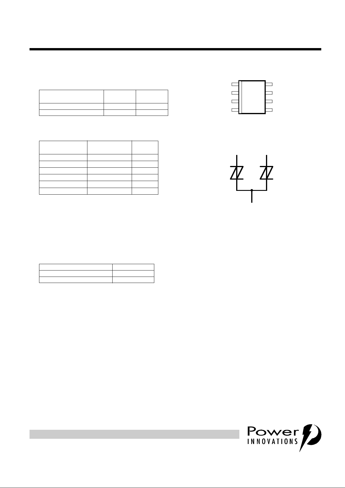
TERMINAL
PAIR
V
DRM
V
V
(BO)
V
T-G (SYMMETRICAL) ±105 ±130
R-G (ASYMMETRICAL) +105, -180 +130, -220
CUSTOMISED VERSIONS AVAILABLE
WAVE SHAPE STANDARD
I
TSP
A
2/10 µs GR-1089-CORE 175
8/20 µs ANSI C62.41 120
10/160 µs FCC Part 68 60
10/700 µs ITU-T K20/21 50
10/560 µs FCC Part 68 45
10/1000 µs GR-1089-CORE 35
CARRIER ORDER #
Tube TISPL758LF3D
Taped and reeled TISPL758LF3DR
condition is low level power cross when the
LCAS switches are closed. Under this condition,
the TISPL758LF3D limits the voltage and
corresponding LCAS dissipation until the LCAS
thermal trip operates and opens the switches.
Under open-circuit ringing conditions, the line
ring (R) conductor will have high peak voltages.
For battery backed ringing, the ring conductor
will have a larger peak negative voltage than
positive i.e. the peak voltages are asymmetric.
An overvoltage protector with a similar voltage
asymmetry will give the most effective protection.
On a connected line, the tip (T) conductor will
have much smaller voltage levels than the opencircuit ring conductor values. Here a symmetrical
voltage protector gives adequate protection.
Overvoltages are normally caused by a.c. power
system or lightning flash disturbances which are
induced or conducted on to the telephone line.
These overvoltages are initially clipped by
protector breakdown clamping until the voltage
rises to the breakover level, which causes the
device symbol
MDXXAE
D PACKAGE
(TOP VIEW)
1
2
3
4 5
6
7
8 G
G
G
G
NC
T
R
NC
NC - No internal connection
G
T R
SD3XAA
Terminals T, R and G correspond to the
alternative line designators of A, B and C
Support from the Microelectronics Group of Lucent Technologies Inc. is gratefully acknowledged in the definition of
the TISPL758LF3D voltage levels and for performing TISPL758LF3D evaluations.

TISPL758LF3D
INTEGRATED SYMMETRICAL AND ASYMMETRICAL BIDIRECTIONAL OVERVOLTAGE
PROTECTORS FOR LUCENT TECHNOLOGIES L7581/2/3 LINE CARD ACCESS SWITCHES
2
JANUARY 1998 - REVISED OCTOBER 1998
PRODUCT INFORMATION
device to crowbar into a low-voltage on state. This low-voltage on state causes the current resulting from the
overvoltage to be safely diverted through the device. For negative surges, the high crowbar holding current
prevents d.c. latchup with the SLIC current, as the surge current subsides. The TISPL758LF3 is guaranteed
to voltage limit and withstand the listed international lightning surges in both polarities.
These protection devices are supplied in a small-outline surface mount (D) plastic package. The difference
between the TISPL758LF3D and TISPL758LF3DR versions is shown in the ordering information.
absolute maximum ratings, T
A
= 25°C (unless otherwise noted)
RATING SYMBOL VALUE UNIT
Repetitive peak off-state voltage R-G terminals
T-G terminals
V
DRM
-180, +105
-105, +105
V
Non-repetitive peak on-state pulse current(see Notes 1, 2 and 3)
I
TSP
A
2/10 µs(GR-1089-CORE, 2/10 µs voltage wave shape) 175
8/20 µs(ANSI C62.41, 1.2/50 µs voltage wave shape) 120
10/160 µs(FCC Part 68, 10/160 µs voltage wave shape) 60
5/200 µs(VDE 0433, 2.0 kV, 10/700 µs voltage wave shape) 50
0.2/310 µs(I3124, 2.0 kV, 0.5/700 µs voltage wave shape) 50
5/310 µs(ITU-T K20/21, 2.0 kV, 10/700 µs voltage wave shape) 50
5/310 µs(FTZ R12, 2.0 kV, 10/700 µs voltage wave shape) 50
10/560 µs(FCC Part 68, 10/560 µs voltage wave shape) 45
10/1000 µs(GR-1089-CORE, 10/1000 µs voltage wave shape) 35
Non-repetitive peak on-state current(see Notes 1, 2 and 3)
I
TSM
16
20
A
full sine wave 50 Hz
60 Hz
Repetitive peak on-state current, 50/60 Hz, (see Notes 2 and 3) I
TSM
2x1 A
Initial rate of rise of on-state current,Exponential current ramp, Maximum ramp value < 70 A di
T
/dt 150 A/µs
Junction temperature T
J
-40 to +150 °C
Storage temperature range T
stg
-40 to +150 °C
NOTES: 1. Above the maximum specified temperature, derate linearly to zero at 150°C lead temperature.
2. Initially the TISPL758LF3 must be in thermal equilibrium with 0°C < T
J
<70°C.
3. The surge may be repeated after the TISPL758LF3 returns to its initial conditions.
recommended operating conditions
MIN TYP MAX UNIT
R1 Series Resistor for GR-1089-CORE first-level surge, operational pass (4.5.7) 20
Ω
R1
Series Resistor for FCC Part 68 10/160 non-operational pass
10/160 operational pass
10/560 non-operational pass
10/560 operational pass
0
18
0
10
Ω
R1
Series Resistor for ITU-T K20/21 10/700, < 2 kV, operational pass
10/700, 4 kV, operational pass
0
40
Ω

3
JANUARY 1998 - REVISED OCTOBER 1998
TISPL758LF3D
INTEGRATED SYMMETRICAL AND ASYMMETRICAL BIDIRECTIONAL OVERVOLTAGE
PROTECTORS FOR LUCENT TECHNOLOGIES L7581/2/3 LINE CARD ACCESS SWITCHES
PRODUCT INFORMATION
NOTES: 4. Positive and negative values of V
DRM
are not equal. See ratings table
5. These capacitance measurements employ a three terminal capacitance bridge incorporating a guard circuit. The third terminal is
connected to the guard terminal of the bridge.
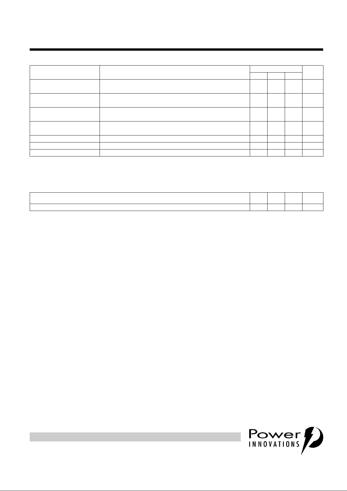
electrical characteristics for the T-G and R-G terminal pairs, TJ = 25°C (unless otherwise noted)
PARAMETER TEST CONDITIONS
VALUE
UNIT
MIN TYP MAX
I
DRM
Repetitive peak offstate current
V
D
= ±V
DRM
, (See Note 4) ±10 µA
V
(BO)
Breakover voltage dv/dt = ±250 V/ms,R
SOURCE
= 300 Ω
R-G terminals
T-G terminals
-220
-130
+130
+130
V
V
(BO)
Impulse breakover voltage
Rated impulse conditions with operational pass series
resistor
R-G terminals
T-G terminals
-240
-140
+140
+140
V
I
H
Holding current
di/dt = -30 mA/ms
di/dt = +30 mA/ms
+100
-150
mA
I
D
Off-state current 0 < VD < ±50 V, TJ = 85°C ±10 µA
C
TG
Off-state capacitance f = 100 kHz,Vd= 1 V rms VTG= -5 V, (See Note 5) 18 36 pF
C
RG
Off-state capacitance f = 100 kHz,Vd= 1 V rms VTG= -50 V, (See Note 5) 10 20 pF
thermal characteristics
PARAMETER
MIN TYP MAX
UNIT
R
θJA
Junction to free air thermal resistance 160 °C/W
 Loading...