Power Innovations TISP7082F3SL, TISP7082F3P, TISP7082F3DR, TISP7082F3D, TISP7072F3SL Datasheet
...
TISP7072F3, TISP7082F3
TRIPLE BIDIRECTIONAL THYRISTOR OVERVOLTAGE PROTECTORS
MARCH 1994 - REVISED MARCH 2000Copyright © 2000, Power Innovations Limited, UK
TELECOMMUNICATION SYSTEM SECONDARY PROTECTION
● Patented Ion-Implanted Breakdown Region
– Precise DC and Dynamic Voltages
V
DEVICE
‘7072F3 58 72
‘7082F3 66 82
DRM
V
● Planar Passivated Junctions
V
(BO)
V
– Low Off-State Current....................< 10 µA
● Rated for International Surge Wave Shapes
– Single and Simultaneous Impulses
I
WAVE SHAPE STANDARD
2/10 GR-1089-CORE 85
8/20 IEC 61000-4-5 80
10/160 FCC Part 68 65
10/700
10/560 FCC Part 68 45
10/1000 GR-1089-CORE 40
FCC Part 68
ITU-T K.20/21
TSP
A
50
● ..................UL Recognized Component
description
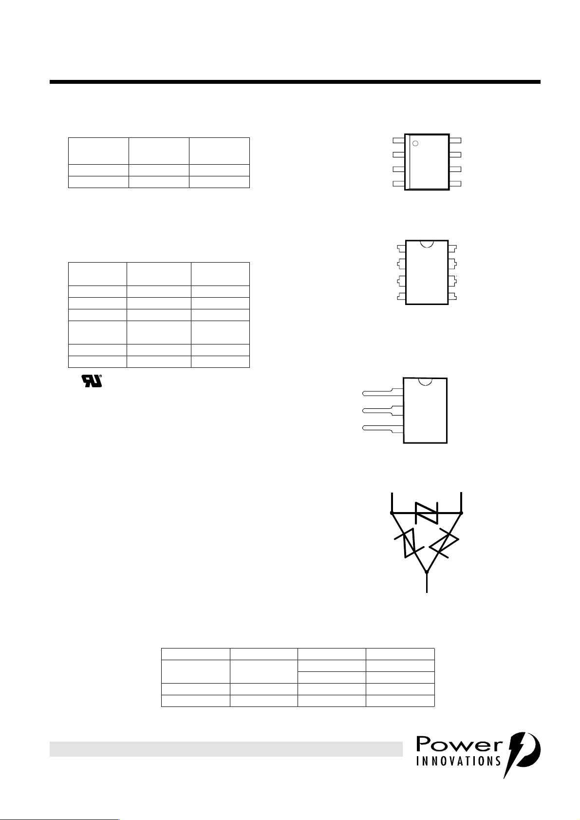
The TISP7xxxF3 series are 3-point overvoltage
protectors designed for protecting against
metallic (differential mode) and simultaneous
longitudinal (common mode) surges. Each
terminal pair has the same voltage limiting
values and surge current capability. This terminal
pair surge capability ensures that the protector
can meet the simultaneous longitudinal surge
requirement which is typically twice the metallic
surge requirement.
NC - No internal connection
NU - Nonusable; no external electrical connection
should be made to these pins.
Specified ratings require connection of pin 5 and
pin 8.
T
G
R
device symbol
T
NC
NC
R
T
NC
NC
R
T
D PACKAGE
(TOP VIEW)
1
2
3
45
P PACKAGE
(TOP VIEW)
1
2
3
4
SL PACKAGE
(TOP VIEW)
1
2
3
8
7
6
8
7
6
5
G
NU
NU
G
G
NU
NU
G
R
MDXXAL
MDXXAJ A
MDXXAGA
MD7XAACA
Each terminal pair has a symmetrical voltagetriggered thyristor characteristic. Overvoltages
are initially clipped by breakdown clamping until
the voltage rises to the breakover level, which
causesthedevicetocrowbarintoalow-voltage
on state. This low-voltage on state causes the
current resulting from the overvoltage to be .
AVAILABLE OPTIONS
DEVICE PACKAGE CARRIER ORDER #
TISP7xxxF3 D, Small-outline
TISP7xxxF3 P, Plastic DIP TUBE TISP7xxxF3P
TISP7xxxF3 SL, Single-in-line TUBE TISP7xxxF3SL
TAPE AND REEL TISP7xxxF3DR
TUBE TISP7xxxF3D
PRODUCT INFORMATION
Information is current as of publication date. Products conform to specifications in accordance
with the terms of Power Innovations standard warranty. Production processing does not
necessarily include testing of all parameters.
SD7XAB
G
TerminalsT,RandGcorrespondtothe
alternative line designators of A, B and C
1

TISP7072F3, TISP7082F3
TRIPLE BIDIRECTIONAL THYRISTOR OVERVOLTAGE PROTECTORS
MARCH 1994 - REVISED MARCH 2000
description (continued)
safely diverted through the device. The high crowbar holding current prevents d.c. latchup as the diverted
current subsides.These protectors are guaranteed to voltage limit and withstand the listed lightning surges in
both polarities.
These low voltage devices are guaranteed to suppress and withstand the listed international lightning surges
on any terminal pair. Nine similar devices with working voltages from 100 V to 275 V are detailed in the
TISP7125F3 thru TISP7380F3 data sheet.
absolute maximum ratings, TA= 25 °C (unless otherwise noted)
RATING SYMBOL VALUE UNIT
Repetitive peak off-state voltage, 0 °C < T
Non-repetitive peak on-state pulse current (see Notes 1 and 2)
1/2 (Gas tube differential transient, 1/2 voltage wave shape) 240
2/10 (Telcordia GR-1089-CORE, 2/10 voltage wave shape) 85
1/20 (ITU-T K.22, 1.2/50 voltage wave shape, 25 Ω resistor) 45
8/20 (IEC 61000-4-5, combination wave generator, 1.2/50 voltage wave shape) 80
10/160 (FCC Part 68, 10/160 voltage wave shape) 65
4/250 (ITU-T K.20/21, 10/700 voltage wave shape, simultaneous) 60
0.2/310 (CNET I 31-24, 0.5/700 voltage wave shape) 50
5/310 (ITU-T K.20/21, 10/700 voltage wave shape, single) 50
5/320 (FCC Part 68, 9/720 voltage wave shape, single) 50
10/560 (FCC Part 68, 10/560 voltage wave shape) 45
10/1000 (Telcordia GR-1089-CORE, 10/1000 voltage wave shape) 40
Non-repetitive peak on-state current, 0 °C < T
50 Hz, 1 s D Package
Initial rate of rise of on-state current, Linear current ramp, Maximum ramp value < 38 A di
Junction temperature T
Storage temperature range T
<70°C
A
<70°C (seeNotes1and3)
A
‘7072F3
‘7082F3
PPackage
SL Package
V
DRM
I
PPSM
I
TSM
/dt 250 A/µs
T
J
stg
58
66
4.3
5.7
7.1
-65to+150 °C
-65to+150 °C
V
A
A
NOTES: 1. Initially the TISP
initial conditions. The rated current values may be applied singly either to the R to G or to the T to G or to the T to R terminals.
Additionally, both R to G and T to G may have their rated current values applied simultaneously (In this case the total G terminal
current will be twice the above rated current values).
2. See Thermal Information for derated I
3. Above 70 °C, derate I
®
must be in thermal equilibrium at the specified TA. The surge may be repeated after the TISP®returns to its
values 0 °C < TA< 70 °C and Applications Information for details on wave shapes.
linearly to zero at 150 °C lead temperature.
TSM
PPSM
PRODUCT INFORMATION
2

TISP7072F3, TISP7082F3
TRIPLE BIDIRECTIONAL THYRISTOR OVERVOLTAGE PROTECTORS
MARCH 1994 - REVISED MARCH 2000
electrical characteristics for all terminal pairs, TA= 25 °C (unless otherwise noted)
PARAMETER TEST CONDITIONS MIN TYP MAX UNIT
I
DRM
V
(BO)
V
(BO)
I
(BO)
V
T
I
H
dv/dt
I
D
C
off
Repetitive peak offstate current
Breakover voltage dv/dt = ±250 V/ms, R
Impulse breakover
voltage
Breakover current dv/dt = ±250 V/ms, R
On-state voltage IT=±5A,tW=100µs ±5 V
Holding current IT= ±5 A, di/dt = +/-30 mA/ms ±0.15 A
Critical rate of rise of
off-state voltage
Off-state current VD=±50V ±10 µA
Off-state capacitance
V
D=VDRM
,0°C<TA< 70 °C ±10 µA
=300Ω
SOURCE
dv/dt ≤ ±1000 V/µs, Linear voltage ramp,
Maximum ramp value = ±500 V
di/dt = ±20 A/µs, Linear current ramp,
Maximum ramp value = ±10 A
=300Ω ±0.1 ±0.8 A
SOURCE
Linear voltage ramp, Maximum ramp value < 0.85V
f=1MHz, V
f=1MHz, V
f=1MHz, V
f=1MHz, V
f=1MHz, V
=1Vrms,VD=0
d
=1Vrms,VD=-1V
d
=1Vrms,VD=-2V
d
=1Vrms,VD=-5V
d
=1Vrms,VD=-50V
d
DRM
‘7072F3
‘7082F3
‘7072F3
‘7082F3
±5 kV/µs
53
56
51
43
25
±72
±82
±90
±100
69
73
66
56
33
V
V
pF
37
f=1MHz, V
=1Vrms,V
d
DTR
=0
29
(see Note 4)
NOTE 4: Three-terminal guarded measurement, unmeasured terminal voltage bias is zero. First five capacitance values, with bias V
for the R-G and T-G terminals only. The last capacitance value, with bias V
, is for the T-R terminals.
DTR
,are
D
PRODUCT INFORMATION
3
TISP7072F3, TISP7082F3
TRIPLE BIDIRECTIONAL THYRISTOR OVERVOLTAGE PROTECTORS
MARCH 1994 - REVISED MARCH 2000
thermal characteristics
PARAMETER
P
R
Junction to free air thermal resistance
θJA
tot
5cm
TEST CONDITIONS
=0.8W, TA=25°C
2
,FR4PCB
D Package 160
SL Package 135
MIN TYP MAX UNIT
°C/WP Package 100
PARAMETER MEASUREMENT INFORMATION
+i
I
TSP
Characteristic
Quadrant I
Switching
-v
I
(BO)
V
Quadrant III
Switching
Characteristic
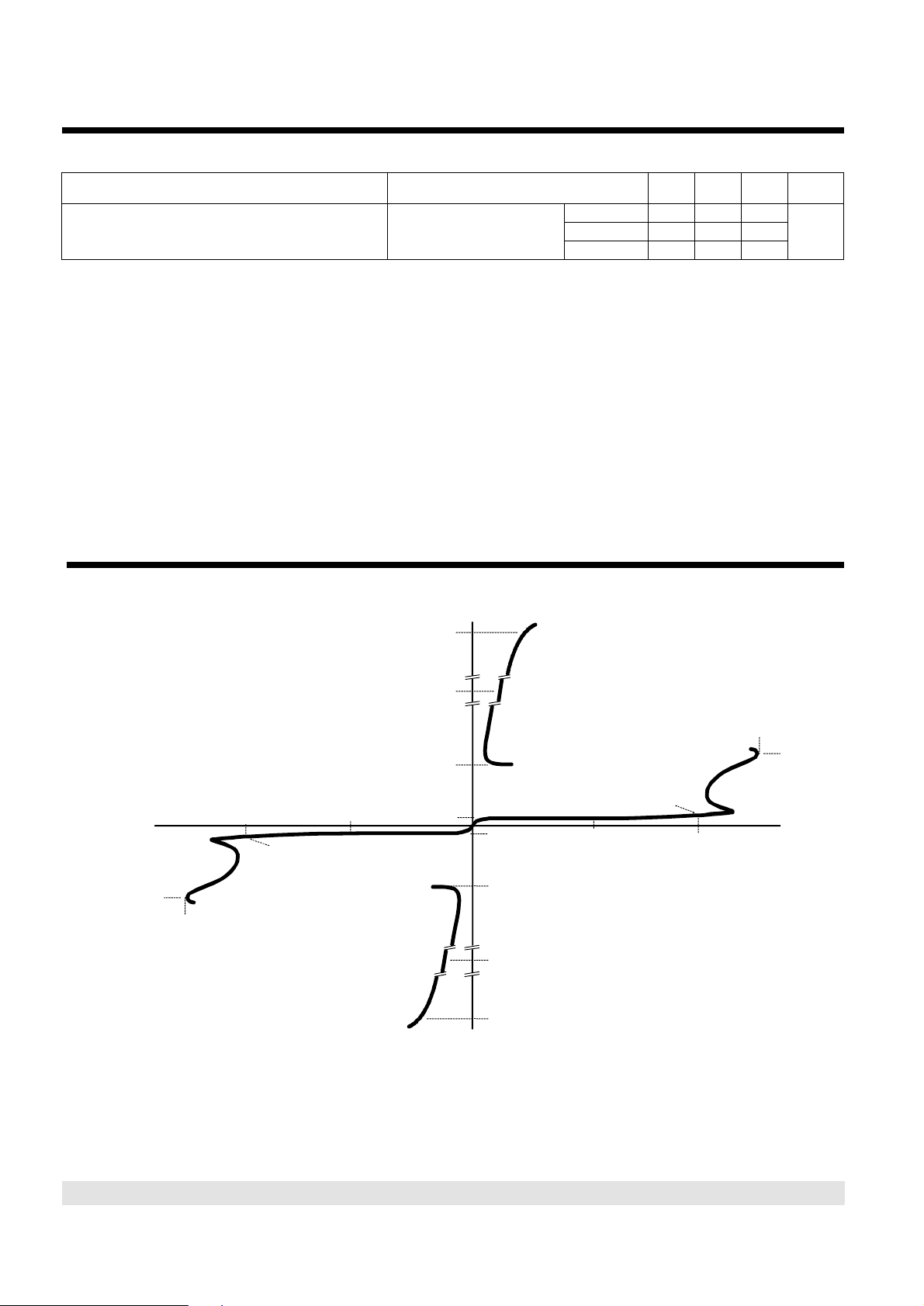
Figure 1. VOLTAGE-CURRENT CHARACTERISTIC FOR T AND R TERMINALS
(BO)
I
TSM
I
H
I
V
DRM
I
DRM
V
D
I
D
I
D
I
H
I
TSM
I
TSP
V
D
DRM
V
DRM
-i
T and G and R and G measurements are referenced to the G terminal
T and R measurements are referenced to the R terminal
V
(BO)
PMXXAAA
I
(BO)
+v
PRODUCT INFORMATION
4
TISP7072F3, TISP7082F3
TRIPLE BIDIRECTIONAL THYRISTOR OVERVOLTAGE PROTECTORS
MARCH 1994 - REVISED MARCH 2000
TYPICAL CHARACTERISTICS
R and G, or T and G terminals
- Off-State Current - µA
D
I
100
10
0·1
0·01
0·001
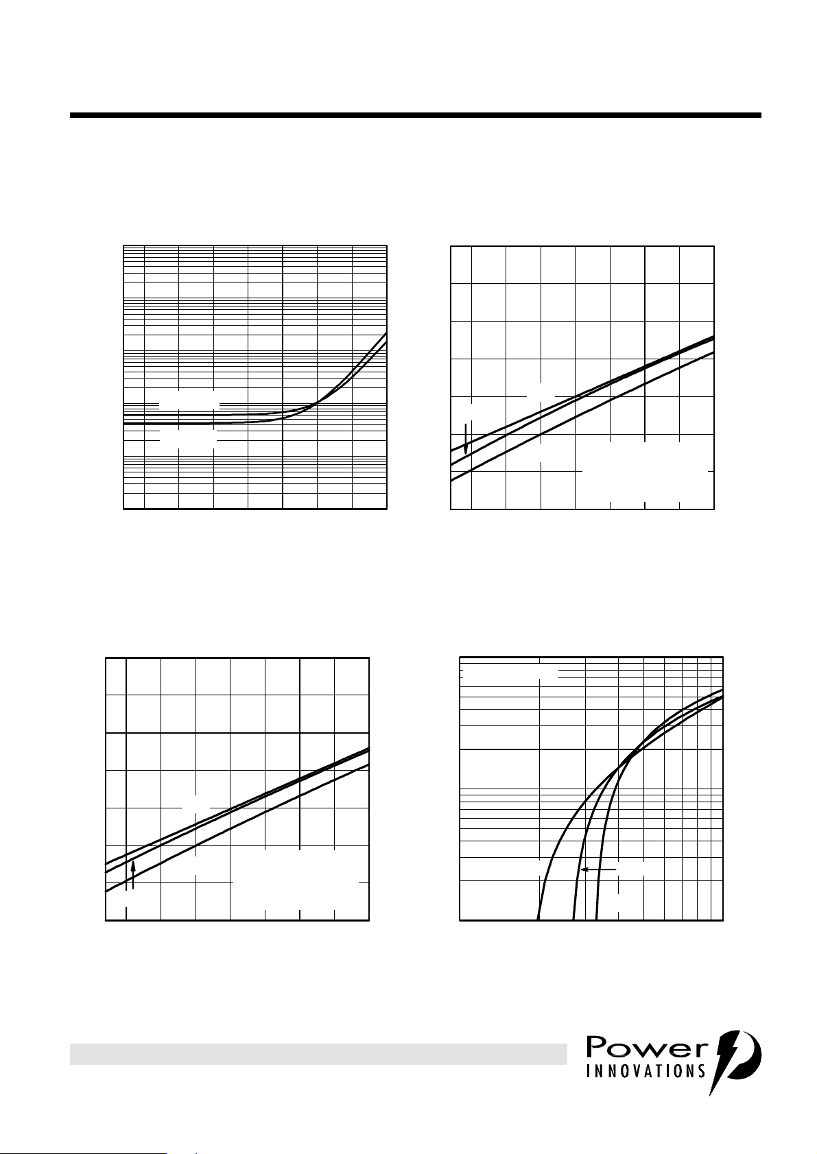
OFF-STATE CURRENT
vs
JUNCTION TEMPERATURE
1
VD=-50V
VD=50V
-25 0 25 50 75 100 125 150
TJ- Junction Temperature - °C
Figure 2. Figure 3.
TC7LAC
NORMALISED BREAKDOWN VOLTAGES
vs
JUNCTION TEMPERATURE
1.2
1.1
V
(BO)
V
(BR)M
1.0
Normalised Breakdown Voltages
0.9
-25 0 25 50 75 100 125 150
V
(BR)
TJ- Junction Temperature - °C
Normalised to V
I
=1mAand25°C
(BR)
Positive Polarity
TC7LAE
(BR)
NORMALISED BREAKDOWN VOLTAGES
vs
JUNCTION TEMPERATURE
1.2
1.1
V
(BO)
1.0
Normalised Breakdown Voltages
V
(BR)M
0.9
-25 0 25 50 75 100 125 150
V
(BR)
TJ- Junction Temperature - °C
Normalised to V
I
=1mAand25°C
(BR)
Negative Polarity
Figure 4. Figure 5.
TC7LAF
(BR)
ON-STATE CURRENT
vs
ON-STATE VOLTAGE
100
Positive Polarity
10
- On-State Current - A
T
I
150°C
1
23456789110
VT- On-State Voltage - V
25°C
-40°C
TC7LAL
PRODUCT INFORMATION
5
TISP7072F3, TISP7082F3
TRIPLE BIDIRECTIONAL THYRISTOR OVERVOLTAGE PROTECTORS
MARCH 1994 - REVISED MARCH 2000
TYPICAL CHARACTERISTICS
R and G, or T and G terminals
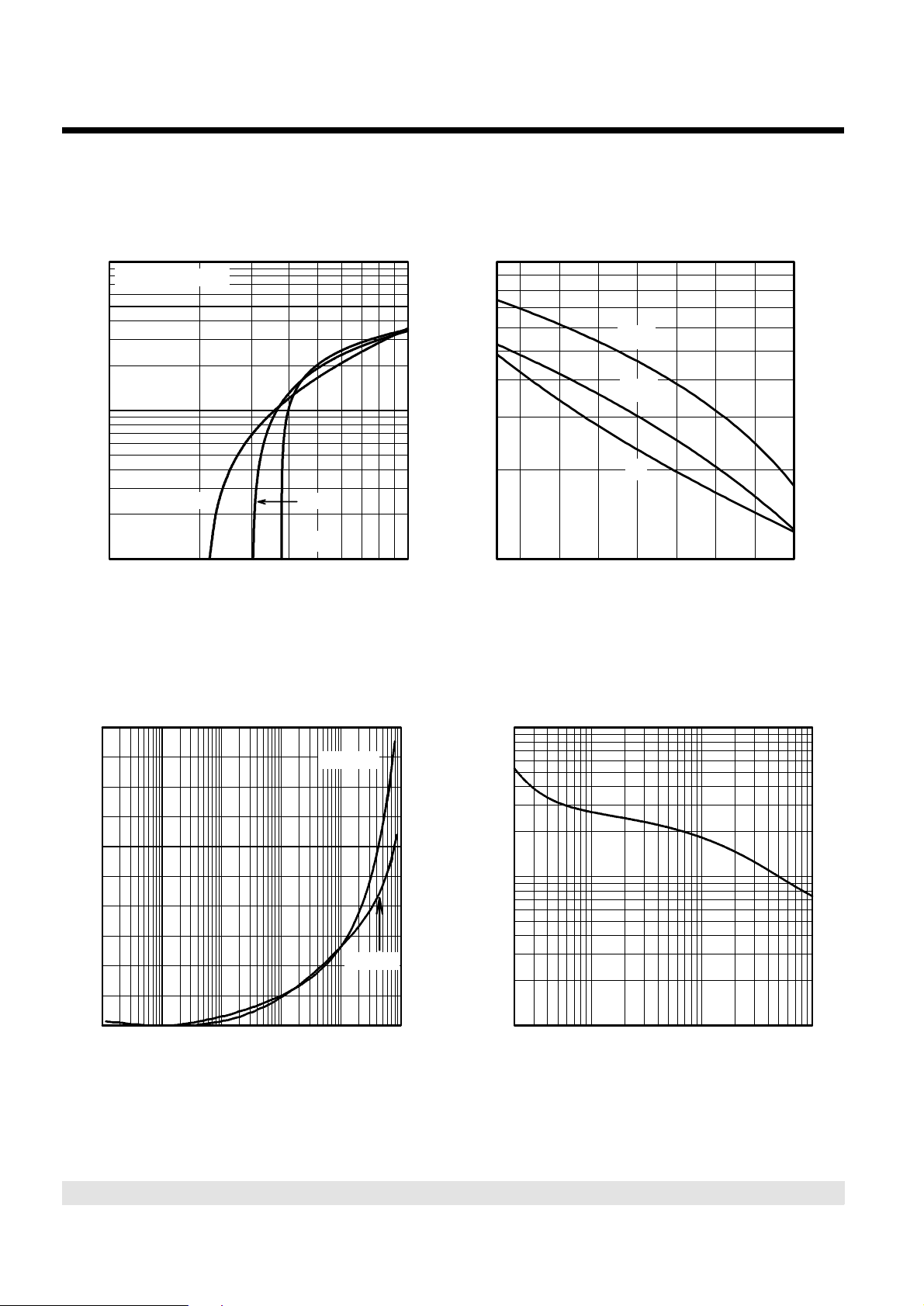
ON-STATE CURRENT
vs
ON-STATE VOLTAGE
100
Negative Polarity
10
- On-State Current - A
T
I
150°C
1
23456789110
VT- On-State Voltage - V
25°C
-40°C
TC7LAM
HOLDING CURRENT & BREAKOVER CURRENT
vs
- Holding Current, Breakover Current - A
,I
I
JUNCTION TEMPERATURE
1.0
0.9
0.8
0.7
0.6
0.5
0.4
0.3
0.2
(BO)
H
0.1
-25 0 25 50 75 100 125 150
TJ- Junction Temperature - °C
+I
(BO)
-I
(BO)
I
H
TC7LAH
Figure 6. Figure 7.
NORMALISED BREAKOVER VOLTAGE
vs
RATE OF RISE OF PRINCIPLE CURRENT
1.5
1.4
1.3
1.2
Normalised Breakover Voltage
1.1
1.0
0·001 0·01 0·1 1 10 100
di/dt - Rate of Rise of Principle Current - A/µs
TC7LAU
Negative
Positive
Figure 8. Figure 9.
1000
Maximum Surge Current - A
100
10
SURGE CURRENT
vs
DECAY TIME
2
10 100 1000
Decay Time - µs
TC7LAA
PRODUCT INFORMATION
6
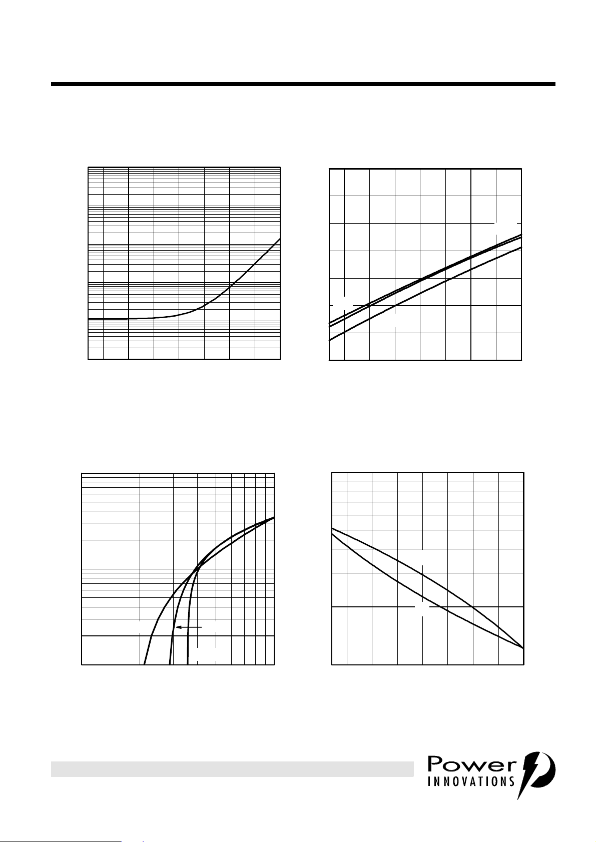
TISP7072F3, TISP7082F3
TRIPLE BIDIRECTIONAL THYRISTOR OVERVOLTAGE PROTECTORS
MARCH 1994 - REVISED MARCH 2000
TYPICAL CHARACTERISTICS
RandTterminals
- Off-State Current - µA
D
I
100
10
0·1
0·01
0·001
OFF-STATE CURRENT
vs
JUNCTION TEMPERATURE
1
-25 0 25 50 75 100 125 150
TJ- Junction Temperature - °C
Figure 10. Figure 11.
TC7LAD
NORMALISED BREAKDOWN VOLTAGES
vs
JUNCTION TEMPERATURE
1.2
1.1
V
(BO)
1.0
Normalised Breakdown Voltages
0.9
-25 0 25 50 75 100 125 150
V
(BR)
TJ- Junction Temperature - °C
TC7LAG
V
(BR)M
ON-STATE CURRENT
vs
ON-STATE VOLTAGE
100
10
- On-State Current - A
T
I
150°C
1
23456789110
VT- On-State Voltage - V
25°C
-40°C
TC7LAK
HOLDING CURRENT & BREAKOVER CURRENT
vs
- Holding Current, Breakover Current - A
,I
I
JUNCTION TEMPERATURE
1.0
0.9
0.8
0.7
0.6
0.5
0.4
0.3
0.2
(BO)
H
0.1
-25 0 25 50 75 100 125 150
TJ- Junction Temperature - °C
I
(BO)
I
H
TC7LAJ
Figure 12. Figure 13.
PRODUCT INFORMATION
7
 Loading...