Power Innovations TISP61089P, TISP61089DR, TISP61089D Datasheet

PROGRAMMABLE SLIC OVERVOLTAGE PROTECTION FOR LSSGR ‘1089
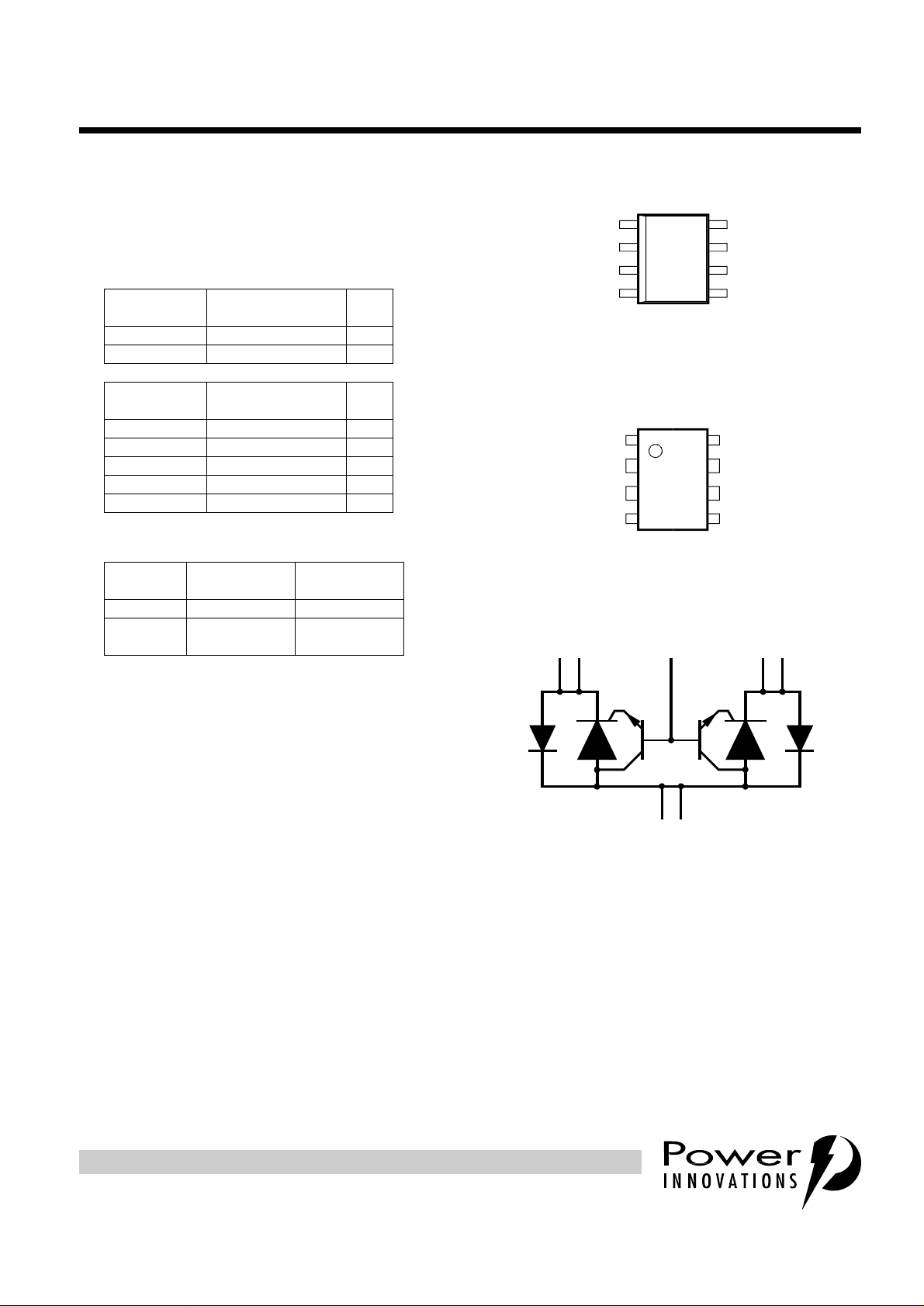
device symbol
Terminals K1, K2 and A correspond to the alternative
line designators of T, R and G or A, B and C. The
negative protection voltage is controlled by the voltage,
V
GG,
applied to the G
terminal.
SD6XAE
AK1G
K2
y
(
)
(
)
(
)
(
g)
(
)
(
)
(
g)
y
(
)
(
)
(
)
(
g)
(
)
(
)
(
g)
●
Dual Voltage-Programmable Protectors
- Wide 0 to -85 V Programming Range
- Low 5 mA max. Gate Triggering Current
- High 150 mA min. Holding Current
●
Rated for LSSGR ‘1089 Conditions
WAVE SHAPE
2/10 µs 4.5.8 Second-Level 1 120
10/1000 µs 4.5.7 First-Level 3 30
‘1089 TEST CLAUSE
AND TEST #
TISP61089
DUAL FORWARD-CONDUCTING P-GATE THYRISTORS
PROGRAMMABLE OVERVOLTAGE PROTECTORS
NOVEMBER 1995 - REVISED FEBRUARY 1998Copyright © 1998, Power Innovations Limited, UK
D PACKAGE
(TOP VIEW)
I
TSP
K1
Tip
G
Gate
NC
K2
Rin
A
Terminal t
NC - No internal connection
1
2
3
45
pical application names shown in
parenthesis
8
K1
Tip
7
6
A
A
K2
Ground
Ground
Rin
MD6XAN
60 Hz POWER
FAULT TIME
100 ms 4.5.13 Second-Level 2 11
1 s 4.5.13 Second-Level 2 4.5
5 s 4.5.13 Second-Level 2 2.4
300 s 4.5.13 Second-Level 1 0.95
900 s 4.5.13 Second-Level 1 0.93
●
2/10 Protection Voltage Specified
ELEMENT
Diode 6 8
Crowbar
= -48 V
V
GG
●
Also Rated for ITU-T 10/700 impulses
●
Surface Mount and Through-Hole Options
‘1089 TEST CLAUSE
AND TEST #
FIRST-LEVEL
V @ 56 A
-57 -60
I
TSM
A
SECOND-LEVEL
V @ 100 A
P PACKAGE
(TOP VIEW)
Tip
Gate
Rin
Terminal t
1
K1
2
G
3
NC
45
K2
NC - No internal connection
pical application names shown in
parenthesis
8
7
6
K1
A
A
K2
Tip
Ground
Ground
Rin
MD6XAV
- TISP61089P for Plastic DIP
- TISP61089D for Small-Outline
- TISP61089DR for Small-Outline Taped and
Reeled
description
The TISP61089 is a dual forward-conducting
buffered p-gate overvoltage protector. It is
designed to protect monolithic SLICs (Subscriber
Line Interface Circuits) against overvoltages on
the telephone line caused by lightning, a.c.
power contact and induction. Th e TISP61089 limits voltages that exceed the SLIC supp ly rail voltage. The
TISP61089 parameters are specified to allow equipment compliance with Bellcore GR-1089-CORE, Issue 1.
The SLIC line driver section is typically powered from 0 V (ground) and a negative voltage in the region of
-10 V to -75 V. The protector gate is connected to this negative supply. This references the protection
(clipping) voltage to the ne gative supply voltage. As the pro tectio n voltage wil l then track the nega tive supply
voltage the overvoltage stress on the SLIC is minimised.
Positive overvoltages are cl ipped to ground by diode forward condu ction. Negative overvoltages are i nitially
clipped close to the SLIC negative supply rail value. If sufficient current is available from the overvoltage, then
PRODUCT INFORMATION
Information is current as of publication date. Products conform to specifications in accordance
with the terms of Power Innovations standard warranty. Production processing does not
necessarily include testing of all parameters.
1

TISP61089
DUAL FORWARD-CONDUCTING P-GATE THYRISTORS
PROGRAMMABLE OVERVOLTAGE PROTECTORS
NOVEMBER 1995 - REVISED FEBRUARY 1998
the protector will c rowbar int o a low voltage on-s tate cond ition. As the overvoltage subs ides the high holdi ng
current of the crowbar prevents d.c. latchup.
The TISP61089 is intended to be used with a series combination of a 25Ω or higher resistance and a suitable
overcurrent protector. Power fault compliance requires the series overcurrent element to open-circuit or
become high impedance (see Applications Information). For equipment compliant to ITU-T recommendations
K20 or K21 only, the series resistor value is set by the power cross requirements. For K20 and K21, a
minimum series resistor value of 10Ω is recommended.
These monolithic protection devices a re fabricated in ion-impla nted planar ver tical power structures for high
reliability and in normal system operation they are virtually transparent. The TISP61089 buffered gate design
reduces the loading on the SLIC supply during overvoltages caused by power cross and induction. The
TISP61089 is available in 8-pin plastic small-outline surface mount package and 8-pin plastic dual-in-line
package.
absolute maximum ratings
RAT ING SYMBOL VALUE UNIT
≤
Repetitive peak off-state voltage, I
Repetitive peak gate-cathode voltage, V
Non-repetitive peak on-state pulse current (see Notes 1 and 2)
10/1000 µs (Bellcore GR-1089-CORE, Issue 1, November 1994, Section 4)
5/320 µs (ITU-T recommendation K20 & K21, open-circuit voltage wave shape 10/700)
1.2/50 µs (Bellcore GR-1089-CORE, Issue 1, November 1994, Section 4, Alternative) 100
2/10 µs (Bellcore GR-1089-CORE, Issue 1, November 1994, Section 4) 120
Non-repetitive peak on-state current, 60 Hz (see Notes 1 and 2)
0.1 s 11
1s
5s
300 s
900 s
Non-repetitive peak gate current, 1/2 µs pulse, cathodes commoned (see Notes 1 and 2) I
Operating free-air temperature range T
Junction temperature T
Storage temperature range T
= 0, -40°C≤T
G
= 0, -40°C≤T
KA
85°C V
J
≤
85°C V
J
DRM
GKRM
I
TSP
I
TSM
GSM
A
J
stg
-100 V
-85 V
30
40
4.5
2.4
0.95
0.93
40 A
-40 to +85 °C
-40 to +150 °C
-40 to +150 °C
A
A
NOTES: 1. Initially the protector must be in thermal equilibrium with -40°C≤T
its initial conditions.
2. The rated current values may be applied either to the Ring to Ground or to the Tip to Ground ter minal pairs. Additionally, both
terminal pairs may have thei r rated current values applied simultaneously (in this case the Ground terminal current will be twice the
rated current value of an individual terminal pair). Above 85°C, derate linearly to zero at 150°C lead temperature.
recommended operating conditions
C
Gate decoupling capacitor 100 220 nF
G
TISP61089 series resistor for first-level and second-level surge survival
R
S
TISP61089 series resistor for first-level surge survival
PRODUCT INFORMATION
2
≤
85°C. The surge may be repeated after the device returns to
J
MIN TYP MAX UNIT
40
25
Ω

DUAL FORWARD-CONDUCTING P-GATE THYRISTORS
PROGRAMMABLE OVERVOLTAGE PROTECTORS
electrical characterist ics, TJ = 25°C (unless otherwise noted)
PARAMETER TEST CONDITIONS MIN TYP MAX UNIT
I
D
V
V
V
I
H
I
GAS
I
GT
V
Q
C
(BO)
F
FRM
GT
GS
AK
Off-state current VD=-85V, VGK=0
Ω,
VGG=-48V, CG= 220 nF
Ω,
VGG=-48V, CG= 220 nF
Ω,
VGG=-48V, CG= 220 nF
Ω,
VGG=-48V, CG= 220 nF
Breakover voltage
2/10 µs, I
2/10 µs, I
1.2/50 µs, I
1.2/50 µs, I
= -56 A, RS=45
T
= -100 A, RS=50
T
=-53A, RS=47
T
=-96A, RS=52
T
Forward voltage IF= 5 A, tw= 200 µs 3V
Ω,
VGG=-48V, CG= 220 nF
Ω,
VGG=-48V, CG= 220 nF
Ω,
VGG=-48V, CG= 220 nF
Ω,
VGG=-48V, CG= 220 nF
Peak forward recov ery
voltage
2/10 µs, I
2/10 µs, I
1.2/50 µs, I
1.2/50 µs, I
=56A, RS=45
F
= 100 A, RS=50
F
=53A, RS=47
F
=96A, RS=52
F
Holding current IT= -1 A, di/dt = 1A/ms, VGG= -48 V -150 mA
Gate reverse current VGG=VGK=-75V, VKA=0
≥
Gate trigger current IT= 3 A, t
Gate trigger voltage IT= 3 A, t
p(g)
p(g)
20 µs, V
≥
20 µs, V
=-48V 5 mA
GG
=-48V 2.5 V
GG
Gate switching charge 1.2/50 µs, IT=53A, RS=47Ω, VGG= -48 V CG= 220 nF 0.1 µC
Anode-cathode off-
state capacitance
f=1MHz, V
=1V, IG= 0, (see Note 3)
d
T
T
T
T
V
V
TISP61089
NOVEMBER 1995 - REVISED FEBRUARY 1998
= 25°C -5 µA
J
= 85°C -50 µA
J
-57
-60
-60
-64
6
8
8
12
= 25°C -5 µA
J
= 85°C -50 µA
J
= -3 V 100 pF
D
=-48V 50 pF
D
V
V
NOTE 3: These capacitance mea surements employ a three terminal capacitance bridge incorporating a guard circuit. The unmeasured
device terminals are a.c. connected to the guard terminal of the bridge.
thermal characteristics
PARAMETER TEST CONDITIONS MIN TYP MAX UNIT
P
=0.8W, TA= 25°C
R
Junction to free air thermal resistance
θ
JA
tot
5cm
2
, FR4 PCB
D Package 160
P Package 100
°C/W
PRODUCT INFORMATION
3

TISP61089
DUAL FORWARD-CONDUCTING P-GATE THYRISTORS
PROGRAMMABLE OVERVOLTAGE PROTECTORS
NOVEMBER 1995 - REVISED FEBRUARY 1998
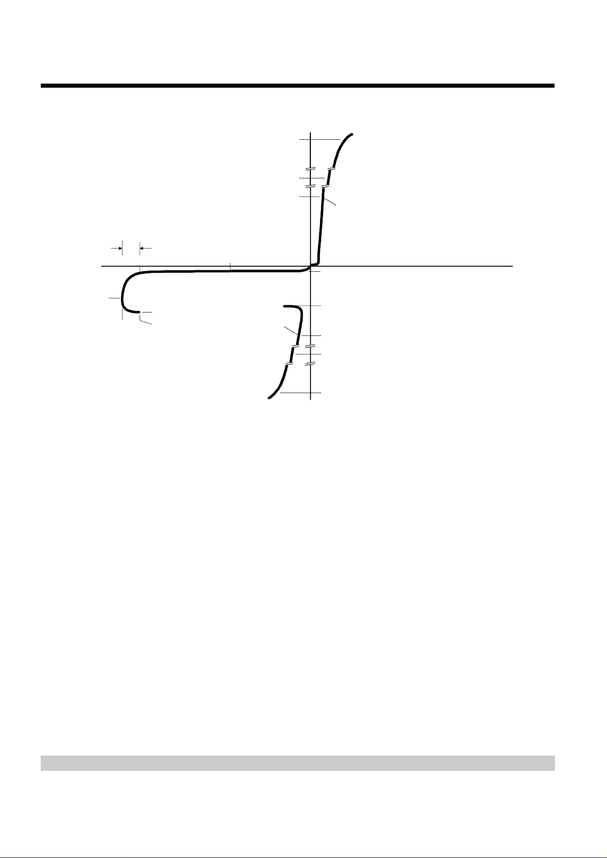
PARAMETER MEASUREMENT INFORMATION
-v
I
(BO)
V
Quadrant III
Switching
Characteristic
V
(BO)
GK(BO)
V
+i
I
(= |I
TSP
|)
FSP
Characteristic
I
(= |I
FSM
GG
I
S
V
S
V
D
|)
TSM
I
F
V
F
I
D
I
H
V
T
I
T
I
TSM
I
TSP
-i
Quadrant I
Forward
Conduction
+v
PM6XAAA
Figure 1. VOLTAGE-CURRENT CHARACTERISTIC
PRODUCT INFORMATION
4

g
10
DUAL FORWARD-CONDUCTING P-GATE THYRISTORS
PROGRAMMABLE OVERVOLTAGE PROTECTORS
NOVEMBER 1995 - REVISED FEBRUARY 1998
THERMAL INFORMATION
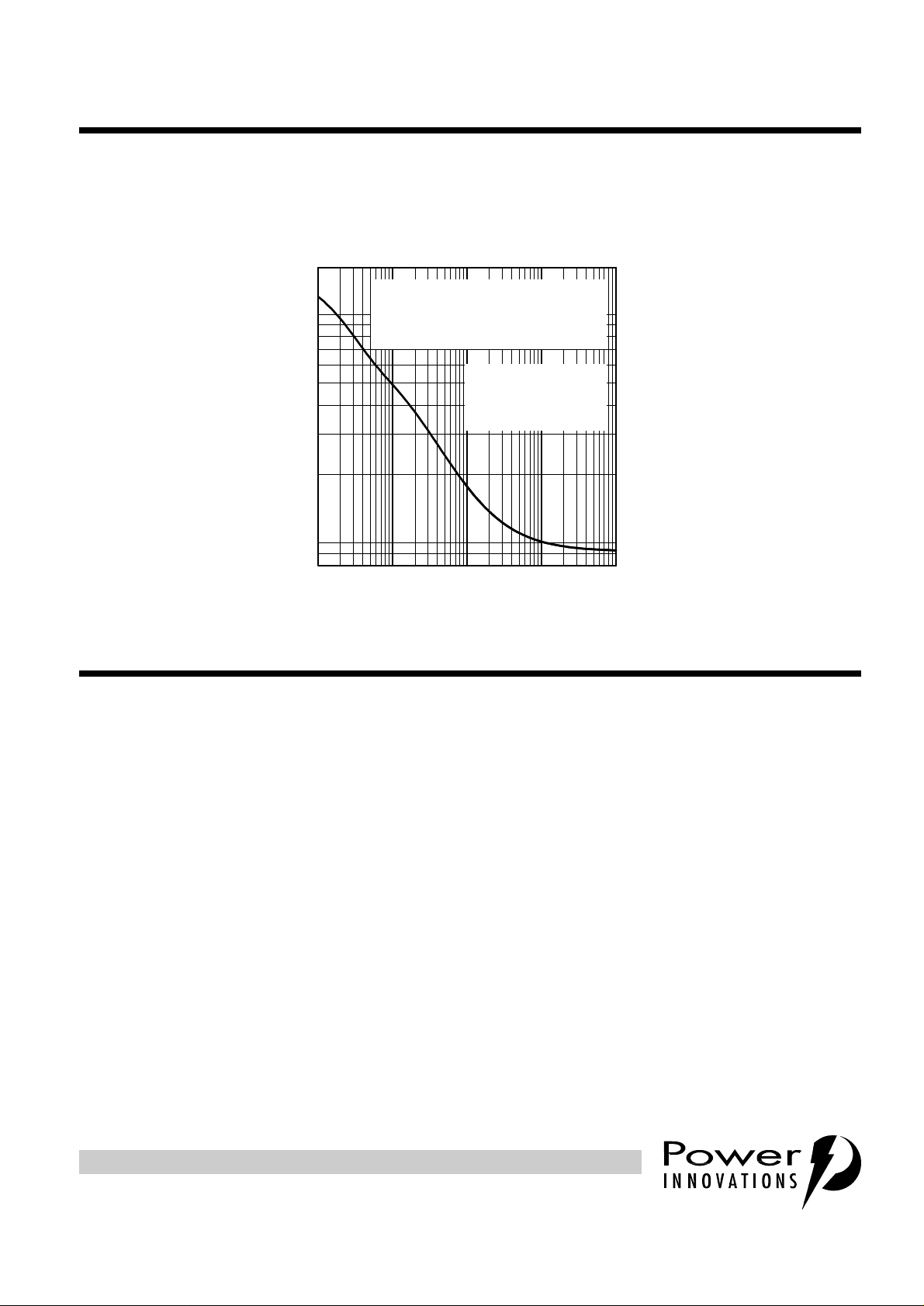
PEAK NON-RECURRING A.C.
vs
CURRENT DURATION
RING AND TIP CONNECTIONS -
applied simultaneously to both
I
TSM
GROUND CONNECTION Return current is twice I
V
GEN
R
GEN
VG = -48 V, T
TSM
= 600 Vrms
= 70 to 950
AMB
TI6LACA
Ω
= 85°C
TISP61089
- Peak Non-Recurrent 60 Hz Current - A
TSM
1
I
0·1 1 10 100 1000
t - Current Duration - s
Fi
ure 2. NON-REPETITIVE PEAK ON-STATE CURRENT AGAINST DURATION
APPLICATIONS INFORMATION
gated protectors
This section covers three topics. Firstly, it is explained why gated protectors are needed. Second, the voltage
limiting action of the protector is described. Third, an example application circuit is described.
purpose of gated protectors
Fixed voltage thyristor overvoltage protectors have been used si nce the early 1980s to protect mo nolithic
SLICs (Subscriber Line Interface Circuits) against overvoltages on the telephone line caused by lightning, a.c.
power contact and induction. As the SLIC was usuall y powered from a fixed voltage negative supply rail, the
limiting voltage of the protector could als o be a fixed value. The TISP1072F3 is a typical example of a fixed
voltage SLIC protector.
SLICs have become more sophisticated. T o minimise power consumption, some designs automatically adjust
the supply voltage, V
supply voltage would be set low, but for long lines, a higher supply voltage would be generated to drive
sufficient line curren t. The optimum protection for this type of SLIC would be given by a protection voltage
which tracks the SLIC supply voltage. This can be achieved by connecting the protection thyr istor ga te t o the
SLIC supply, Figure 3. This gated (programmable) protection arrangement minimises the voltage stress on
the SLIC, no matter what value of supply voltage.
, to a value that is just sufficient to drive the requir ed line cu rrent. For shor t line s the
BAT
PRODUCT INFORMATION
5

TISP61089
g
)
DUAL FORWARD-CONDUCTING P-GATE THYRISTORS
PROGRAMMABLE OVERVOLTAGE PROTECTORS
NOVEMBER 1995 - REVISED FEBRUARY 1998
TIP
WIRE
Ω
600
GENERATOR
SOURCE
RESISTANCE
Ω
600
A.C.
GENERATOR
0 - 600 Vrms
Fi
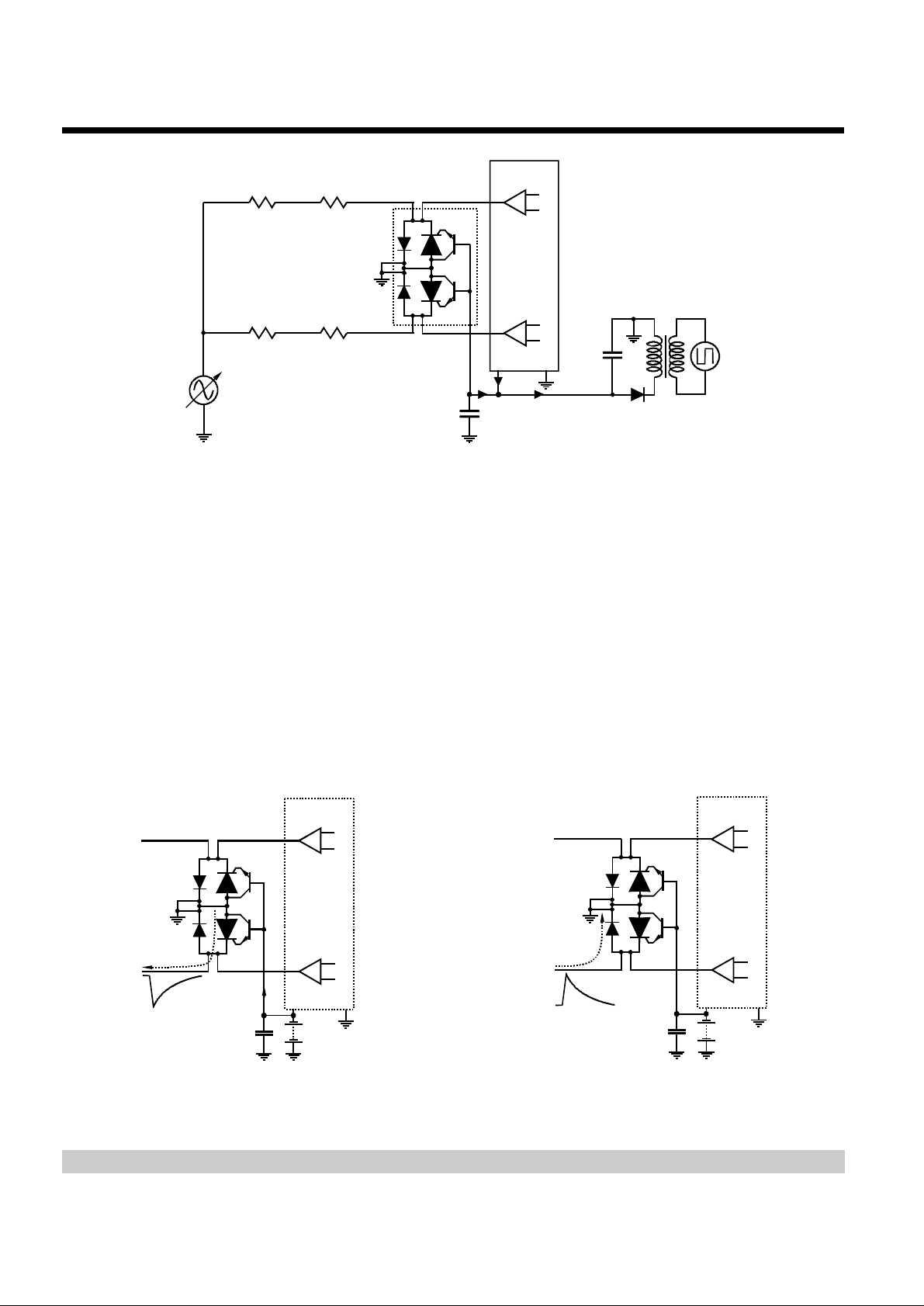
ure 3. TISP61089 BUFFERED GATE PROTECTOR (SECTION 4.5.12 TESTING CONDITION
RING
WIRE
R1a
>25
R1b
>25
Ω
Ω
TISP61089
Th4
Th5
C1
220 nF
SLIC
SWITCHING MODE
POWER SUPPLY
Tx
I
I
SLIC
G
I
BAT
C2
V
BAT
D1
AI6XAG
operation of gated protectors
Figures 4. and 5. show how the TISP61089 limits neg ative and positive overvoltages. Positive overvoltages
(Figure 5) are clipped by the antiparallel diodes in th e TISP61089 and the resulting current is diver ted to
ground. Negative overvoltages (Figure 4.) are initially clipped clos e to the SLIC negative supply rail value
). If sufficient curren t is available from the overvoltage, then the protector (Th5) wil l crowbar into a low
(V
BAT
voltage on-state conditio n. As the overvoltage sub sides th e high holdin g current o f th e crowbar prevents d.c.
latchup. The protection voltage will be th e sum of t he gate su pply (V
(V
). The protection voltage will be i nc reas ed if th er e is a l ong c on necti on bet ween t he gat e d ec oup li ng
GK(BO)
capacitor, C1, and the gate terminal. During the in iti al rise of a fast impulse, the gat e c ur rent (I
as the cathode current (I
). Rates of 70 A/µs can cause inductive voltages of 0.7 V in 2.5 cm of printed wiring
K
) and the peak gate-c athode voltage
BAT
) is the same
G
track. To minimi se this inductive voltage increase of protection voltage, the length of the c apacitor to gate
terminal tracking should be minimised. Inductive voltages in the protector cathode wiring will also increase the
protection voltage. These voltages can be minimised by routing the SLIC connection through the protector as
shown in Figure 3.
PROTECTOR
CROWBAR
OPERATION
I
K
61089
Th5
TISP
C1
220 nF
SLIC
I
G
V
BAT
AI6XAH
PROTECTOR
DIODE
OPERATION
I
F
61089
Th5
TISP
C1
220 nF
SLIC
V
BAT
AI6XAI
Figure 4. NEGATIVE OVERVOLTAGE CONDITION Figure 5. POSITIVE OVERVOLTAGE CONDITION
PRODUCT INFORMATION
6
 Loading...