Power Innovations TISP61089ASDR, TISP61089ASD Datasheet

RINGING SLIC OVERVOLTAGE PROTECTION FOR LSSGR ‘1089
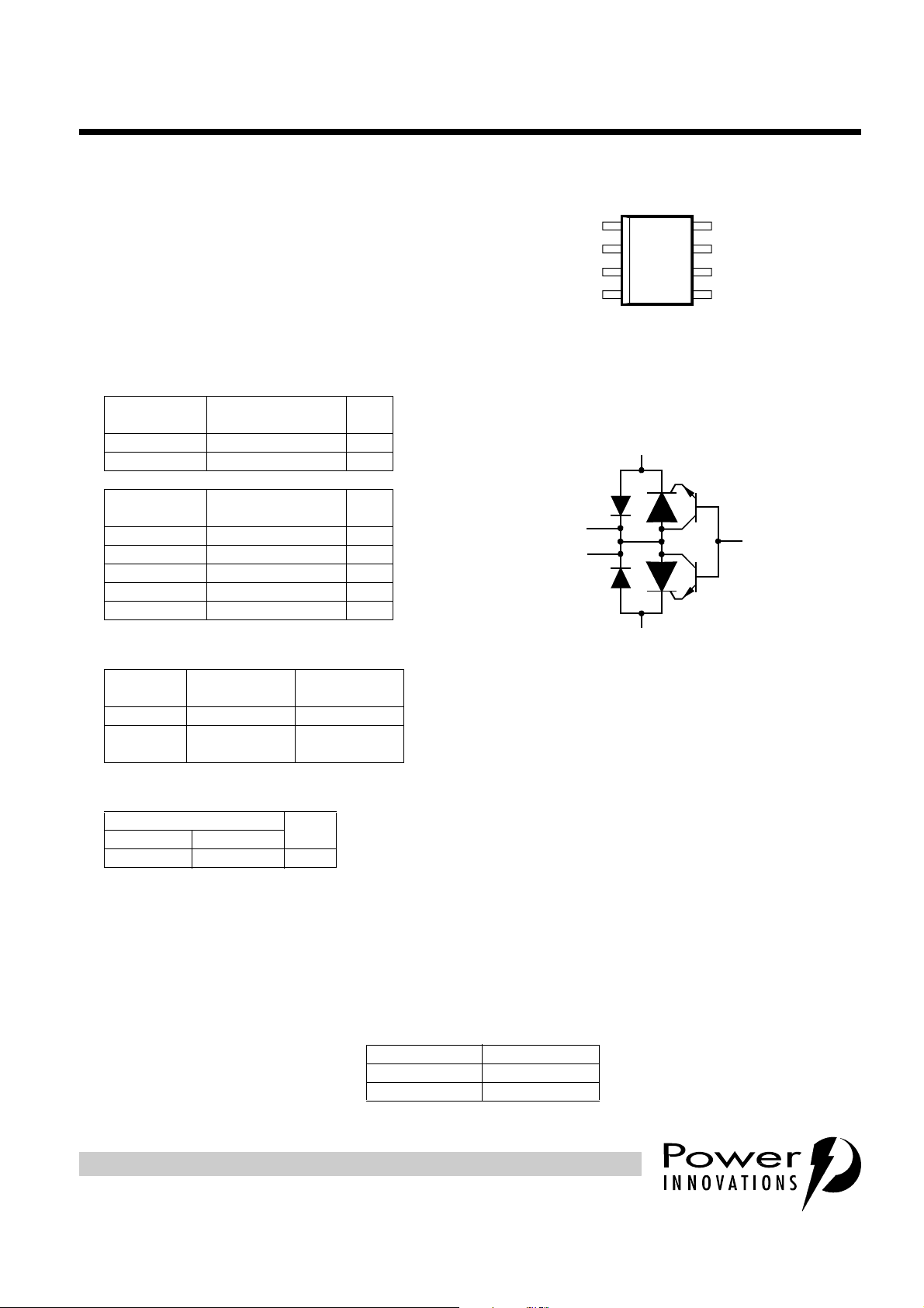
device symbol
●
Dual Voltage-Programmable Protectors
— High Voltage Rating........................-120 V
— Wide Programming Range..... 0 to -100 V
— Low Gate Triggering Current .......< 5 mA
— High Holding Current ................> 150 mA
●
Increased Gound Pin Clearance Version of
TISP61089AD
— Ground Lead Creepage................> 3 mm
— Small Outline Surface Mount Package
●
Rated for LSSGR ‘1089 Conditions
TISP61089AS
DUAL FORWARD-CONDUCTING P-GATE THYRISTORS
PROGRAMMABLE OVERVOLTAGE PROTECTORS
OCTOBER 1999Copyright © 1999, Power Innovations Limited, UK
D PACKAGE
(TOP VIEW)
(Tip)
(Gate)
K1
G
NC
(Ring)
K2
NC - No internal connection
Terminal typical application names shown in
1
2
3
4
parenthesis
8
NC
7
A
(Ground)
6
A
(Ground)
5
NC
MD6XBA
WAVE SHAPE
2/10 µs 4.5.8 Second-Level 1 120
10/1000 µs 4.5.7 First-Level 3 30
60 Hz POWER
FAULT TIME
100 m s 4.5.13 Second-Level 2 11
1 s 4.5.13 Second-Level 2 4.8
5 s 4.5.13 Second-Level 2 2.7
300 s 4.5.13 Second-Level 1 0.95
900 s 4.5.13 Second-Level 1 0.92
●
2/10 Protection Voltage Specified
ELEMENT
Diode 6 8
Crowbar
= -48 V
V
GG
●
Rated for ITU-T K20 & K21 impulses
WAVE SHAPE I
10/700 µs 5/320 40
‘1089 TEST CLAUSE
AND TEST #
‘1089 TEST CLAUSE
AND TEST #
FIRST-LEVEL
V @ 56 A
-57 -60
SECOND-LEVEL
TSP
AVOLTAGE CURRENT
I
TSP
A
I
TSM
A
V @ 100 A
K1
A
A
K2
Termin als K1, K2 and A correspond to the alternative
line designators of T, R and G or A, B and C. The
negative protection voltage is controlled by the
voltage, V
applied to the G terminal.
GG,
G1,G2
SD6XAP
description
PRODUCT INFORMATION
Information is current as of publication date. Products conform to specifications in accordance
with the terms of Power Innovations standard warranty. Production processing does not
necessarily include testing of all parameters.
The TISP61089AS is a dual forward-conducting buffered p-gate overvoltage protector. It is designed to
protect ringing SLICs (Subscr iber L ine Interface Circu its) agains t overvoltages on the tel ephone line cause d
by lightning, a.c. power contact and induction. The TISP61089AS limits voltages that exceed the SLIC supply
rail voltage. The TISP61089AS parameters ar e specified to allow equipm ent compliance with Bel lcore GR1089-CORE, Issue 1.
AVAILABLE OPTIONS
CARRIER ORDER #
Tube TISP61089ASD
Taped and reeled TISP61089ASDR
1

TISP61089AS
DUAL FORWARD-CONDUCTING P-GATE THYRISTORS
PROGRAMMABLE OVERVOLTAGE PROTECTORS
OCTOBER 1999
The SLIC line driver section is typically powered from 0 V (ground) and a negative voltage in the region of
-10 V to -100 V. The protector gate is connected to this negative supply. This references the protection
(clipping) voltage to the nega tive supply voltage. As the prote ction voltage will then track the negative supply
voltage the overvoltage stress on the SLIC is minimised.
Positive over voltages are clipp ed to ground by diode forward conduction. Ne gative overvoltages are initially
clipped close to the SLIC negative supply rail value. If sufficient current is available from the overvoltage, then
the protector will c rowbar in to a l ow voltage on-state cond ition. As the overvoltage sub side s the hi gh hol ding
current of the crowbar prevents d.c. latchup.
The TISP61089AS is inten ded to be used with a series combinati on of a 25Ω or higher re sistance and a
suitable overcurrent protector. Power fault compliance requires the serie s overcurrent element to open- cir cuit
or become high impedance (see Applications Information). For equipment compliant to ITU-T
recommendations K20 or K21 only, the series resistor value is set by the power cross requirements. For K20
and K21, a minimum series resistor value of 10Ω is recommended.
These monolithic prote ction devices are fabricated in ion-implanted planar vertic al power structures for high
reliability and in nor mal system operation they are virtually transparent. The TISP61089AS buffered gate
design reduces the loading on the SLIC supply during overvoltages caused by power cross and induction.
The TISP61089AS is the TISP61089AD with a different pinout. The feed-through Ring (leads 4 — 5) and Tip
(leads 1 — 8) connection s have been replaced by single Ring (lead 4) and Tip (lead 1) connections. This
increases package creepage distance of the biased to ground co nnec ti ons fr om abou t 0.7 mm to over 3 mm.
This increased spacing eases the design task of compliance with various safety standards, such as UL 1950.
absolute maximum ratings
RATING SYMBOL VALUE UNIT
≤
Repetitive peak off-state voltage, I
Repetitive peak gate-cathode voltage, V
Non-repetitive peak on-state pulse current (see Notes 1 and 2)
10/1000 µs (Bellcore GR-1089-CORE, Issue 1, November 1994, Section 4)
5/320 µs (ITU-T recommendation K20 & K21, open-circuit voltage wave shape 10/700)
1.2/50 µs (Bellcore GR-1089-COR E, Issue 1, November 1994, Section 4, Alternative) 100
2/10 µs (Bellcore GR-1089-CORE, Issue 1, November 1994, Section 4) 120
Non-repetitive peak on-state current, V
100 ms 11
1s
5s
300 s
900 s
Non-repetitive peak gate current, 1/2 µs pulse, cathodes commoned (see Notes 1 and 2) I
Operating free-air temperature range T
Junction temperature T
Storage temperature range T
= 0, -40°C≤T
G
= 0, -40°C≤T
KA
= -80 V, 50Hz to 60 Hz (see Notes 1 and 2)
GG
85°C V
J
≤
85°C V
J
DRM
GKRM
I
TSP
I
TSM
GSM
A
J
stg
-120 V
-120 V
30
40
4.8
2.7
0.95
0.92
40 A
-40 to +85 °C
-40 to +150 °C
-65 to +150 °C
A
A
NOTES: 1. Initially the protector must be in thermal equilibrium with -40 °C≤T
its initial conditions.
2. The rated current values may be applied either to the Ring to Ground or to the Tip to Ground terminal pa irs. Additionally, both
terminal pairs may have their rated current values applied simultaneously (in this case the Ground terminal current will be twice the
rated current value of an individual terminal pair). Above 25 °C ambient temperature, derate linearly at -0.6 %/°C. Current values
for other times and gate voltages are shown in Figure 2.
PRODUCT INFORMATION
2
≤
85 °C. The surge may be repeated af ter the device returns to
J

DUAL FORWARD-CONDUCTING P-GATE THYRISTORS
PROGRAMMABLE OVERVOLTAGE PROTECTORS
recommended operating conditions
Gate decoupling capacitor 100 220 nF
C
G
TISP61089AS series resistor for first-level and second-level surge survival
R
S
TISP61089AS series resistor for first-level surge survival
electrical characterist ics, TJ = 25°C (unless otherwise noted)
PARAMETER TEST CONDITIONS MIN TYP M AX UNIT
I
D
V
V
V
I
H
I
GKS
I
GT
V
Q
C
(BO)
F
FRM
GT
GS
AK
Off-state current VD=V
2/10 µs, I
Breakover voltage
2/10 µs, I
1.2/50 µs, I
1.2/50 µs, I
, IG=0
DRM
=-56A, RS=45
T
= -100 A, RS=50
T
= -53 A, RS=47
T
= -96 A, RS=52
T
Ω,
VGG=-48V, CG= 220 nF
Ω,
VGG=-48V, CG= 220 nF
Ω,
VGG=-48V, CG= 220 nF
Ω,
VGG=-48V, CG= 220 nF
Forward voltage IF= 5 A, tw= 200 µs 3V
Ω,
VGG=-48V, CG= 220 nF
Ω,
VGG=-48V, CG= 220 nF
Ω,
VGG=-48V, CG= 220 nF
Ω,
VGG=-48V, CG= 220 nF
Peak forward recovery
voltage
2/10 µs, I
2/10 µs, I
1.2/50 µs, I
1.2/50 µs, I
=56A, RS=45
F
= 100 A , RS=50
F
=53A, RS=47
F
=96A, RS=52
F
Holding current IT= -1 A, di/dt = 1A/ms, VGG= -48 V -150 mA
Gate reverse current VGG=VGK=V
Gate trigger current IT= 3 A, t
Gate trigger voltage IT= 3 A, t
p(g)
p(g)
GKRM
≥
20 µs, V
≥
20 µs, V
, VKA=0
=-48V 5 mA
GG
=-48V 2.5 V
GG
Gate switching charge 1.2/50 µs, IT=53A, RS=47Ω, VGG= -48 V CG= 220 nF 0.1 µC
Anode-cathode off-
state capacitance
f=1MHz, V
=1V, IG= 0, (see Note 3)
d
T
T
T
T
V
V
TISP61089AS
OCTOBER 1999
MIN TYP MAX UNIT
40
25
= 25°C -5 µA
J
= 85°C -50 µA
J
-57
-60
-60
-64
6
8
8
12
= 25°C -5 µA
J
= 85°C -50 µA
J
= -3 V 100 pF
D
=-48V 50 pF
D
Ω
V
V
NOTE 3: These capacitance measurements employ a three terminal capacitance bridge incorporating a guard circuit. The unmeasured
device terminals are a.c. connected to the guard terminal of the bridge.
thermal characteristics
PARAMETER TEST CONDITIONS MIN TYP MAX UNIT
= 25 °C, EIA/JESD51-3 PCB,
T
R
Junction to free air thermal resistance
θ
JA
A
EIA/JESD51-2 environment, I
= I
T
TSM(900)
105 °C/W
PRODUCT INFORMATION
3

TISP61089AS
DUAL FORWARD-CONDUCTING P-GATE THYRISTORS
PROGRAMMABLE OVERVOLTAGE PROTECTORS
OCTOBER 1999
PARAMETER MEASUREMENT INFORMATION
-v
I
(BO)
V
Quadrant III
Switching
Characteristic
V
(BO)
GK(BO)
V
+i
I
(= |I
TSP
|)
FSP
Characteristic
I
(= |I
FSM
GG
I
S
V
S
V
D
|)
TSM
I
F
V
F
I
D
I
H
V
T
I
T
I
TSM
I
TSP
-i
Quadrant I
Forward
Conduction
+v
PM6XAAA
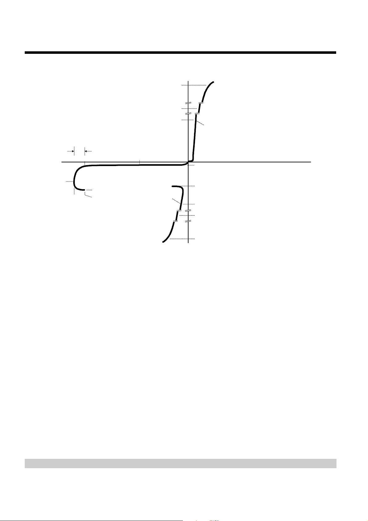
Figure 1. VOLTAGE-CURRENT CHARACTERISTIC
PRODUCT INFORMATION
4

DUAL FORWARD-CONDUCTING P-GATE THYRISTORS
PROGRAMMABLE OVERVOLTAGE PROTECTORS
THERMAL INFORMATION
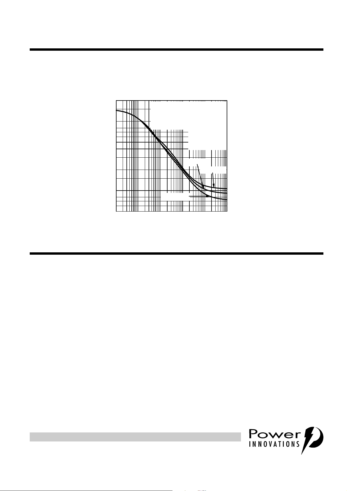
PEAK NON-REPETITIV E ON -ST AT E CURRENT
vs
20
15
10
1.5
CURRENT DURATION
RING AND TIP TERMINALS:
values applied simultaneously
I
TSM
GROUND TERMINAL:
8
7
6
5
4
3
2
Current twice I
value
TSM
EIA /JESD51
Environment and
PCB, T
VGG = -80 V
TI6LAE
= 25 °C
A
VGG = -60 V
TISP61089AS
OCTOBER 1999
1
0.8
0.7
0.6
— Peak Non-Repetitive 50 Hz to 60 Hz Current — A
0.5
TSM
I
0.01 0.1 1 10 100 1000
VGG = -100 V
t — Current Duration — s
Figure 2. NON-REPETITIVE PEAK ON-STATE CURRENT AGAINST DURATION
APPLICATIONS INFORMATION
gated protectors
This section covers three topics. Firstly, it is explained why gated protectors ar e n eed ed. S econd, the voltage
limiting action of the protector is described. Third, an example application circuit is described.
purpose of gated protectors
Fixed voltage thyristor overvoltage protectors have been used since the early 1980s to protect monol ithic
SLICs (Subscriber Line Interface Circuits) against overvoltages on the telephone line caused by lightning, a.c.
power contact and induction. As the SLIC was usually powered from a fixed voltage negative supply rail, the
limiting voltage of the protector could als o be a fixed value. The TISP1072F3 is a typical example of a fixed
voltage SLIC protector.
SLICs have become more sophisticated. To minimise power consumption, some designs automatically adjust
the supply voltage, V
, to a value that is just sufficient to drive the requir ed line curre nt. For shor t lines th e
BAT
supply voltage would be set low, but for long lines, a higher supply voltage would be generated to drive
sufficient line curre nt. The optimum protection for this type of SLIC would be given by a protection voltage
which tracks the SLIC supply voltage. This can be achieved by connecting the protection thyristor ga te to th e
SLIC supply, Figure 3. This gated (programmable) protection arrangement mi nimises the voltage stress on
the SLIC, no matter what value of supply voltage.
PRODUCT INFORMATION
5
 Loading...