Power Innovations TISP5150H3BJ, TISP5080H3BJ, TISP5070H3BJ Datasheet

TISP5070H3BJ, TISP5080H3BJ, TISP5110H3BJ, TISP5150H3BJ
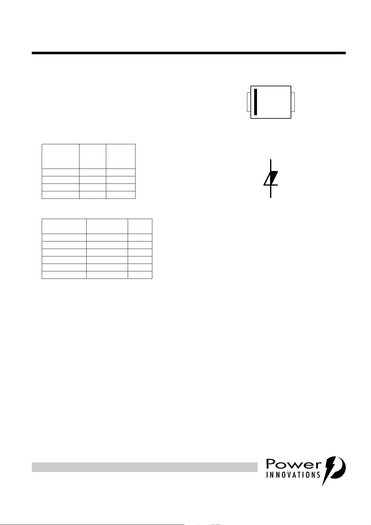
device symbol
SD5XAB
2
1
UNIDIRECTIONAL THYRISTOR OVERVOLTAGE PROTECTORS
TELECOMMUNICATION SYSTEM HIGH CURRENT OVERVOLTAGE PROTECTORS
●
Analogue Line Card and ISDN Protection
- Analogue SLIC
- ISDN U Interface
- ISDN Power Supply
●
8 kV 10/700, 200 A 5/310 ITU-T K20/21 rating
●
Ion-Implanted Breakdown Region
Precise and Stable Voltage
Low Voltage Overshoot under Surge
FORWARD-CONDUCTING
JANUARY 1998 - REVISED MARCH 1999Copyright © 1999, Power Innovations Limited, UK
SMBJ PACKAGE
(TOP VIEW)
12
MDXXBGB
V
DRM
DEVICE
‘5070 -58 -70
‘5080 -65 -80
‘5110 -80 -110
‘5150 -120 -150
●
Rated for International Surge Wave Shapes
WAVE SHAPE STANDARD
2/10 µs GR-1089-CORE 500
8/20 µs ANSI C62.41 300
10/160 µs FCC Par t 68 250
10/700 µs ITU-T K20/21 200
10/560 µs FCC Par t 68 160
10/1000 µs GR-1089-CORE 100
MINIMUM
V
V
(BO)
MAXIMUM
V
I
TSP
A
description
These devices are designed to limit overvoltages on the telephone and data lines. Overvoltages are normally
caused by a.c. power system or lightning flash disturbances which are induced or conducted on to the
telephone line. A single device provides 2-point protection and is typically used for the protection of ISDN
power supply feeds. Two devices, one for the Ring output and the other for the Tip output, will provide
protection for single supply analogue SLICs. A combination of three devices will give a low capacitance
protector network for the 3-point protection of ISDN lines.
PRODUCT INFORMATION
Information is current as of publication date. Products conform to speci fic ations in accordance
with the terms of Power Innovations standard warranty. Production processing does not
necessarily include testing of all parameters.
The protector consists of a voltage-triggered unidirectional thyristor with an anti-parallel diode. Negative
overvoltages are initially clipped by brea kdown clamping until the voltage r ises to the breakover level, which
causes the device to crowbar into a low-voltage on state. This low-voltage on state causes the current
resulting from the overvoltage to be safely diverted through the device. The high crowbar holding current
prevents d.c. latchup as the diver te d cu rrent s ubsides. Positive overvoltages are limi ted by the conduc tion o f
the anti-parallel diode.
This TISP5xxxH3BJ range consists of four voltage variants to meet vari ous maximum sys tem voltage levels
(58 V to 120 V). They are guaranteed to voltage limit and withstand the listed international lightning surges in
both polarities. The se hi gh (H ) c urre nt pr otecti on devices ar e in a pla stic pa ckage SMB J ( JEDE C DO- 21 4AA
with J-bend leads) and supplied in embossed carrier reel pack.
1

TISP5070H3BJ, TISP5080H3BJ, TISP5110H3BJ, TISP5150H3BJ
FORWARD-CONDUCTING
UNIDIRECTIONAL THYRISTOR OVERVOLTAGE PROTECTORS
JANUARY 1998 - REVISED MA RCH 1999
T
absolute maximum ratings,
Repetitive peak off-state voltage, (see Note 1)
Non-repetitive peak on-state pulse current (see Notes 2, 3 and 4)
2/10 µs (GR-1089-CORE, 2/10 µs voltage wave shape) 500
8/20 µs (IEC 61000-4-5, 1.2/50 µs voltage, 8/20 current combination wave generator) 300
10/160 µs (FCC Part 68, 10/160 µs voltage wave shape) 250
5/200 µs (VDE 0433, 10/700 µs voltage wave shape) 220
0.2/310 µs (I3124, 0.5/700 µs voltage wave shape) 200
5/310 µs (ITU-T K20/21, 10/700 µs voltage wave shape) 200
5/310 µs (FTZ R12, 10/700 µs voltage wave shape) 200
10/560 µs (FCC Part 68, 10/560 µs voltage wave shape) 160
10/1000 µs (GR-1089-CORE, 10/1000 µs voltage wave shape) 100
Non-repetitive peak on-state current (see Notes 2, 3 and 5)
20 ms (50 Hz) full sine wave
16.7 ms (60 Hz) full sine wave
1000 s 50 Hz/60 Hz a.c.
Initial rate of rise of on-state current, Exponential current ramp, Maximum ramp value < 140 A di
Junction temperature T
Storage temperature range T
= 25°C (unless otherwise noted)
A
RATING SYMBOL VALUE UNIT
‘5070
‘5080
‘5110
‘5150
- 58
V
DRM
I
TSP
I
TSM
/dt 400 A/µs
T
J
stg
- 65
- 80
-120
55
60
2.1
-40 to +150 °C
-65 to +150 °C
V
A
A
NOTES: 1. See Figure 9 for voltage values at low er temperatures.
2. Initially the TISP5xxxH3BJ must be in thermal equilibrium with T
3. The surge may be repeated after the TISP5xxxH3BJ returns to its initial conditions.
4. See Figure 10 for current ratings at other temperatures.
5. EIA/JESD51-2 environment and EIA/JESD51-3 PCB with standard footprint dimensions connected with 5 A rated printed w iring
track widths. See Figure 8 for the current ratings at other durations. Derat e current v alues at -0.61%/°C for ambient temperatures
above 25 °C
=25°C.
J
electrical characteristics for terminal pair, TA = 25°C (unless otherwise noted)
PARAMETER TEST CONDITIONS MIN TYP MAX UNIT
I
DRM
V
V
I
(BO)
V
V
V
I
H
Repetitive peak offstate current
Breakover voltage dv/dt = -750 V/ms, R
(BO)
Impulse breakover
(BO)
voltage
Breakover current dv/dt = -750 V/ms, R
Forward voltage IF= 5 A, tW= 500 µs ‘5070 thru ‘5150 3 V
F
Peak forward recovery
FRM
voltage
On-state voltage IT=-5A, tW= 500 µs -3 V
T
Holding current IT= -5 A, di/dt = +30 mA/ms -0.15 -0.6 A
V
= V
D
DRM
Ω
= 300
SOURCE
dv/dt≥-1000 V/µs, Linear voltage ramp,
Maximum ramp value = -500 V
di/dt = -20 A/µs, Linear current ramp,
Maximum ramp value = -10 A
Ω
= 300
SOURCE
dv/dt≤+1000 V/µs, Linear voltage ramp,
Maximum ramp value = +500 V
di/dt = +20 A/µs, Linear current ramp,
Maximum ramp value = +10 A
TA = 25°C
T
= 85°C
A
‘5070
‘5080
‘5110
‘5150
‘5070
‘5080
‘5110
‘5150
-0.15 -0.6 A
‘5070 thru ‘5150 5 V
-5
-10
-70
-80
-110
-150
-80
-90
-120
-160
µA
V
V
PRODUCT INFORMATION
2

TISP5070H3BJ, TISP5080H3BJ, TISP5110H3BJ, TISP5150H3BJ
FORWARD-CONDUCTING
UNIDIRECTIONAL THYRISTOR OVERVOLTAGE PROTECTORS
JANUARY 1998 - REVISED MARCH 1999
electrical characteristics for terminal pair, TA = 25°C (unless otherwise noted) (continued)
PARAMETER TEST CONDITIONS MIN TYP MAX UNIT
dv/dt
I
C
Critical rate of rise of
off-state voltage
Off-state current VD=-50V TA = 85°C -10 µA
D
Off-state capacitance
off
Linear voltage ramp, Maximum ramp value< 0.85V
f = 100 kHz, V
(see Note 6)
f = 100 kHz, V
f = 100 kHz, V
f = 100 kHz, V
= 1 Vrms, VD=-1V,
d
= 1 Vrms, VD=-2V
d
= 1 Vrms, VD=-50V
d
= 1 Vrms, VD= -100 V
d
DRM
‘5070
‘5080
‘5110
‘5150
‘5070
‘5080
‘5110
‘5150
‘5070
‘5080
‘5110
‘5150
‘5150
-5 kV/µs
300
280
240
140
260
245
205
120
90
80
65
35
30
420
390
335
195
365
345
285
170
125
110
90
50
40
pF
NOTE 6: Up to 10 MHz the capacitance is essentially independent of frequency. Above 10 MHz the effective capacitance is strongly
dependent on connection inductance.
thermal characteristics
PARAMETER
EIA/JESD51-3 PCB, I
= 25 °C, (see Note 7)
T
R
NOTE 7: EIA/JESD51-2 environment and PCB has standard footprint dimensions connected with 5 A rated printed wiring track widths.
Junction to free air thermal resistance
θ
JA
A
265 mm x 210 mm populated line card,
4-layer PCB, I
TEST CONDITIONS
= I
T
TSM(1000)
= I
T
TSM(1000)
, TA = 25 °C
,
MIN TYP MAX UNIT
113
°C/W
50
PRODUCT INFORMATION
3

TISP5070H3BJ, TISP5080H3BJ, TISP5110H3BJ, TISP5150H3BJ
FORWARD-CONDUCTING
UNIDIRECTIONAL THYRISTOR OVERVOLTAGE PROTECTORS
JANUARY 1998 - REVISED MA RCH 1999
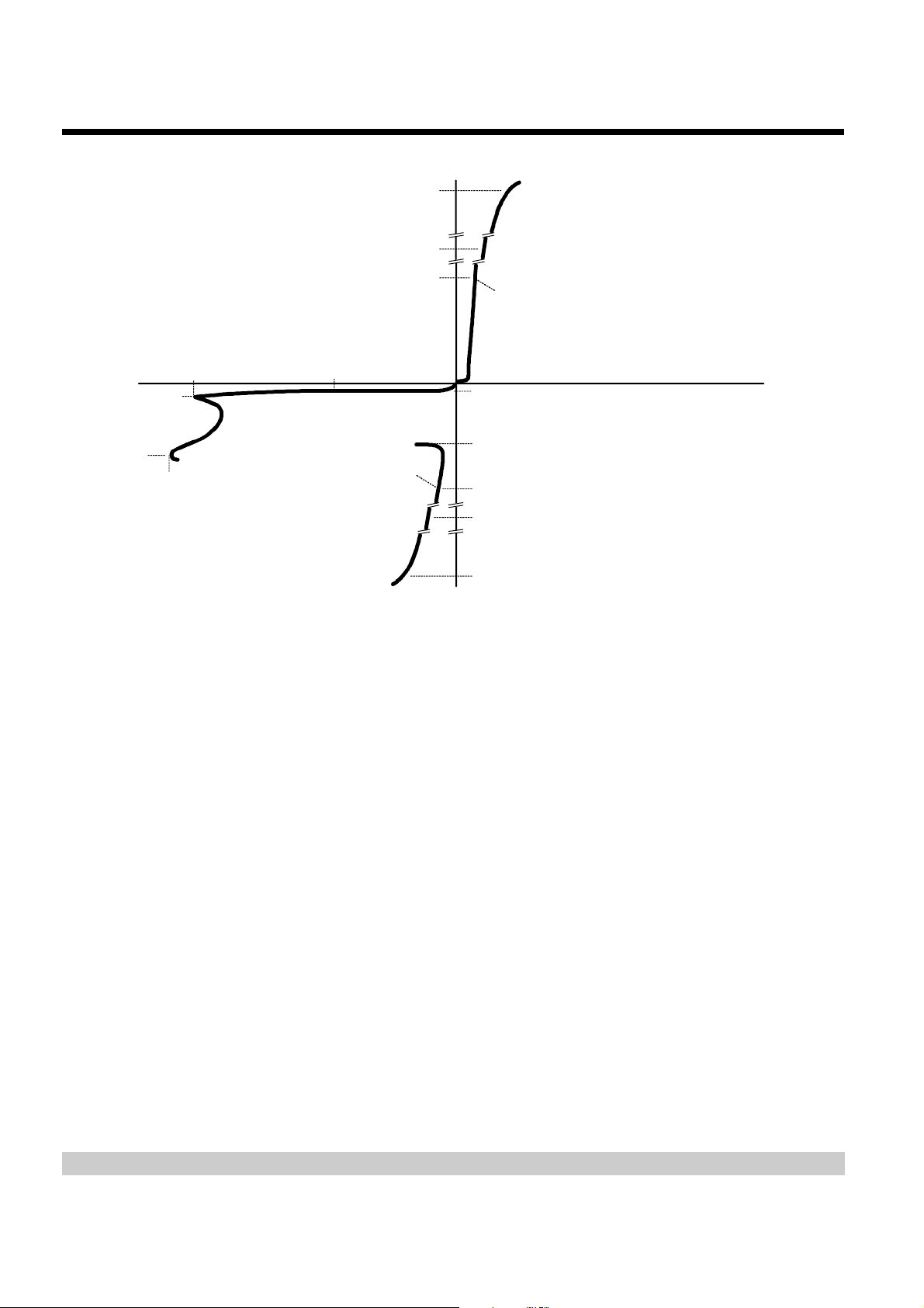
PARAMETER MEASUREMENT INFORMATION
+i
I
TSP
I
TSM
I
F
V
F
Quadrant I
Forward
Conduction
Characteristic
V
-v
I
(BO)
DRM
I
DRM
V
(BO)
Quadrant III
Switching
Characteristic
Figure 1. VOLTAGE-CURRENT CHARACTERISTIC FOR TERMINAL PAIR
V
D
I
D
I
H
V
T
I
T
I
TSM
I
TSP
-i
ALL MEASUREMENTS ARE REFERENCED TO TERMINAL 1
+v
PMXXACA
PRODUCT INFORMATION
4

- Off-State Current - µA
NORMALISED BREAKO V ER VOLTAGE
vs
JUNCTION TEM P ERATURE
TJ - Junction Temperature - °C
-25 0 25 50 75 100 125 150
Normalised Breakover Voltage
0.95
1.00
1.05
1.10
TC5XAIA
NORMALISED HOLDING CURRENT
vs
JUNCTION T EM PERATURE
TJ - Junction Temperature - °C
-25 0 25 50 75 100 125 150
Normalised Holding Current
0.4
0.5
0.6
0.7
0.8
0.9
1.5
2.0
1.0
TC5XAD
D
I
100
10
0·1
0·01
TISP5070H3BJ, TISP5080H3BJ, TISP5110H3BJ, TISP5150H3BJ
FORWARD-CONDUCTING
UNIDIRECTIONAL THYRISTOR OVERVOLTAGE PROTECTORS
JANUARY 1998 - REVISED MARCH 1999
TYPICAL CHARACTERISTICS
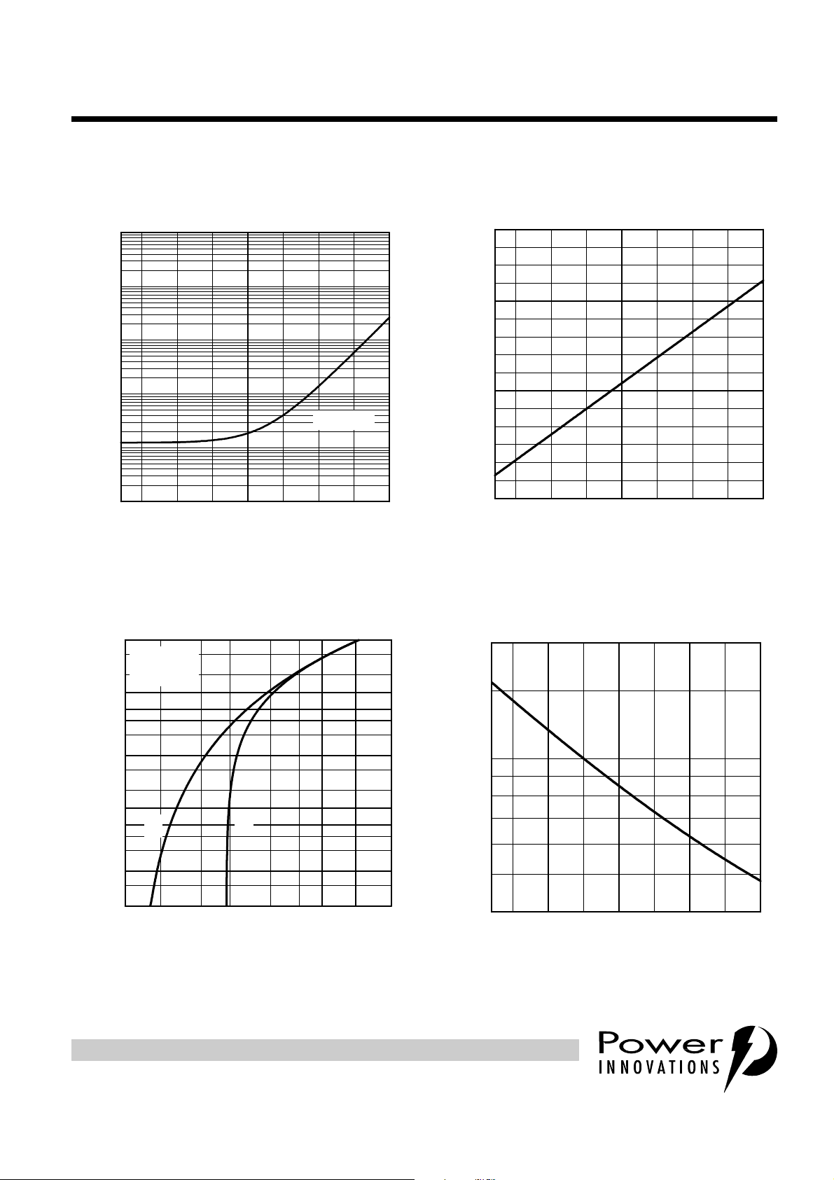
OFF-ST AT E CURRE NT
vs
JUNCTION TEM P ERATURE
1
TC5XAFA
VD = -50 V
0·001
-25 0 25 50 75 100 125 150
T
- Junction Temperature - °C
Figure 2. Figure 3.
ON-STATE AND F ORWARD CURRENTS
vs
ON-STATE AND F ORWARD VOL TAGES
200
150
TA = 25 °C
100
t
= 100 µs
W
70
50
40
30
20
15
10
7
V
5
F
4
3
- On-State Curren t, Forward Current - A
F
2
, I
T
I
1.5
1
0.7 1.5 2 3 4 5 7110
TC5LAC
VT , VF- On-State Voltage, Forward Voltage - V
V
Figure 4. Figure 5.
T
PRODUCT INFORMATION
5
 Loading...