Power Innovations TIC206D, TIC206S, TIC206N, TIC206M Datasheet

● Sensitive Gate Triacs
● 4 A RMS
● Glass Passivated Wafer
● 400 V to 800 V Off-State Voltage
● Max I
of 5 mA (Quadrants 1 - 3)
GT
MT1
MT2
TIC206 SERIES
SILICON TRIACS
DECEMBER 1971 - REVISED MARCH 1997Copyright © 1997, Power Innovations Limited, UK
TO-220 PACKAGE
(TOP VIEW)
1
2
G
3
Pin 2 is in electrical contact with the mounting base.
absolute maximum ratings over operating case temperature (unless otherwise noted)
RATING SYMBOL VALUE UNIT
TIC206D
Repetitive peak off-state voltage (see Note 1)
TIC206M
TIC206S
V
DRM
TIC206N
Full-cycle RMS on-state current at (or below) 85°C case temperature (see Note 2) I
Peak on-state surge current full-sine-wave (see Note 3) I
Peak on-state surge current half-sine-wave (see Note 4) I
Peak gate current I
Peak gate power dissipation at (or below) 85°C case temperature (pulse width
≤ 200 µs) P
Average gate power dissipation at (or below) 85°C case temperature (see Note 5) P
Operating case temperature range T
Storage temperature range T
Lead temperature 1.6 mm from case for 10 seconds T
T(RMS)
TSM
TSM
GM
GM
G(AV)
C
stg
L
NOTES: 1. These values apply bidirectionally for any value of resistance between the gate and Main Terminal 1.
2. This value applies for 50-Hz full-sine-wave operation with resistive load. Above 85°C derate linearly to 110°C case temperature at
the rate of 160 mA/°C.
3. This value applies for one 50-Hz full-sine-wave when the device is operating at (or below) the rated value of on-state current.
Surge may be repeated after the device has returned to original thermal equilibrium. During the surge, gate control may be lost.
4. This value applies for one 50-Hz half-sine-wave when the device is operating at (or below) the rated value of on-state current.
Surge may be repeated after the device has returned to original thermal equilibrium. During the surge, gate control may be lost.
5. This value applies for a maximum averaging time of 20 ms.
400
600
700
800
25 A
30 A
±0.2 A
1.3 W
0.3 W
-40 to +110 °C
-40 to +125 °C
230 °C
MDC2ACA
V
4 A
electrical characteristics at 25°C case temperature (unless otherwise noted)
PARAMETER TEST CONDITIONS
I
DRM
I
GTM
V
GTM
Repetitive peak
off-state current
Peak gate trigger
current
Peak gate trigger
voltage
= rated V
V
D
V
supply
V
supply
V
supply
V
supply
V
supply
V
supply
V
supply
V
supply
DRM
= +12 V†
= +12 V†
= -12 V†
= -12 V†
= +12 V†
= +12 V†
= -12 V†
= -12 V†
IG = 0 TC = 110°C ±1 mA
R
= 10 Ω
L
RL = 10 Ω
RL = 10 Ω
RL = 10 Ω
R
= 10 Ω
L
RL = 10 Ω
RL = 10 Ω
RL = 10 Ω
t
t
t
t
t
t
t
t
p(g)
p(g)
p(g)
p(g)
p(g)
p(g)
p(g)
p(g)
> 20 µs
> 20 µs
> 20 µs
> 20 µs
> 20 µs
> 20 µs
> 20 µs
> 20 µs
† All voltages are with respect to Main Terminal 1.
PRODUCT INFORMATION
Information is current as of publication date. Products conform to specifications in accordance
with the terms of Power Innovations standard warranty. Production processing does not
necessarily include testing of all parameters.
MIN TYP MAX
0.5
-1.5
-2
3.6
0.7
-0.7
-0.8
0.8
5
-5
-5
10
2
-2
-2
2
UNIT
mA
V
1

TIC206 SERIES
SILICON TRIACS
DECEMBER 1971 - REVISED MARCH 1997
electrical characteristics at 25°C case temperature (unless otherwise noted) (continued)
PARAMETER TEST CONDITIONS
V
TM
I
H
I
L
dv/dt
dv/dt
Peak on-state voltage ITM = ±4.2 A IG = 50 mA (see Note 6) ±1.3 ±2.2 V
Holding current
Latching current
Critical rate of rise of
off-state voltage
Critical rise of
(c)
commutation voltage
V
V
V
V
V
V
supply
supply
supply
supply
DRM
DRM
= +12 V†
= -12 V†
= +12 V†
= -12 V†
= Rated V
= Rated V
I
= 0
G
= 0
I
G
(see Note 7)
DRMIG
DRMITRM
= 0 TC = 110°C ±50 V/µs
= ±4.2 A TC = 85°C ±1 ±1.3 ±2.5 V/µs
† All voltages are with respect to Main Terminal 1.
NOTES: 6. This parameter must be measured using pulse techniques, t
the current carrying contacts are located within 3.2 mm from the device body.
7. The triacs are triggered by a 15-V (open circuit amplitude) pulse supplied by a generator with the following characteristics:
= 100 Ω, t
R
G
= 20 µs, tr = ≤ 15 ns, f = 1 kHz.
p(g)
thermal characteristics
PARAMETER MIN TYP MAX UNIT
R
R
Junction to case thermal resistance 7.8 °C/W
θJC
Junction to free air thermal resistance 62.5 °C/W
θJA
MIN TYP MAX
Init’ I
Init’ I
= 100 mA
TM
= -100 mA
TM
2
-4
-15
-30
= ≤ 1 ms, duty cycle ≤ 2 %. Voltage-sensing contacts separate from
p
15
30
UNIT
mA
mA
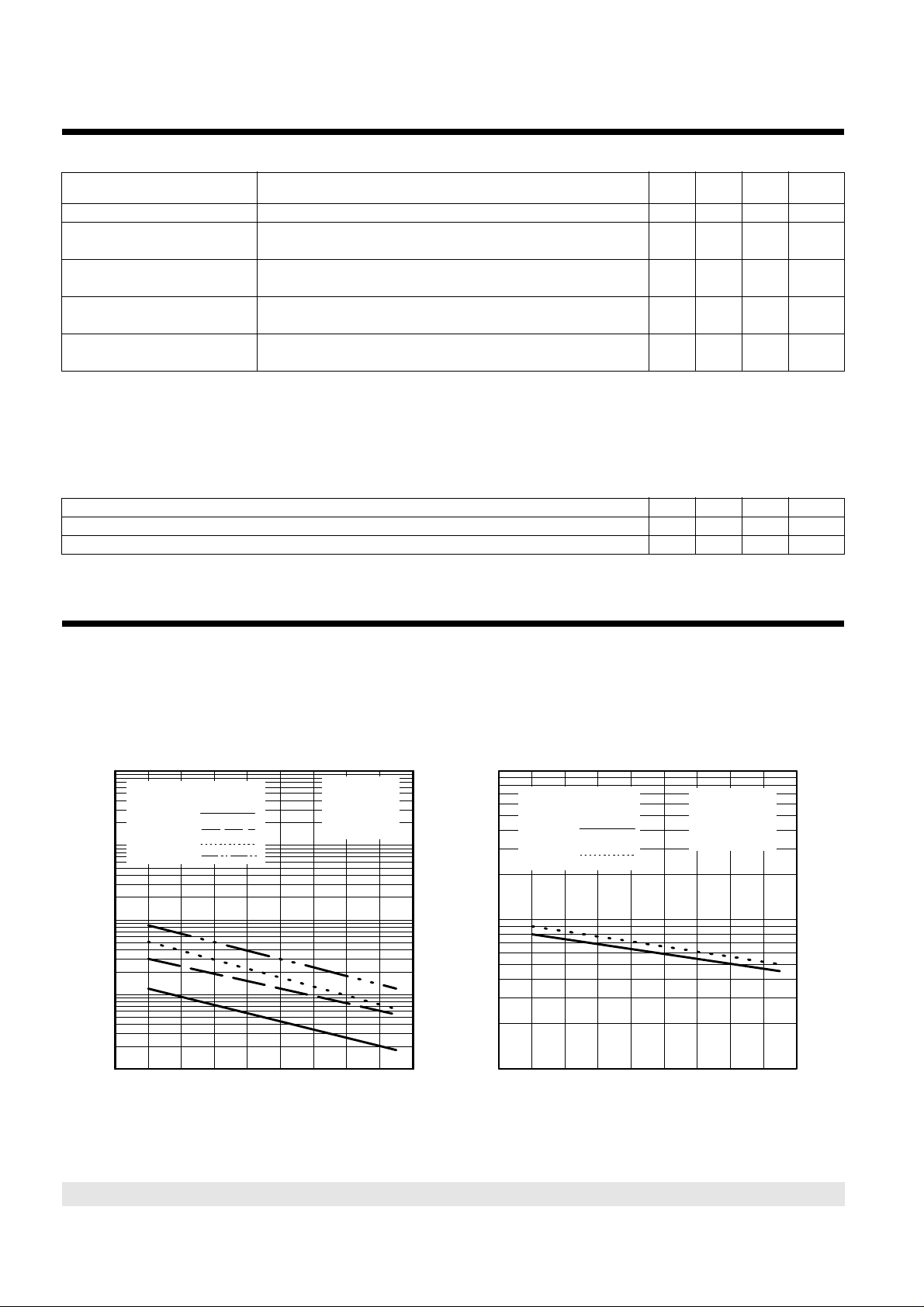
TYPICAL CHARACTERISTICS
GATE TRIGGER CURRENT
vs
TEMPERA TURE
1000
V
supply IGTM
+ +
+ -
100
- -
- +
10
- Gate Trigger Current - mA
GT
1
I
0·1
-60 -40 -20 0 20 40 60 80 100 120
TC - Case Temperature - °C
Figure 1. Figure 2.
VAA = ± 12 V
RL = 10 ΩΩ
t
w(g)
TC05AA
= 20 µs
GATE TRIGGER VOLTAGE
vs
TEMPERATURE
10
V
supply IGTM
+ +
}
+ -
- }
- +
1
- Gate Trigger Voltage - V
GT
V
0·1
-60 -40 -20 0 20 40 60 80 100 120
TC - Case Temperature - °C
VAA = ± 12 V
RL = 10 ΩΩ
t
= 20 µs
w(g)
TC05AB
PRODUCT INFORMATION
2
 Loading...