● 5 A Continuous On-State Current
● 30 A Surge-Current
● Glass Passivated Wafer
● 400 V to 800 V Off-State Voltage
● Max I
of 200 µA
GT
TIC106 SERIES
SILICON CONTROLLED RECTIFIERS
APRIL 1971 - REVISED MARCH 1997Copyright © 1997, Power Innovations Limited, UK
TO-220 PACKAGE
(TOP VIEW)
K
A
G
1
2
3
Pin 2 is in electrical contact with the mounting base.
absolute maximum ratings over operating case temperature (unless otherwise noted)
RATING SYMBOL VALUE UNIT
TIC106D
Repetitive peak off-state voltage (see Note 1)
Repetitive peak reverse voltage
Continuous on-state current at (or below) 80°C case temperature (see Note 2) I
Average on-state current (180° conduction angle) at (or below) 80°C case temperature
(see Note 3)
Surge on-state current (see Note 4) I
Peak positive gate current (pulse width
Peak gate power dissipation (pulse width
Average gate power dissipation (see Note 5) P
Operating case temperature range T
Storage temperature range T
Lead temperature 1.6 mm from case for 10 seconds T
NOTES: 1. These values apply when the gate-cathode resistance RGK = 1 kΩ.
2. These values apply for continuous dc operation with resistive load. Above 80°C derate linearly to zero at 110°C.
3. This value may be applied continuously under single phase 50 Hz half-sine-wave operation with resistive load. Above 80°C derate
linearly to zero at 110°C.
4. This value applies for one 50 Hz half-sine-wave when the device is operating at (or below) the rated value of peak reverse voltage
and on-state current. Surge may be repeated after the device has returned to original thermal equilibrium.
5. This value applies for a maximum averaging time of 20 ms.
≤ 300 µs) I
≤ 300 µs) P
TIC106M
TIC106S
TIC106N
TIC106D
TIC106M
TIC106S
TIC106N
V
DRM
V
RRM
T(RMS)
I
T(AV)
TM
GM
GM
G(AV)
C
stg
L
400
600
700
800
400
600
700
800
3.2 A
30 A
0.2 A
1.3 W
0.3 W
-40 to +110 °C
-40 to +125 °C
230 °C
MDC1ACA
V
V
5 A
PRODUCT INFORMATION
Information is current as of publication date. Products conform to specifications in accordance
with the terms of Power Innovations standard warranty. Production processing does not
necessarily include testing of all parameters.
1

TIC106 SERIES
SILICON CONTROLLED RECTIFIERS
APRIL 1971 - REVISED MARCH 1997
electrical characteristics at 25°C case temperature (unless otherwise noted)
PARAMETER TEST CONDITIONS MIN TYP MAX UNIT
I
I
dv/dt
Repetitive peak
DRM
off-state current
Repetitive peak
RRM
reverse current
Gate trigger current VAA = 6 V RL= 100 Ω t
I
GT
Gate trigger voltage
V
GT
Holding current
I
H
Peak on-state
V
TM
voltage
Critical rate of rise of
off-state voltage
NOTE 6: This parameter must be measured using pulse techniques, tp = 300 µs, duty cycle ≤ 2 %. Voltage sensing-contacts, separate from
the current carrying contacts, are located within 3.2 mm from the device body.
= rated V
V
D
= rated V
V
R
V
= 6 V
AA
≥ 20 µs
t
p(g)
= 6 V
V
AA
≥ 20 µs
t
p(g)
= 6 V
V
AA
≥ 20 µs
t
p(g)
V
= 6 V
AA
Initiating I
= 6 V
V
AA
Initiating I
= 5 A (See Note 6) 1.7 V
I
TM
= rated V
V
D
DRM
RRM
= 10 mA
T
= 10 mA
T
D
RGK = 1 kΩ TC = 110°C 400 µA
IG = 0 TC = 110°C 1 mA
≥ 20 µs 60 200 µA
R
= 100 Ω
L
RGK= 1 kΩ
R
= 100 Ω
L
RGK= 1 kΩ
R
= 100 Ω
L
RGK= 1 kΩ
R
= 1 kΩ TC = - 40°C
GK
R
= 1 kΩ
GK
p(g)
TC = - 40°C
TC = 110°C
1.2
0.4 0.6 1
0.2
8
5
RGK= 1 kΩ TC = 110°C 10 V/µs
V
mA
thermal characteristics
PARAMETER MIN TYP MAX UNIT
R
R
Junction to case thermal resistance 3.5 °C/W
θJC
Junction to free air thermal resistance 62.5 °C/W
θJA
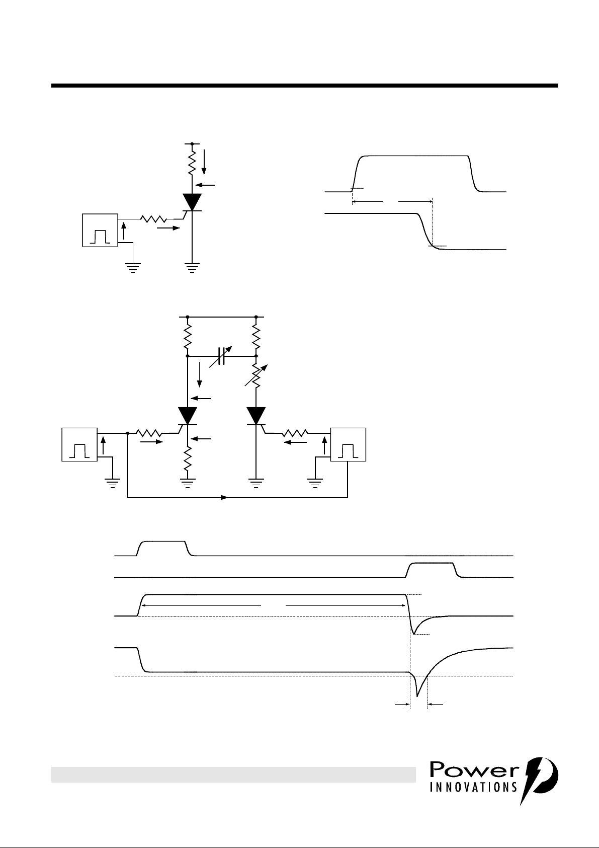
resistive-load-switching characteristics at 25°C case temperature
PARAMETER TEST CONDITIONS MIN TYP MAX UNIT
Gate-controlled
t
gt
turn-on time
Circuit-commutated
t
q
turn-off time
= 5 A IG = 10 mA See Figure 1 1.75 µs
I
T
IT = 5 A
= 8 A
I
RM
I
= 10 mA See Figure 2
G
7.7 µs
PRODUCT INFORMATION
2

TIC106 SERIES
30 V
SILICON CONTROLLED RECTIFIERS
APRIL 1971 - REVISED MARCH 1997
PARAMETER MEASUREMENT INFORMATION
I
ΩΩ
6
R
G
G
V
G
I
G
T
V
V
A
G
10%
DUT
V
A
Figure 1. Gate-controlled turn-on time
30 V
t
gt
90%
PMC1AA
G1
ΩΩ
6
0.1 µµF
to 0.5 µµF
R2
NOTES: A. Resistor R1 is adjusted for the specified value
of IRM.
B. Resistor R2 value is 30/IH, where IH is the
I
A
R1
holding current value of thyristor TH1.
C. Thyristor TH1 is the same device type as the
DUT.
V
A
ΩΩ
DUT
V
K
(IRM Monitor)
R
G
V
G1
I
G
0.1
TH1
R
G
I
G
D. Pulse Generators, G1 and G2, are
synchronised to produce an on-state anode
current waveform with the following
characteristics:
tP = 50 µs to 300 µs
G2
duty cycle = 1%
V
G2
E. Pulse Generators, G1 and G2, have output
pulse amplitude, VG, of ≥ 20 V and duration of
10 µs to 20 µs.
G2 tP Synchronisation
V
G1
V
G2
I
I
A
t
P
T
0
I
RM
V
A
V
Figure 2. Circuit-commutated turn-off time
PRODUCT INFORMATION
T
0
t
q
PMC1AB
3
 Loading...