


Power Innovations BUV47 Datasheet
BUV47, BUV47A
NPN SILICON POWER TRANSISTORS
AUGUST 1978 - REVISED MARCH 1997Copyright © 1997, Power Innovations Limited, UK
● Rugged Triple-Diffused Planar Construction
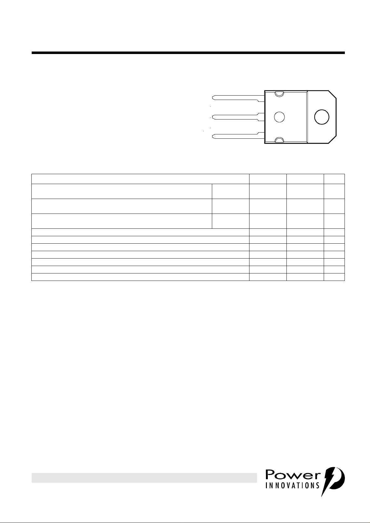
SOT-93 PACKAGE
● 9 A Continuous Collector Current
● 1000 Volt Blocking Capability
B
C
E
(TOP VIEW)
1
2
3
Pin 2 is in electrical contact with the mounting base.
absolute maximum ratings at 25°C case temperature (unless otherwise noted)
RATING SYMBOL VALUE UNIT
Collector-emitter voltage (V
Collector-emitter voltage (R
Collector-emitter voltage (I
= -2.5 V)
BE
= 10 Ω)
BE
= 0)
B
Continuous collector current I
Peak collector current (see Note 1) I
Continuous base current I
Peak base current I
Continuous device dissipation at (or below) 25°C case temperature P
Operating junction temperature range T
Storage temperature range T
NOTE 1: This value applies for tp ≤ 5 ms, duty cycle ≤ 2%.
BUV47
BUV47A
BUV47
BUV47A
BUV47
BUV47A
V
V
V
CEX
CER
CEO
C
CM
B
BM
tot
j
stg
MDTRAA
850
1000
850
1000
400
450
9 A
15 A
3 A
6 A
120 W
-65 to +150 °C
-65 to +150 °C
V
V
V
PRODUCT INFORMATION
Information is current as of publication date. Products conform to specifications in accordance
with the terms of Power Innovations standard warranty. Production processing does not
necessarily include testing of all parameters.
1
BUV47, BUV47A
NPN SILICON POWER TRANSISTORS
AUGUST 1978 - REVISED MARCH 1997
electrical characteristics at 25°C case temperature (unless otherwise noted)
PARAMETER TEST CONDITIONS MIN TYP MAX UNIT
V
CEO(sus)
V
(BR)EBO
I
CES
I
CER
I
EBO
V
CE(sat)
V
BE(sat)
C
Collector-emitter
sustaining voltage
Base-emitter
breakdown voltage
Collector-emitter
cut-off current
Collector-emitter
cut-off current
Emitter cut-off
current
Collector-emitter
saturation voltage
Base-emitter
saturation voltage
Current gain
f
t
bandwidth product
Output capacitance VCB = 20 V IC= 0 f = 0.1 MHz 105 pF
ob
= 200 mA L = 25 mH (see Note 2)
I
C
= 50 mA IC= 0 (see Note 3) 7 30 V
I
E
V
= 850 V
CE
= 1000 V
V
CE
= 850 V
V
CE
= 1000 V
V
CE
V
= 850 V
CE
= 1000 V
V
CE
= 850 V
V
CE
= 1000 V
V
CE
= 5 V IC= 0 1 mA
V
EB
IB = 1 A
= 2.5 A
I
B
= 1 A IC= 5 A (see Notes 3 and 4) 1.6 V
I
B
= 10 V IC= 0.5 A f = 1 MHz 8 MHz
V
CE
NOTES: 2. Inductive loop switching measurement.
3. These parameters must be measured using pulse techniques, t
4. These parameters must be measured using voltage-sensing contacts, separate from the current carrying contacts.
V
= 0
BE
= 0
V
BE
= 0
V
BE
= 0
V
BE
R
= 10 Ω
BE
RBE= 10 Ω
RBE= 10 Ω
RBE= 10 Ω
I
= 5 A
C
= 8 A
I
C
T
= 125°C
C
= 125°C
T
C
TC = 125°C
= 125°C
T
C
(see Notes 3 and 4)
= 300 µs, duty cycle ≤ 2%.
p
BUV47
BUV47A
BUV47
BUV47A
BUV47
BUV47A
BUV47
BUV47A
BUV47
BUV47A
400
450
0.15
0.15
1.5
1.5
0.4
0.4
3.0
3.0
1.5
3.0
V
mA
mA
V
thermal characteristics
PARAMETER MIN TYP MAX UNIT
R
Junction to case thermal resistance 1 °C/W
θJC
resistive-load-switching characteristics at 25°C case temperature
PARAMETER TEST CONDITIONS
Turn on time
t
on
Storage time 3.0 µs
t
s
Fall time 0.8 µs
t
f
†
Voltage and current values shown are nominal; exact values vary slightly with transistor parameters.
I
C
V
CC
= 5 A
= 150 V
I
= 1 A
B(on)
(see Figures 1 and 2)
†
I
= -1 A
B(off)
MIN TYP MAX UNIT
1.0 µs
inductive-load-switching characteristics at 25°C case temperature (unless otherwise noted)
PARAMETER TEST CONDITIONS
Voltage storage time IC = 5 A
t
sv
Current fall time 0.4 µs
t
fi
= 100°C
T
C
I
= 1 A
B(on)
(see Figures 3 and 4)
†
V
= -5 V 4.0 µs
BE(off)
MIN TYP MAX UNIT
PRODUCT INFORMATION
2
NPN SILICON POWER TRANSISTORS
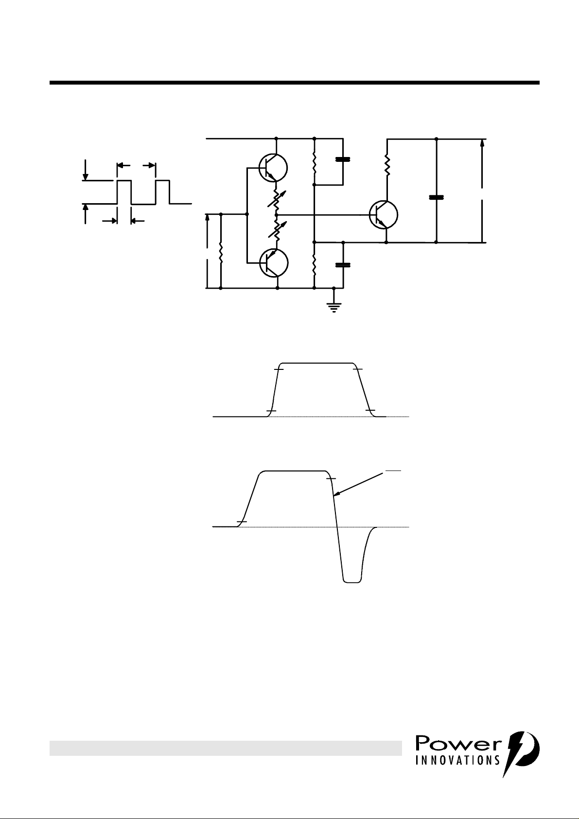
= 15 V, Source Impedance = 50
AUGUST 1978 - REVISED MARCH 1997
PARAMETER MEASUREMENT INFORMATION
+25 V
BUV47, BUV47A
V
1
t
p
tp = 20 µs
Duty cycle = 1%
V
1
A - B = t
d
B - C = t
r
E - F = t
f
D - E = t
s
A - C = t
on
D - F = t
off
BD135
T
V
100
1
Ω
ΩΩ
BD136
47
15
120
ΩΩ
ΩΩ
82
ΩΩ
ΩΩ
µµ
680 F
680 F
µµ
100
ΩΩ
100
TUT
V
V
= 250 V
CC
F
µµ
cc
Figure 1. Resistive-Load Switching Test Circuit
90%
90%
C
I
C
10%
B
90%
I
B
A
10%
E
10%
F
D
I
B(on)
dI
dt
B
≥ 2 A/µs
0%
0%
Figure 2. Resistive-Load Switching Waveforms
PRODUCT INFORMATION
I
B(off)
3