

● Rugged Triple-Diffused Planar Construction
● 100 W at 25°C Case Temperature
● 5 A Continuous Collector Current
NPN SILICON POWER TRANSISTOR
MAY 1989 - REVISED MARCH 1997Copyright © 1997, Power Innovations Limited, UK
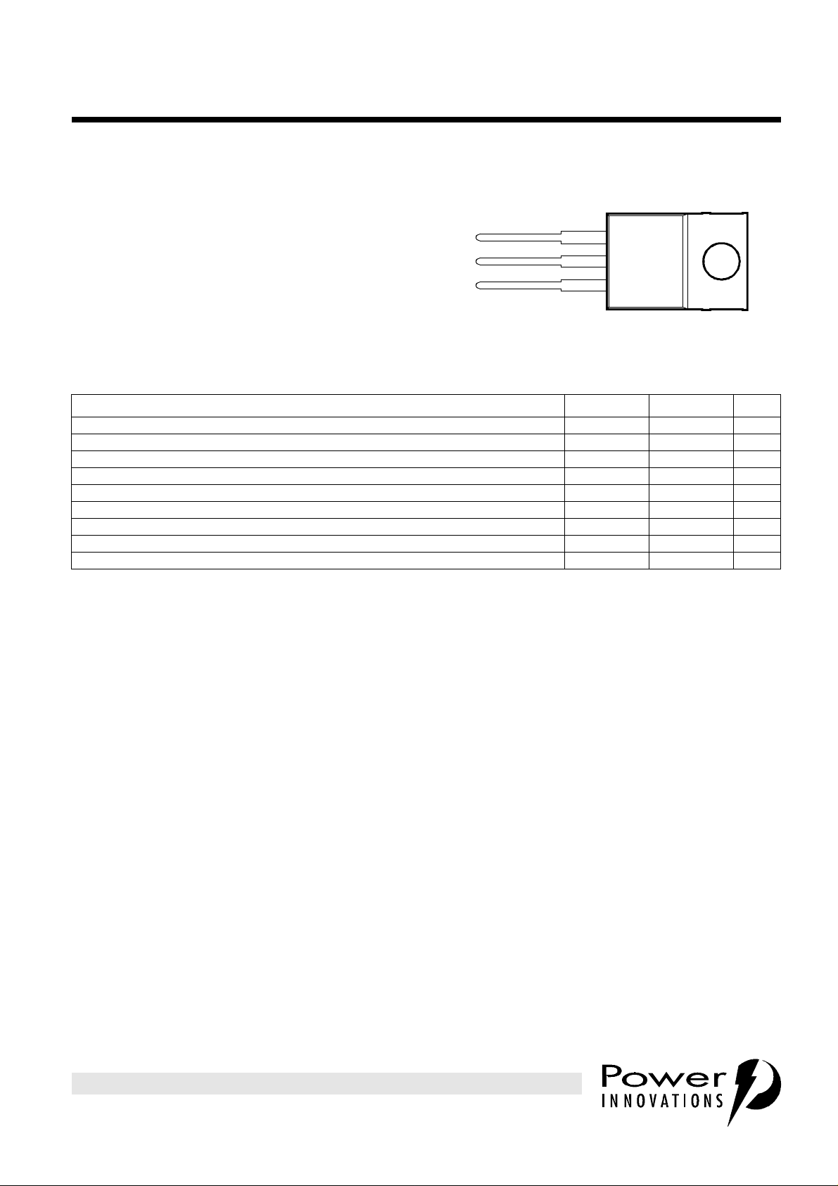
TO-220 PACKAGE
(TOP VIEW)
B
C
E
1
2
3
BUT11
Pin 2 is in electrical contact with the mounting base.
absolute maximum ratings at 25°C case temperature (unless otherwise noted)
RATING SYMBOL VALUE UNIT
Collector-base voltage (I
Collector-emitter voltage (V
Collector-emitter voltage (I
Emitter-base voltage V
Continuous collector current I
Peak collector current (see Note 1) I
Continuous device dissipation at (or below) 25°C case temperature P
Operating junction temperature range T
Storage temperature range T
NOTE 1: This value applies for tp ≤ 10 ms, duty cycle ≤ 2%.
= 0) V
E
= 0) V
BE
= 0) V
B
CBO
CES
CEO
EBO
C
CM
tot
j
stg
MDTRACA
850 V
850 V
400 V
10 V
5 A
10 A
100 W
-65 to +150 °C
-65 to +150 °C
PRODUCT INFORMATION
Information is current as of publication date. Products conform to specifications in accordance
with the terms of Power Innovations standard warranty. Production processing does not
necessarily include testing of all parameters.
1
BUT11
NPN SILICON POWER TRANSISTOR
MAY 1989 - REVISED MARCH 1997
electrical characteristics at 25°C case temperature (unless otherwise noted)
PARAMETER TEST CONDITIONS MIN TYP MAX UNIT
V
CEO(sus)
I
CES
I
EBO
h
V
CE(sat)
V
BE(sat)
C
Collector-emitter
sustaining voltage
Collector-emitter
cut-off current
Emitter cut-off
current
Forward current
FE
transfer ratio
Collector-emitter
saturation voltage
Base-emitter
saturation voltage
Current gain
f
t
bandwidth product
Output capacitance VCB = 20 V IE= 0 f = 0.1 MHz 110 pF
ob
NOTES: 2. Inductive loop switching measurement.
3. These parameters must be measured using pulse techniques, t
4. These parameters must be measured using voltage-sensing contacts, separate from the current carrying contacts.
= 0.1 A L = 25 mH (see Note 2) 400 V
I
C
VCE= 850 V
= 850 V
V
CE
= 10 V IC= 0 1 mA
V
EB
= 5 V IC= 0.5 A (see Notes 3 and 4) 20 60
V
CE
= 0.6 A IC= 3 A (see Notes 3 and 4) 1.5 V
I
B
= 0.6 A IC= 3 A (see Notes 3 and 4) 1.3 V
I
B
= 10 V IC= 0.5 A f = 1 MHz 12 MHz
V
CE
V
= 0
BE
= 0 TC = 125°C
V
BE
= 300 µs, duty cycle ≤ 2%.
p
50
500
µA
thermal characteristics
PARAMETER MIN TYP MAX UNIT
R
Junction to case thermal resistance 1.25 °C/W
θJC
inductive-load-switching characteristics at 25°C case temperature (unless otherwise noted)
PARAMETER TEST CONDITIONS
Voltage storage time IC = 3 A
t
sv
Current fall time 150 ns
t
fi
Voltage storage time IC = 3 A
t
sv
Current fall time 300 ns
t
fi
†
Voltage and current values shown are nominal; exact values vary slightly with transistor parameters.
V
V
CC
CC
= 50 V
= 50 V
I
= 0.6A
B(on)
(see Figures 1 and 2)
I
= 0.6A
B(on)
= 100°C
T
C
†
V
= -5 V 1.4 µs
BE(off)
V
= -5 V 1.5 µs
BE(off)
MIN TYP MAX UNIT
PRODUCT INFORMATION
2
 Loading...