

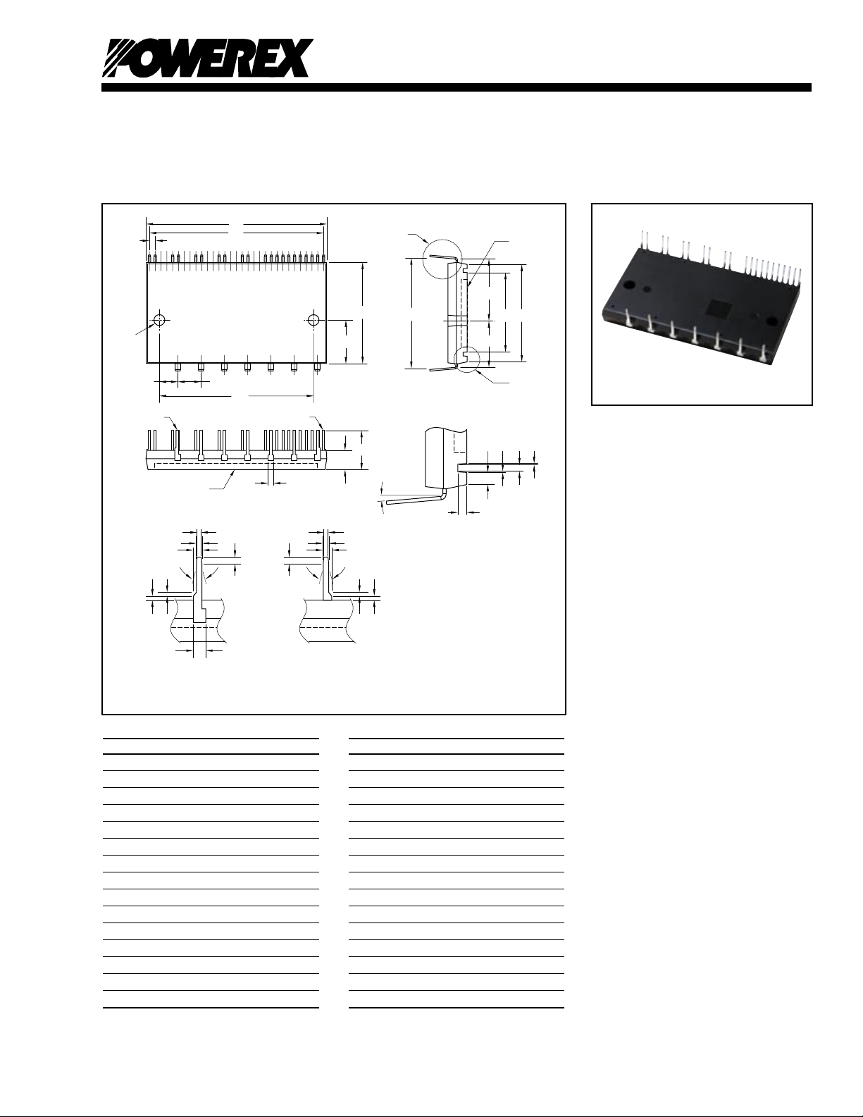
PS22053
0 ~ 5°
LABEL
HEATSINK
SIDE
HEATSINK SIDE
L
B
G
J
E
F
H
R
ALL TERMINALS TREATED BY Pb-FREE SOLDER PLATING
U
SR T S
D
K
O
N
M
C
P
Q
Z
30° 30°
Z A
AAA
BB
LEADS THICKNESS = 0.7mm
Y E
E
V V
W
X
CC
DD
A
17161514
13121110987654321
25 26 27 28242322
212019
1
8
1 VUFS
2 VUFB
3 VP1
4 UP
5 VVFS
6 VVFB
7 VP1
8 VP
9 VWFS
10 VWFB
11 VP1
12 VPC
13 WP
14 VN1
15 VNC
16 CIN
17 CFO
18 FO
19 UN
20 VN
21 WN
22 P
23 U
24 V
25 W
26 NU
27 NV
28 NW
TERMINAL CODE
DETAIL "C"
DETAIL "B"
DETAIL "B" DETAIL "C"
DETAIL "A"
DETAIL "A"
DETAIL "A"
Powerex, Inc., 200 E. Hillis Street, Youngwood, Pennsylvania 15697-1800 (724) 925-7272
Outline Drawing and Circuit Diagram
Dimensions Inches Millimeters
A 3.11±0.02 79.0±0.5
B 1.73±0.02 44.0±0.5
C 0.63±0.01 16.1±0.3
D 3.0 76.2
E 1.08±0.02 27.4±0.5
F 0.80±0.02 20.4±0.5
G 1.91±0.02 48.6±0.5
H 1.34±0.02 34.0±0.5
J 1.67±0.02 42.5±0.5
K 0.10±0.01 2.54±0.3
L 0.73±0.02 18.5±0.5
M 0.31±0.01 8.0±0.3
N 2.64±0.01 67.0±0.3
O 0.40±0.01 10.16±0.3
P 0.32±0.02 8.2±0.5
Intellimod™ Module
Dual-In-Line Intelligent
Power Module
10 Amperes/1200 Volts
Description:
DIP-IPMs are intelligent power
modules that integrate power
devices, drivers, and protection
circuitry in an ultra compact
dual-in-line transfer-mold package
for use in driving small three
phase motors. Use of 4th
generation IGBTs, DIP packaging,
and application specific HVICs
allow the designer to reduce
inverter size and overall design
time.
Dimensions Inches Millimeters
Q 0.09 2.5
R 0.08 2.0
S 0.01 0.3
T 0.07 1.7
U 0.18±0.008 Dia. 4.5±0.2 Dia.
V 0.024 0.6
W 0.039±0.008 1.0±0.2
X 0.06±0.008 1.5±0.2
Y 0.05 1.2
Z 0.02 0.5
AA 0.024±0.02 0.6±0.5
BB 0.098 2.5
CC 0.031±0.008 0.8±0.2
DD 0.051±0.008 1.3±0.2
EE 0.04 1.0
Features:
£ Compact Packages
£ Single Power Supply
£ Integrated HVICs
£ Direct Connection to CPU
Applications:
£ Washing Machines
£ Refrigerators
£ Air Conditioners
£ Small Servo Motors
£ Small Motor Control
Ordering Information:
PS22053 is a 1200V, 10 Ampere
DIP Intelligent Power Module.
1Rev. 10/05
Powerex, Inc., 200 E. Hillis Street, Youngwood, Pennsylvania 15697-1800 (724) 925-7272
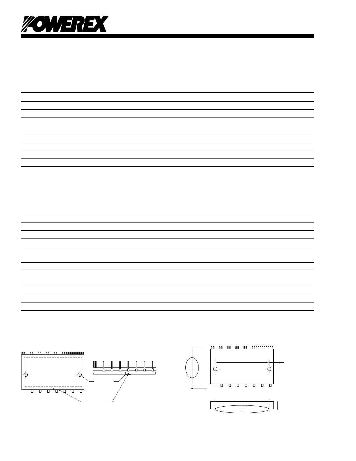
TC POINT
POWER TERMINALS
CONTROL TERMINALS
HEATSINK
BOUNDARY
HEATSINK
MEASUREMENT POINT
3.25mm
HEATSINK
–
+
–
+
PS22053
Intellimod™ Module
Dual-In-Line Intelligent Power Module
10 Amperes/1200 Volts
Absolute Maximum Ratings, Tj = 25°C unless otherwise specified
Characteristics Symbol PS22053 Units
Power Device Junction Temperature* Tj -20 to 125 °C
Module Case Operation Temperature (See Note 1) TC -20 to 100 °C
Storage Temperature T
-40 to 125 °C
stg
Mounting Torque, M4 Mounting Screws — 13 in-lb
Module Weight (Typical) — 77 Grams
Self-protection Supply Voltage Limit (Short Circuit Protection Capability)** V
800 Volts
CC(prot.)
Heatsink Flatness (See Note 2) -50 to 100 µm
Isolation Voltage, AC 1 minute, 60Hz Sinusoidal, Connection Pins to Heatsink Plate V
*The maximum junction temperature rating of the power chips integrated within the DIP-IPM is 150°C (@TC ≤ 100°C). However, to ensure safe operation of the DIP-IPM,
the average junction temperature should be limited to T
**VD = 13.5 ~ 16.5V, Inverter Part, Tj = 125°C, Non-repetitive, Less than 2µs
≤ 125°C (@TC ≤ 100°C).
j(avg)
2500 Volts
ISO
IGBT Inverter Sector
Collector-Emitter Voltage V
Collector Current (TC = 25°C) ±IC 10 Amperes
Peak Collector Current (TC = 25°C, <1ms) ±ICP 20 Amperes
Supply Voltage (Applied between P-NU, NV, NW) VCC 900 Volts
Supply Voltage, Surge (Applied between P-NU, NV, NW) V
Collector Dissipation (TC = 25°C, per 1 Chip) PC 40 Watts
1200 Volts
CES
CC(surge)
1000 Volts
Control Sector
Supply Voltage (Applied between VP1-VPC, VN1-VNC) VD 20 Volts
Supply Voltage (Applied between V
Input Voltage (Applied between UP, VP, WP-VPC, UN, VN, WN-VNC) VIN -0.5 ~ VD+0.5 Volts
Fault Output Supply Voltage (Applied between FO-VNC) VFO -0.5 ~ VD+0.5 Volts
Fault Output Current (Sink Current at FO Terminal) IFO 1 mA
Current Sensing Input Voltage (Applied between CIN-VNC) VSC -0.5 ~ VD+0.5 Volts
Note 1 – TC Measure Point Note 2 – Flatness Measurement Position
UFB-VUFS, VVFB-VVFS
, V
WFB-VWFS
) VDB 20 Volts
2 Rev. 10/05

Powerex, Inc., 200 E. Hillis Street, Youngwood, Pennsylvania 15697-1800 (724) 925-7272
PS22053
Intellimod™ Module
Dual-In-Line Intelligent Power Module
10 Amperes/1200 Volts
Electrical and Mechanical Characteristics, Tj = 25°C unless otherwise specified
Characteristics Symbol Test Conditions Min. Typ. Max. Units
IGBT Inverter Sector
Collector-Emitter Saturation Voltage V
IC = 10A, Tj = 125°C, VD = VDB = 15V, VIN = 5V — 2.5 3.2 Volts
Diode Forward Voltage VEC -IC = 10A, VIN = 0V — 2.5 3.0 Volts
Inductive Load Switching Times ton 0.8 1.5 2.2 µs
trr VCC = 600V, VD = VDB = 15V, — 0.2 — µs
t
t
t
Collector-Emitter Cutoff Current I
VCE = V
IC = 10A, Tj = 25°C, VD = VDB = 15V, VIN = 5V — 2.7 3.4 Volts
CE(sat)
IC = 10A, Tj = 125°C, VIN = 0 ⇔ 5V, — 0.4 0.7 µs
C(on)
Inductive Load (Upper-Lower Arm) — 2.8 3.8 µs
off
C(off)
VCE = V
CES
— 0.4 0.7 µs
, Tj = 25°C — — 1.0 mA
CES
, Tj = 125°C — — 10 mA
CES
Control Sector
Circuit Current I
D VIN
VD = VDB = 15V V
VIN = 0V Total of VP1-VPC, VN1-VNC — — 3.50 mA
V
Fault Output Voltage V
V
Input Current IIN VIN = 5V 0.70 1.5 2.00 mA
Short Circuit Trip Level* V
Supply Circuit Under-voltage UV
UV
UVDt Trip Level, Tj ≤ 125°C 10.3 — 12.5 Volts
UVDr Reset Level, Tj ≤ 125°C 10.8 — 13.0 Volts
Fault Output Pulse Width** tFO CFO = 22nF 1.6 2.4 — ms
ON Threshold Voltage V
OFF Threshold Voltage V
* Short Circuit protection is functioning only for N-side IGBTs. Please select the value of the external shunt resistance such that the SC trip level is less than 1.7 times the current rating.
**Fault output is asserted when the lower arms short circuit or control supply under-voltage protection function operates. The fault output pulse-width tFO depends on the capacitance value
of CFO according to the following approximate equation: CFO = (9.3 x 10⁻⁶) x tFO {F} .
= 5V Total of VP1-VPC, VN1-VNC — — 3.70 mA
UFB-VUFS
UFB-VUFS
VSC = 0V, FO Terminal Pull-up to 5V by 10kΩ 4.9 — — Volts
FOH
VSC = 1V, IFO = 1mA — — 1.10 Volts
FOL
VD = 15V 0.43 0.48 0.53 Volts
SC(ref)
Trip Level, Tj ≤ 125°C 10.0 — 12.0 Volts
DBt
Reset Level, Tj ≤ 125°C 10.5 — 12.5 Volts
DBr
Applied between UP, VP, WP-V
th(on)
UN, VN, WN-VNC 0.8 1.4 2.0 Volts
th(off)
, V
VFB-VVFS
, V
VFB-VVFS
, V
WFB-VWFS
, V
WFB-VWFS
— — 1.30 mA
— — 1.30 mA
2.5 3.0 4.2 Volts
PC,
3Rev. 10/05

Powerex, Inc., 200 E. Hillis Street, Youngwood, Pennsylvania 15697-1800 (724) 925-7272
PS22053
Intellimod™ Module
Dual-In-Line Intelligent Power Module
10 Amperes/1200 Volts
Thermal Characteristics
Characteristic Symbol Condition Min. Typ. Max. Units
Junction to Case R
Thermal Resistance R
Contact Thermal resistance R
IGBT Part (Per 1/6 Module) — — 2.00 °C/Watt
th(j-c)Q
FWDi Part (Per 1/6 Module) — — 2.67 °C/Watt
th(j-c)D
Per 1 Module — — 0.047 °C/Watt
th(c-f)
Recommended Conditions for Use
Characteristic Symbol Condition Min. Typ. Value Units
Supply Voltage VCC Applied between P-NU, NV, NW 350 600 800 Volts
Control Supply Voltage VD Applied between VP1-VPC, VN1-VNC 13.5 15.0 16.5 Volts
VDB Applied between
V
Control Supply Variation
Arm Shoot-through Blocking Time t
PWM Input Frequency f
dVD, dVDB — -1 — 1 V/µs
For Each Input Signal, TC ≤ 100°C 3.3 — — µs
DEAD
Tj ≤ 125°C, TC ≤ 100°C — — 15 kHz
PWM
UFB-VUFS
, V
VFB-VVFS
, V
WFB-VWFS
Output r.m.s. Current* IO VCC = 600V, VD = VDB = 15V, fC = 5kHz — — 7.6 A
P.F. = 0.8, Sinusoidal PWM, Tj ≤ 125°C, Tf ≤ 100°C
VCC = 600V, VD = VDB = 15V, fC = 15kHz — — 4.2 A
Allowable Minimum Input P
Pulse Width P
** — 1.5 — —
WIN(on)
WIN(off)*** IC
P.F. = 0.8, Sinusoidal PWM, Tj ≤ 125°C, Tf ≤ 100°C
≤ 10A 350 ≤ VCC ≤ 800V, 13.5 ≤ VD ≤ 16.5V, 2.5 — — µs
10 < IC ≤ 17A 13.5 ≤ VDB ≤ 16.5V, -20 ≤ TC ≤ 100°C 2.7 — — µs
N Line Wiring Inductance Less than 10nH
VNC Voltage Variation VNC Between VNC-NU, NV, NW (Including Surge) -5.0 — 5.0 Volts
*The allowable r.m.s. current also depends on the user application conditions.
**DIP-IPM might make no response to the input ON signal with pulse width less than P
***DIP-IPM might make no response or not work properly if the input OFF signal pulse width is less than P
WIN(on)
.
WIN(off)
.
13.5 15.0 16.5 Volts
rms
rms
µs
4 Rev. 10/05

Powerex, Inc., 200 E. Hillis Street, Youngwood, Pennsylvania 15697-1800 (724) 925-7272
HVIC
HVIC
HVIC
GATE DRIVE
UV PROT.
LEVEL SHIFT
INPUT
CONDITION
GATE DRIVE
UV PROT.
LEVEL SHIFT
INPUT
CONDITION
GATE DRIVE
UV PROT.
LEVEL SHIFT
INPUT
CONDITION
W
21
28
22
1
N
U
N
V
V
U
P
GATE DRIVE
+V
CC
+V
CC
+V
CC
+V
CC
LVIC
FA
ULT
LOGIC
INPUT SIGNAL
CONDITIONING
UV
PROT.
OVER
CURRENT
PROTECTION
W
P
V
N1
V
NC
C
IN
C
FO
F
O
U
N
V
N
W
N
V
PC
+
C
2
+15V
C
3
C
4
N
W
R
SF
C
SF
+5V
C5 x 3
R2 x 3
R
3
CONTROLLER
R
SHUNT
This symbol
indicates
connection to
ground plane
.
C
7
C
6
AC
LINE
+
C
6
+
Component Selection:
Dsgn. Typ. Value
Description
D
1
1A, 1200V Boot strap supply diode – Ultra fast recovery
C
1
10-100uF, 50V Boot strap supply reservoir – Electrolytic, long life, low impedance, 105°C (Note 5)
C
2
0.22-2.0uF, 50V Local decoupling/High frequency noise filters – Multilayer ceramic (Note 8)
C
3
10-100uF, 50V Control power supply filter – Electrolytic, long life, low Impedance, 105°C
C
4
22nF, 50V Fault lock-out timing capacitor – Multilayer ceramic (Note 4)
C
5
100pF, 50V Optional input signal noise filter – Multilayer ceramic (Note 1)
C
6
200-2000uF, 450V Main DC bus filter capacitor – Electrolytic, long life, high ripple current, 105°C
C
7
0.1-0.22uF, 1000V Surge voltage suppression capacitor – Polyester/polypropylene film (Note 9)
C
SF
1000pF, 50V Shor t circuit detection filter capacitor – Multilayer ceramic (Note 6, Note 7)
R
SF
1.8k ohm Short circuit detection filter resistor (Note 6, Note 7)
R
SHUNT
5-100 mohm Current sensing resistor – Non-inductive, temperature stable, tight tolerance (Note 10)
R
1
10 ohm Boot strap supply inrush limiting resistor (Note 5)
R
2
330 ohm Optional control input noise filter (Note 1, Note 2)
R
3
10k ohm Fault output signal pull-up resistor (Note 3)
Notes:
1) To prevent input signal oscillations minimize wiring length to controller (~2cm). Additional RC filtering (C5 etc.) may be
required. If filtering is added be careful to maintain proper dead time and voltage levels. See application notes for details.
2) Internal HVIC provides high voltage level shifting allowing direct connection of all six driving signals to the controller.
3) FO output is an open collector type. Pull up resistor (R3) should be adjusted to current sink capability of the controller.
4) C4 sets the fault output duration and lock-out time. C4 ≈ 9.3E-6 x tFO, 22nF gives ~2.4ms.
5) Boot strap supply component values must be adjusted depending on the PWM frequency and technique.
6) Wiring length associated with R
SHUNT
, RSF, CSF must be minimized to avoid improper operation of the OC function.
7) RSF, CSF set over circuit protection trip time. Recommend time constant is 1.5us-2.0us. See application notes.
8) Local decoupling/high frequency filter capacitors must be connected as close as possible to the modules pins.
9) The length of the DC link wiring between C6, C7, the DIP’s P terminal and the shunt must be minimized to prevent
excessive transient voltages. In particular, C7 should be mounted as close to the DIP as possible.
10) Use a high quality, tight tolorance current sensing resistor. Connect resistor as close as possible to the DIP’s
N terminal. Be careful to check for proper power rating. See application notes for calculation of resistance value.
MOTOR
D
1
R
1
V
UFB
V
UFS
+
C
2
C
1
V
P1
U
P
C
2
C
5
R
2
D
1
R
1
V
VFB
V
VFS
+
C
2
C
1
V
P1
V
P
C
2
C
5
R
2
D
1
R
1
V
WF
B
V
WFS
+
C
2
C
1
V
P1
C
2
C
5
R
2
PS22053
Intellimod™ Module
Dual-In-Line Intelligent Power Module
10 Amperes/1200 Volts
Application Circuit
5Rev. 10/05

Powerex, Inc., 200 E. Hillis Street, Youngwood, Pennsylvania 15697-1800 (724) 925-7272
A1
A4
A5
A2
SC
A7
A3
SET RESET
RC FILTER TIME
CONSISTANT DELAY
SC REFERENCE VOLTAGE
A6
A8
LOWER-SIDE
CONTROL INPUT
PROTECTION
CIRCUIT STATE
INTERNAL IGBT GATE
OUTPUT CURRENT I
C
SENSE VOLTAGE ON
THE SHUNT RESISTOR
FA
ULT OUTPUT F
O
Short-Circuit Protection (N-side only, with external shunt resistor and CR filter)
A1: Nor mal operation – IGBT turn on and conducting current.
A2: Shor t-circuit current detected (SC trigger).
A3: IGBT gate hard interrupted.
A4: IGBT tur n off.
A5: FO output with a fixed pulse width (determined by the external capacitance CFO).
A6: Input “L” – IGBT off.
A7: Input “H” – IGBT on is blocked during the FO output period.
A8: IGBT stays in off state.
B1
B4
B5
B2
UV
Dt
B7
B3
SET RESETRESET
UV
Dr
B6
CONTROL INPUT
PROTECTION
CIRCUIT STATE
CONTROL SUPPLY
VOLTA
GE V
D
OUTPUT CURRENT I
C
FA
ULT OUTPUT F
O
Under-Voltage Protection (N-side, UVD)
B1: Control supply voltage rise – After the voltage level reaches UVDr, the drive circuit begins to work
at the rising edge of the next input signal.
B2 : Normal operation – IGBT turn on and conducting current.
B3: Under-voltage trip (UVDt).
B4: IGBT turn off regardless of the control input level.
B5: FO asserted during the period from minimum pulse width or until control supply recover to UVDr.
B6: Under-voltage reset (UVDr).
B7: Normal operation – IGBT turn on and conducting current.
PS22053
Intellimod™ Module
Dual-In-Line Intelligent Power Module
10 Amperes/1200 Volts
Protection Function Timing Diagrams
6 Rev. 10/05

Powerex, Inc., 200 E. Hillis Street, Youngwood, Pennsylvania 15697-1800 (724) 925-7272
C1
C4
C5
C2
UV
Dt
C6
C3
SET RESETRESET
HIGH LEVEL MEANS NO FO OUTPUT
UV
DBr
CONTROL INPUT
PROTECTION
CIRCUIT STATE
CONTROL SUPPLY
VOLTA
GE V
DB
OUTPUT CURRENT I
C
FA
ULT OUTPUT F
O
Under-Voltage Protection (P-side, UVDB)
C1: Control supply voltage rises – After the voltage level reaches UV
DBr
, the drive circuit begins to work
at the rising edge of the next input signal.
C2: Normal operation – IGBT turn on and conducting current.
C3: Under-voltage trip (UV
DBt
).
C4: IGBT stays off regardless of the control input level, but there is no F
O
signal output.
C5: Under-voltage reset (UVDr).
C6: Normal operation – IGBT turn on and conducting current.
R
SHUNT
(Chip type resistor is recommended.
)
V
NC N
W
N
V
N
U
DIP-IPM
Wiring inductance should be less than 10nH.
This GND wiring from VNC should be as
close to the shunt resistors as possible.
UP, VP, WP, UN, VN, W
N
MCU
5V LINE
10kΩ
2.5kΩ (MIN)
F
O
VNC (LOGIC)
DIP-IPM
NOTE: RC coupling at each input
(parts shown dotted) may change
depending on the PWM control
scheme used in the application
and the wiring impedance of the
printed circuit board. The DIP-IPM
input signal section integrates a
2.5kΩ (min) pull-down resistor.
Therefore,
when using an external
filtering resistor, care must be
taken to satisfy the turn-on
threshold voltage requirement.
PS22053
Intellimod™ Module
Dual-In-Line Intelligent Power Module
10 Amperes/1200 Volts
Protection Function Timing Diagrams
Typical Interface Circuit
Wiring Method Around Shunt Resistor
7Rev. 10/05

Powerex, Inc., 200 E. Hillis Street, Youngwood, Pennsylvania 15697-1800 (724) 925-7272
COLLECTOR CURRENT, IC, (AMPERES)
REVERSE RECOVERY CURRENT, I
rr
, (AMPERES)
REVERSE RECOVERY TIME,
t
rr
, (ns)
0 2 4 6 8 10 12
2 4 6 8 10
0 1
26 104 82
COLLECTOR CURRENT, IC, (AMPERES)
REVERSE RECOVERY CHARACTERISTICS
(TYPICAL - INVERTER PART N-SIDE)
EMITTER-COLLECTOR VOLTAGE, VEC, (VOLTS)
COLLECTOR CURRENT, -I
C
, (AMPERES)
FREE-WHEEL DIODE
FORWARD CHARACTERISTICS
(TYPICAL - INVERTER PART)
12
4
2
6
8
10
0
COLLECTOR-EMITTER
SATURATION VOLTAGE,
V
CE(sat)
, (VOLTS)
REVERSE RECOVERY CHARACTERISTICS
(TYPICAL - INVERTER PART N-SIDE)
COLLECTOR CURRENT, I
C
, (AMPERES)
OUTPUT CHARACTERISTICS
(TYPICAL - INVERTER PART)
COLLECTOR-EMITTER
SATURATION VOLTAGE,
V
CE(sat)
, (VOLTS)
COLLECTOR-EMITTER
SATURATION VOLTAGE CHARACTERISTICS
(TYPICAL - INVERTER PART)
2.5
0.5
0
1.5
3.0
2.0
1.0
4
2
6
8
10
0
12
2.6
1.4
1.8
2.2
3.0
0.8 2.41.6 2.01.2
2.0
0.8
0.4
1.2
1.6
0
0 1
24 6 8 102
10
3
10
2
10
1
16
8
0
4
12
1.5 3.02.52.0
SUPPLY VOLTAGE, VD, (VOLTS)
13 16 1715140 1242 6 8 10
COLLECTOR-EMITTER VOLTAGE, V
CE(sat)
, (VOLTS)
COLLECTOR-CURRENT, IC, (AMPERES)
1.0
VD = 15V
Tj = 25°C
Tj = 125°C
IC = 10A
IC = 6A
IC = 2A
Tj = 25°C
Tj = 125°C
VD = 16.5V
13.5
Tj = 25°C
VD = VDB = 15V
Tj = 25°C
Tj = 125°C
15
COLLECTOR-EMITTER SATURATION VOLTAGE
VS. SUPPLY VOLTAGE CHARACTERISTICS
(TYPICAL - INVERTER PART)
VCC = 600V
V
CIN
= 0 ⇔ 5V
VD = 15V
Tj = 25°C
Tj = 125°C
INDUCTIVE LOAD
COLLECTOR CURRENT, IC, (AMPERES)
REVERSE RECOVERY CURRENT, I
rr
, (AMPERES)
0 12
REVERSE RECOVERY CHARACTERISTICS
(TYPICAL - INVERTER PART P-SIDE)
16
8
0
12
4
VCC = 600V
V
CIN
= 0 ⇔ 5V
VD = VDB = 15V
Tj = 25°C
Tj = 125°C
INDUCTIVE LOAD
VCC = 600V
V
CIN
= 0 ⇔ 5V
VD = 15V
Tj = 25°C
Tj = 125°C
INDUCTIVE LOAD
REVERSE RECOVERY TIME, t
rr
, (ns)
86420 1210
COLLECTOR CURRENT, IC, (AMPERES)
REVERSE RECOVERY CHARACTERISTICS
(TYPICAL - INVERTER PART P-SIDE)
10
3
10
2
10
1
VCC = 600V
V
CIN
= 0 ⇔ 5V
VD = VDB = 15V
Tj = 25°C
Tj = 125°C
INDUCTIVE LOAD
COLLECTOR CURRENT, IC, (AMPERES)
SWITCHING LOSS, P
SW(on)
, (mJ/PULSE)
SWITCHING LOSS (ON) VS.
COLLECTOR CURRENT
(TYPICAL - INVERTER PART N-SIDE)
VCC = 600V
V
CIN
= 0 ⇔ 5V
VD = 15V
T
j
= 25°C
T
j
= 125°C
INDUCTIVE LOAD
PS22053
Intellimod™ Module
Dual-In-Line Intelligent Power Module
10 Amperes/1200 Volts
8 Rev. 10/05

Powerex, Inc., 200 E. Hillis Street, Youngwood, Pennsylvania 15697-1800 (724) 925-7272
COLLECTOR CURRENT, IC, (AMPERES)
SWITCHING LOSS, P
SW(on)
, (mJ/PULSE)
SWITCHING LOSS (ON) VS.
COLLECTOR CURRENT
(TYPICAL - INVERTER PART P-SIDE)
VCC = 600V
V
CIN
= 0 ⇔ 5V
VD = VDB = 15V
T
j
= 25°C
T
j
= 125°C
INDUCTIVE LOAD
COLLECTOR CURRENT, IC, (AMPERES)
SWITCHING TIME, t
on
, (ns)
SWITCHING TIME (ON) VS.
COLLECTOR CURRENT
(TYPICAL - INVERTER PART N-SIDE)
COLLECTOR CURRENT, IC, (AMPERES)
SWITCHING TIME, t
on
, (ns)
SWITCHING TIME (ON) VS.
COLLECTOR CURRENT
(TYPICAL - INVERTER PART P-SIDE)
COLLECTOR CURRENT, IC, (AMPERES)
SWITCHING TIME, t
c(on)
, (ns)
SWITCHING TIME (ON) VS.
COLLECTOR CURRENT
(TYPICAL - INVERTER PART N-SIDE)
2.0
0.8
0.4
1.2
1.6
0
0 1
24 6 8 102
0 1
26 104 82
10
4
10
3
10
2
0 126 104 82
10
4
10
2
10
3
10
1
VCC = 600V
V
CIN
= 0 ⇔ 5V
VD = VDB = 15V
Tj = 25°C
Tj = 125°C
INDUCTIVE LOAD
COLLECTOR CURRENT, IC, (AMPERES)
SWITCHING TIME, t
off
, (ns)
SWITCHING TIME (OFF) VS.
COLLECTOR CURRENT
(TYPICAL - INVERTER PART P-SIDE)
0 126 104 82
10
4
10
2
10
3
10
1
0 126 104 82
10
3
10
2
10
1
COLLECTOR CURRENT,
IC, (AMPERES)
SWITCHING LOSS, P
SW(off)
, (mJ/PULSE)
SWITCHING LOSS (OFF) VS.
COLLECTOR CURRENT
(TYPICAL - INVERTER PART P-SIDE)
COLLECTOR CURRENT, IC, (AMPERES)
SWITCHING TIME, t
off
, (ns)
SWITCHING TIME (OFF) VS.
COLLECTOR CURRENT
(TYPICAL - INVERTER PART N-SIDE)
COLLECTOR CURRENT, IC, (AMPERES)
SWITCHING TIME, t
c(off)
, (ns)
SWITCHING TIME (OFF) VS.
COLLECTOR CURRENT
(TYPICAL - INVERTER PART N-SIDE)
2.0
0.8
0.4
1.2
1.6
0
0 124 6 8 102
0 1
26 104 82
10
4
10
3
10
2
0 126 104 82
10
3
10
2
10
1
2.0
0.8
0.4
1.2
1.6
0
0 1
24 6 8 102
COLLECTOR CURRENT, IC, (AMPERES)
SWITCHING LOSS, P
SW(off)
, (mJ/PULSE)
SWITCHING LOSS (OFF) VS.
COLLECTOR CURRENT
(TYPICAL - INVERTER PART N-SIDE)
VCC = 600V
V
CIN
= 0 ⇔ 5V
VD = 15V
T
j
= 25°C
T
j
= 125°C
INDUCTIVE LOAD
VCC = 600V
V
CIN
= 0 ⇔ 5V
VD = VDB = 15V
T
j
= 25°C
T
j
= 125°C
INDUCTIVE LOAD
VCC = 600V
V
CIN
= 0 ⇔ 5V
VD = 15V
T
j
= 25°C
T
j
= 125°C
INDUCTIVE LOAD
VCC = 600V
V
CIN
= 0 ⇔ 5V
VD = 15V
T
j
= 25°C
T
j
= 125°C
INDUCTIVE LOAD
VCC = 600V
V
CIN
= 0 ⇔ 5V
VD = VDB = 15V
Tj = 25°C
Tj = 125°C
INDUCTIVE LOAD
VCC = 600V
V
CIN
= 0 ⇔ 5V
VD = 15V
Tj = 25°C
Tj = 125°C
INDUCTIVE LOAD
VCC = 600V
V
CIN
= 0 ⇔ 5V
VD = 15V
Tj = 25°C
Tj = 125°C
INDUCTIVE LOAD
PS22053
Intellimod™ Module
Dual-In-Line Intelligent Power Module
10 Amperes/1200 Volts
9Rev. 10/05

Powerex, Inc., 200 E. Hillis Street, Youngwood, Pennsylvania 15697-1800 (724) 925-7272
VD = 15V
V
th(on)
V
th(off)
VD = 15V
V
th(on)
V
th(off)
JUNCTION TEMPERATURE, Tj, (°C)
-30 30 90 150
THRESHOLD VOLTAGE VS.
JUNCTION TEMPERATURE
(TYPICAL - CONTROL PART P-SIDE)
THRESHOLD
VOLTAGE,
V
th(on)
, V
th(off)
, (VOLTS)
SWITCHING TIME, t
c(on)
, (ns)
SWITCHING TIME (ON) VS.
COLLECTOR CURRENT
(TYPICAL - INVERTER PART P-SIDE)
3
1
2
4
-30 15030 90
13
11
12
10
4
2
0
1
3
0 1
2842 6 10
JUNCTION TEMPERATURE, Tj, (°C)
-30 1509030
COLLECTOR CURRENT, IC, (AMPERES)
0
THRESHOLD VOLTAGE VS. JUNCTION
TEMPERATURE CHARACTERISTICS
(TYPICAL - CONTROL PART N-SIDE)
VCC = 600V
V
CIN
= 0 ⇔ 5V
VD = VDB = 15V
Tj = 25°C
Tj = 125°C
INDUCTIVE LOAD
JUNCTION TEMPERATURE, Tj, (°C)
TRIP LEVEL CONTROL SUPPLY UNDER-
VOLTAGE VS. JUNCTION TEMPERATURE
(TYPICAL - CONTROL PART P-SIDE)
10
3
10
2
10
1
THRESHOLD
VOLTAGE, V
th(on)
, V
th(on)
, (VOLTS)
SWITCHING TIME, t
c(off)
, (ns)
SWITCHING TIME (OFF) VS.
COLLECTOR CURRENT
(TYPICAL - INVERTER PART P-SIDE)
0 12842 6 10
COLLECTOR CURRENT, IC, (AMPERES)
10
3
10
2
10
1
TRIP LEVEL CONTROL SUPPLY
UNDER-VOLTAGE, UV
DBt
, UV
DBr
, (VOLTS)
VCC = 600V
V
CIN
= 0 ⇔ 5V
VD = VDB = 15V
Tj = 25°C
Tj = 125°C
INDUCTIVE LOAD
-30 15030 90
JUNCTION TEMPERATURE, Tj, (°C)
TRIP LEVEL CONTROL SUPPLY UNDER-
VOLTAGE VS. JUNCTION TEMPERATURE
(TYPICAL - CONTROL PART N-SIDE)
13
11
12
10
TRIP LEVEL CONTROL SUPPLY
UNDER-VOLTAGE, UV
Dt
, UV
Dr
, (VOLTS)
VD = 15V
UV
Dt
UV
Dr
VD = 15V
UV
DBt
UV
DBr
20kHz
15
10
DUTY, (%)
0 20 6040 80 100
CIRCUIT CURRENT VS.
DUTY CHARACTERISTICS
(TYPICAL - CONTROL PART)
CIRCUIT CURRENT, I
DL
, (mA)
1.2
0.3
1.5
0.6
0.9
1.8
0.50
0.42
0.44
0.46
0.48
0.40
-30 15030 90
1.8
0.9
0
0.3
1.5
1.2
0.6
DUTY, (%)
0 1006020 8040
0
V
CIN
= 0 ⇔ 5V
VD = VDB = 15V
VD = 15V
CIRCUIT CURRENT VS.
DUTY CHARACTERISTICS
(TYPICAL - CONTROL PART)
JUNCTION TEMPERATURE, Tj, (°C)
SHORT CIRCUIT TRIP LEVEL VOLTAGE
VS. JUNCTION TEMPERATURE
(TYPICAL - CONTROL PART N-SIDE)
V
CIN
= 0 ⇔ 5V
VD = 15V
Tj = 25°C
20kHz
15
10
7
5
3
7
5
3
SHORT CIRCUIT TRIP
LEVEL VOLTAGE, V
SC(ref)
, (VOLTS)
CIRCUIT CURRENT, I
DB
, (mA)
PS22053
Intellimod™ Module
Dual-In-Line Intelligent Power Module
10 Amperes/1200 Volts
10 Rev. 10/05
 Loading...