

PS21965-4, PS21965-4A,
D
N
O P
A
HEATSINK
SIDE
HEATSINK SIDE
B
C
E
E
G
H J
K
L
M
Q
R
R
T
U
P
AC
AF
AG
AE
AD
AE
AD
AD
AA
(PS21965-4A)
AB
(PS21965-4 / PS21965-4C)
1234
567891011121314151617
2524232221201918
11 VN
12 W
N
13 VN1
14 FO
15 CIN
6 VP
7 W
P
8 VP1
9 VNC
10 UN
1 (VNC)
2 V
UFB
3 VVFB
4 VWFB
5 UP
21 W
22 V
23 U
24 P
25 NC
16 VNC
17 V
NO
18 NC
19 NC
20 N
TERMINAL CODE
X
PS21965-4C
PS21965-4 / PS21965-4A
PS21965-4 / PS21965-4A
DETAIL "B"
DETAIL "B"
PS21965-4
PS21965-4A
DETAIL "A"
Z
W
W
Y
DETAIL "A"
Y
W
W
DETAIL "C"
AH
S
HEATSINK
SIDE
E
G
H
M
E
F
V
C
J
L
DETAIL "B"
K
K
PS21965-4C
D
N
O
P
A
X
R
AJ
DETAIL "C"
DETAIL "A"
PS21965-4C
1234
567891011121314151617
PS21965-4C
Powerex, Inc., 173 Pavilion Lane, Youngwood, Pennsylvania 15697-1800 (724) 925-7272
Intellimod™ Module
Dual-In-Line Intelligent
Power Module
20 Amperes/600 Volts
Description:
DIP-IPMs are intelligent power
modules that integrate power
devices, drivers, and protection
circuitry in an ultra compact
dual-in-line transfer-mold package
for use in driving small three
phase motors. Use of 5th
generation IGBTs, DIP packaging,
and application specific HVICs
allow the designer to reduce
inverter size and overall design
time.
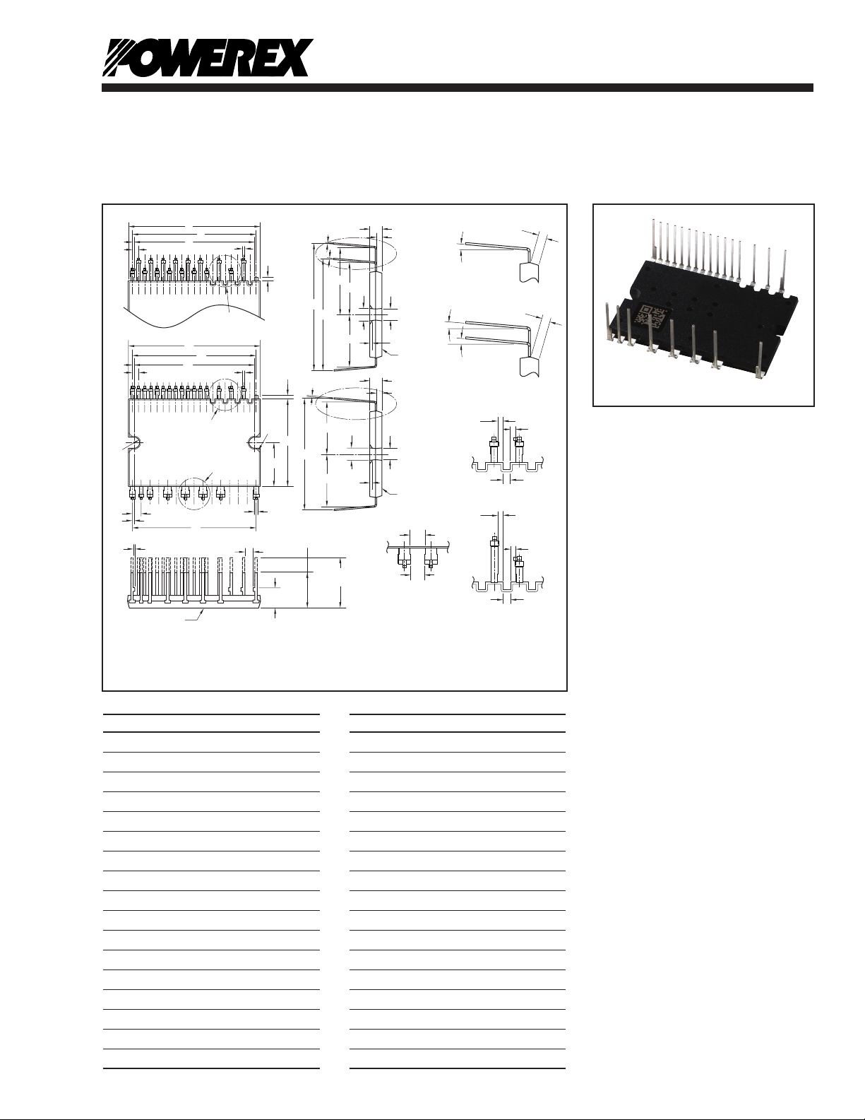
Outline Drawing and Circuit Diagram
Dimensions Inches Millimeters
A 1.50±0.02 38.0±0.5
B 0.94±0.02 24.0±0.5
C 0.14 3.5
D 1.40 35.56
E 0.57±0.02 14.4±0.5
F 0.74±0.02 18.9±0.5
G 1.15±0.02 29.2±0.5
H 0.14 3.5
J 0.13 3.3
K 0.016 0.4
L 0.06±0.02 1.5±0.05
M 0.031 0.8
N 1.39±0.019 35.0±0.3
O 0.07±0.008 1.778±0.2
P 0.02 0.5
Q 0.47 12.0
R 0.011 0.28
Dimensions Inches Millimeters
S 0.12 2.8
T 0.024 0.6
U 0.1±0.008 2.54±0.2
V 1.33±0.02 33.7±0.5
W 0.03 0.678
X 0.04 1.0
Y 0.05 1.2
Z 1.40 35.56
AA 0.55±0.02 14.0±0.5
AB 0.37±0.02 9.5±0.5
AC 0.22±0.02 5.5±0.5
AD 0 ~ 5° 0 ~ 5°
AE 0.06 Min. 1.5 Min.
AF 0.05 1.2
AG 0.063 Rad. 1.6 Rad.
AH 0.118 Min. 3.0 Min.
AJ 0.098 Min. 2.5 Min.
Features:
£ Compact Packages
£ Single Power Supply
£ Integrated HVICs
£ Direct Connection to CPU
£ Reduced R
th
Applications:
£ Refrigerators
£ Air Conditioners
£ Small Servo Motors
£ Small Motor Control
Ordering Information:
PS21965-4 is a 600V, 20 Ampere
short pin DIP Intelligent Power
Module.
PS21965-4A – long pin type
PS21965-4C – zigzag pin type
1Rev. 03/07
Powerex, Inc., 173 Pavilion Lane, Youngwood, Pennsylvania 15697-1800 (724) 925-7272
FWDi
CHIP
POWER TERMINALS
CONTROL TERMINALS
IGBT
CHIP
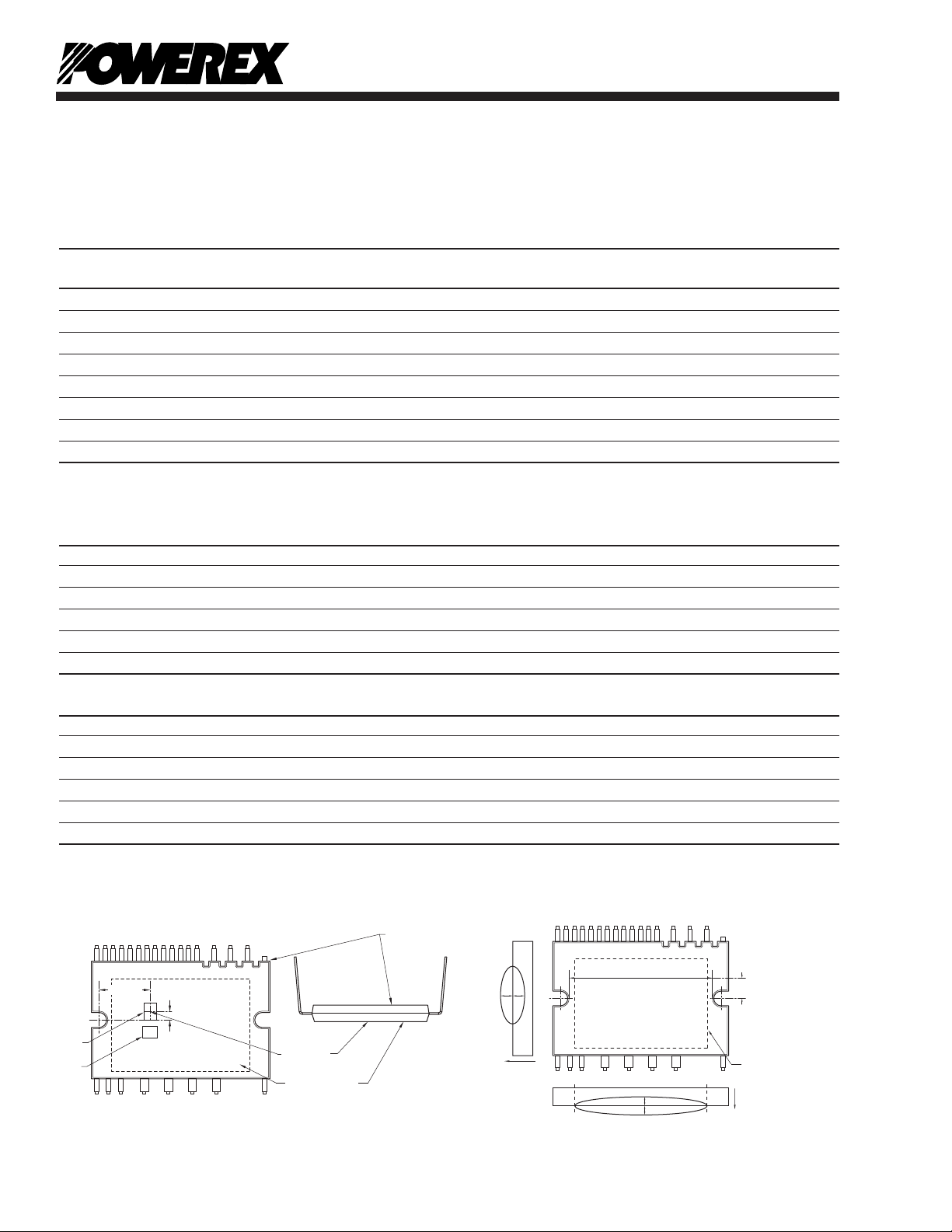
HEATSINK SIDE
TC POINT
11.6mm
3.0mm
DIP-IPM
HEATSINK
MEASUREMENT POINT
4.6mm
PLACE TO CONTACT
A HEATSINK
HEATSINK
–
+
–
+
PS21965-4, PS21965-4A, PS21965-4C
Intellimod™ Module
Dual-In-Line Intelligent Power Module
20 Amperes/600 Volts
Absolute Maximum Ratings, Tj = 25°C unless otherwise specified
PS21965-4, PS21965-4A
Characteristics Symbol PS21965-4C Units
Power Device Junction Temperature* Tj -20 to 150 °C
Storage Temperature T
-40 to 125 °C
stg
Case Operating Temperature (Note 1) TC -20 to 100 °C
Mounting Torque, M3 Mounting Screws — 6.9 in-lb
Module Weight (Typical) — 10 Grams
Heatsink Flatness (Note 2) — -50 to 100 µm
Self-protection Supply Voltage Limit (Short Circuit Protection Capability)** V
Isolation Voltage, AC 1 minute, 60Hz Sinusoidal, Connection Pins to Heatsink Plate V
*The ma ximum junction temperature rating of the power chips integrated within the DIP-IPM is 150°C (@TC ≤ 100°C). However, to ensure safe operation of the DIP-IPM,
the average junction temperature should be limited to T
**VD = 13.5 ~ 16.5V, Inverter Part, Tj = 125°C, Non-repetitive, Less than 2µs
≤125°C (@TC ≤ 100°C).
j(avg)
400 Volts
CC(prot.)
1500 Volts
ISO
IGBT Inverter Sector
Collector-Emitter Voltage V
Each Collector Current, ± (TC = 25°C) IC 20 Amperes
Each Peak Collector Current, ± (TC = 25°C, Less than 1ms) ICP 40 Amperes
Supply Voltage (Applied between P - N) VCC 450 Volts
Supply Voltage, Surge (Applied between P - N) V
Collector Dissipation (TC = 25°C, per 1 Chip) PC 35.7 Watts
600 Volts
CES
CC(surge)
500 Volts
Control Sector
Supply Voltage (Applied between VP1-VNC, VN1-VNC) VD 20 Volts
Supply Voltage (Applied between V
Input Voltage (Applied between UP, VP, WP-VNC, UN, VN, WN-VNC) VIN -0.5 ~ VD+0.5 Volts
Fault Output Supply Voltage (Applied between FO-VNC) VFO -0.5 ~ VD+0.5 Volts
Fault Output Current (Sink Current at FO Terminal) IFO 1 mA
Current Sensing Input Voltage (Applied between CIN-VNC) VSC -0.5 ~ VD+0.5 Volts
Note 1 – TC Measure Point
UFB
-U, V
VFB
-V, V
-W) VDB 20 Volts
WFB
Note 2 – Flatness Measurement Position
2 Rev. 03/07

Powerex, Inc., 173 Pavilion Lane, Youngwood, Pennsylvania 15697-1800 (724) 925-7272
PS21965-4, PS21965-4A, PS21965-4C
Intellimod™ Module
Dual-In-Line Intelligent Power Module
20 Amperes/600 Volts
Electrical and Mechanical Characteristics, Tj = 25°C unless otherwise specified
Characteristics Symbol Test Conditions Min. Typ. Max. Units
IGBT Inverter Sector
Collector-Emitter Saturation Voltage V
VD = VDB = 15V, IC = 20A, VIN = 5V, Tj = 125°C — 1.80 2.30 Volts
Diode Forward Voltage VEC -IC = 20A, VIN = 0V — 1.90 2.40 Volts
Inductive Load Switching Times ton 0.70 1.30 1.90 µs
trr VCC = 300V, VD = VDB = 15V, — 0.30 — µs
t
t
t
Collector Cutoff Current I
VCE = V
VD = VDB = 15V, IC = 20A, VIN = 5V, Tj = 25°C — 1.70 2.20 Volts
CE(sat)
IC = 20A, Tj = 125°C, — 0.50 0.75 µs
C(on)
VIN = 0 ⇔ 5V, Inductive Load, — 1.60 2.20 µs
off
C(off)
VCE = V
CES
— 0.40 0.75 µs
, Tj = 25°C — — 1.0 mA
CES
, Tj = 125°C — — 10 mA
CES
Control Sector
Circuit Current I
D VIN
VD = VDB = 15V V
VIN = 0V Total of VP1-VNC, VN1-VNC — — 2.80 mA
V
Fault Output Voltage V
V
Input Current IIN VIN = 5V 0.70 1.00 1.50 mA
Short Circuit Trip Level* V
Supply Circuit Under-voltage UV
UV
UVDt Trip Level, Tj ≤ 125°C 10.3 — 12.5 Volts
UVDr Reset Level, Tj ≤ 125°C 10.8 — 13.0 Volts
Fault Output Pulse Width** tFO 20 — — µs
ON Threshold Voltage V
OFF Threshold Voltage V
ON/OFF Threshold Hysteresis Voltage V
* Short Circuit protection is functioning only for the low-arms. Please select the value of the external shunt resistor such that the SC trip level is less than 1.7 times the current rating.
**Fault signal is asserted only for a UV or SC condition on the low side. On a SC fault the FO duration will be 20µsec. On a UV condition the fault signal will be asserted as long as the
UV condition exists or for 20µsec, whichever is longer.
= 5V Total of VP1-VNC, VN1-VNC — — 2.80 mA
-U, V
UFB
-U, V
UFB
VSC = 0V, FO Terminal Pull-up to 5V by 10kΩ 4.9 — — Volts
FOH
VSC = 1V, IFO = 1mA — — 0.95 Volts
FOL
VD = 15V* 0.43 0.48 0.53 Volts
SC(ref)
Trip Level, Tj ≤ 125°C 10.0 — 12.0 Volts
DBt
Reset Level, Tj ≤ 125°C 10.5 — 12.5 Volts
DBr
Applied between — 2.1 2.6 Volts
th(on)
UP, VP, WP-V
th(off)
UN, VN, WN-VNC 0.35 0.65 — Volts
th(hys)
VFB
VFB
-V, V
-V, V
-W — — 0.55 mA
WFB
-W — — 0.55 mA
WFB
0.8 1.3 — Volts
NC,
3Rev. 03/07

Powerex, Inc., 173 Pavilion Lane, Youngwood, Pennsylvania 15697-1800 (724) 925-7272
PS21965-4, PS21965-4A, PS21965-4C
Intellimod™ Module
Dual-In-Line Intelligent Power Module
20 Amperes/600 Volts
Thermal Characteristics
Characteristic Symbol Condition Min. Typ. Max. Units
Junction to Case R
R
Inverter IGBT (Per 1/6 Module) — — 2.8 °C/Watt
th(j-c)Q
Inverter FWDi (Per 1/6 Module) — — 3.9 °C/Watt
th(j-c)D
Recommended Conditions for Use
Characteristic Symbol Condition Min. Typ. Max. Units
Supply Voltage VCC Applied between P-N Terminals 0 300 400 Volts
Control Supply Voltage VD Applied between VP1-VNC, VN1-VNC 13.5 15.0 16.5 Volts
VDB Applied between V
V
Control Supply Variation
Arm Shoot-through Blocking Time t
Allowable Minimum Input P
Pulse Width* P
dVD, dVDB -1 — 1 V/µs
For Each Input Signal, TC ≤ 100°C 1.5 — — µs
DEAD
WIN(on)
0.5 — — µs
WIN(off)
VFB
-V, V
WFB
VNC Voltage Variation VNC Between VNC-N (Including Surge) -5.0 — 5.0 Volts
*DIP-IPM might not make response or work properly if the input signal plus width is less than the recommended minimum value.
UFB
-U,
13.0 15.0 18.5 Volts
-W
0.5 — — µs
4 Rev. 03/07

Powerex, Inc., 173 Pavilion Lane, Youngwood, Pennsylvania 15697-1800 (724) 925-7272
PS21965-4, PS21965-4A, PS21965-4C
Intellimod™ Module
Dual-In-Line Intelligent Power Module
20 Amperes/600 Volts
Application Circuit
5Rev. 03/07
Powerex, Inc., 173 Pavilion Lane, Youngwood, Pennsylvania 15697-1800 (724) 925-7272
A1
A4
A5
A2
SC
A7
A3
SET RESET
CR CIRCUIT TIME CONTAINS
DELAY (NOTE)
SC REFERENCE VOLTAGE
A6
A8
LOWER-ARMS
CONTROL INPUT
PROTECTION
CIRCUIT STATE
INTERNAL IGBT GATE
OUTPUT CURRENT I
C
SENSE VOLTAGE OF
THE SHU NT RESI STOR
FAULT OUTPUT F
O
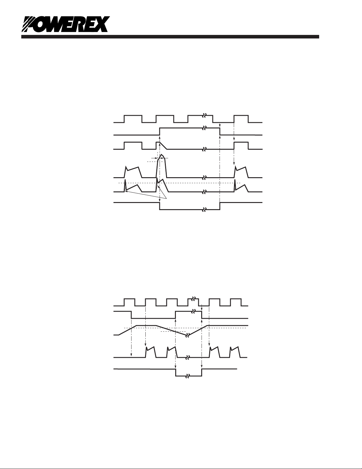
Short-Circuit Protection (Lower-arms only with the external shunt resistor and RC filter)
B1
B4
B5
B2
UV
Dt
B7
B3
SET
RESETRESET
UV
Dr
B6
CONTROL INPUT
PROTECT ION
CIRCU IT STATE
CONTR OL SUPPLY
VOLTAGE V
D
OUTPUT CURRENT I
C
FAULT OUTPUT F
O
Under-Voltage Protection (Lower-side, UVD)
A1: Normal operation – IGBT tur n on and conducting current.
A2: Short-circuit current detected (SC trigger).
A3: IGBT gate hard interrupted.
A4: IGBT tur n off.
A5: FO output with a fixed pulse width of t
FO(min)
= 20µs.
A6: Input “L” – IGBT off.
A7: Input “H” – IGBT on is blocked during the FO output period.
A8: IGBT stays in off state.
B1: Control supply voltage rise – After the voltage level reaches UVDr, the drive circuit begins to work
at the rising edge of the next input signal.
B2 : Normal operation – IGBT turn on and conducting current.
B3: Under-voltage trip (UVDt).
B4: IGBT turn off regardless of the control input level.
B5: FO output during under-voltage period, however, the minimum pulse width is 20µs.
B6: Under-voltage reset (UVDr).
B7: Normal operation – IGBT turn on and conducting current.
PS21965-4, PS21965-4A, PS21965-4C
Intellimod™ Module
Dual-In-Line Intelligent Power Module
20 Amperes/600 Volts
Protection Function Timing Diagrams
6 Rev. 03/07

Powerex, Inc., 173 Pavilion Lane, Youngwood, Pennsylvania 15697-1800 (724) 925-7272
C1
C4
C5
C2
UV
Dt
C6
C3
SET
RESETRESET
HIGH LEVEL (NO FAULT OUTPUT)
UV
DBr
CONTROL INPUT
PROTECTION
CIRCUIT STATE
CONTROL SUPPLY
VOLTAGE V
DB
OUTPUT CURRENT I
C
FAULT OUTPUT F
O
Under-Voltage Protection (Upper-side, UVDB)
C1: Control supply voltage rises – After the voltage level reaches UV
DBr
, the drive circuit begins to work
at the rising edge of the next input signal.
C2: Normal operation – IGBT turn on and conducting current.
C3: Under-voltage trip (UV
DBt
).
C4: IGBT stays off regardless of the control input level, but there is no FO signal output.
C5: Under-voltage reset (UVDr).
C6: Normal operation – IGBT turn on and conducting current.
V
NC
N
DIP-IPM
Wiring inductance should be less than 10nH.
(Equivalent to the inductance of a copper pattern with
length = 17mm, width = 3mm, and thickness = 100um.)
R
SHUNT
(Chip type resistor is recommended.)
This GND wiring from VNC should be as
close to the shunt resistors as possible.
UP, VP, WP, UN, VN, W
N
MCU
5V LINE
10kΩ
3.3kΩ (MIN)
F
O
VNC (LOGIC)
DIP-IPM
NOTE: RC coupling at each input
(parts shown dotted) may change
depending on the PWM control
scheme used in the application and
the wiring impedance of the printed
circuit board. The DIP-IPM input
signal section integrates a 3.3kΩ
(min) pull-down resistor. Therefore,
when using an external filtering
resistor, care must be taken to
satisfy the turn-on threshold voltage
requirement.
PS21965-4, PS21965-4A, PS21965-4C
Intellimod™ Module
Dual-In-Line Intelligent Power Module
20 Amperes/600 Volts
Protection Function Timing Diagrams
Typical Interface Circuit
Wiring Method Around Shunt Resistor
7Rev. 03/07
Powerex, Inc., 173 Pavilion Lane, Youngwood, Pennsylvania 15697-1800 (724) 925-7272
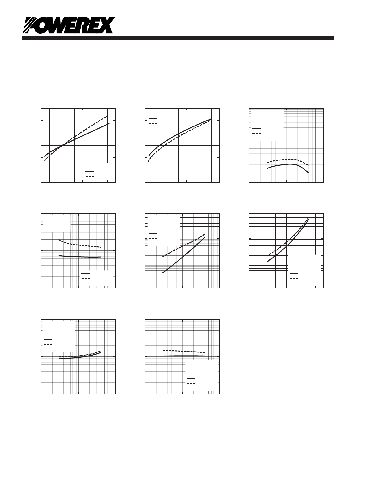
COLLECTOR CURRENT, IC, (AMPERES)
REVERSE RECOVERY CURRENT, I
rr
, (AMPERES)
REVERSE RECOVERY TIME, t
rr
, (ns)
10
0
10
2
10
1
10
0
10
2
10
1
COLLECTOR CURRENT, IC, (AMPERES)
REVERSE RECOVERY
CHARACTERISTICS (TYPICAL)
COLLECTOR-CURRENT, IC, (AMPERES)
EMITTER-COLLECTOR VOLTAGE, V
EC
, (VOLTS)
FREE-WHEEL DIODE
FORWARD CHARACTERISTICS
(TYPICAL)
REVERSE RECOVERY
CHARACTERISTICS (TYPICAL)
10
3
10
2
10
1
10
2
10
1
10
0
VD = 15V
Tj = 25°C
Tj = 125°C
VCC = 300V
V
CIN
= 0 ⇔ 5V
VD = 15V
Tj = 25°C
Tj = 125°C
INDUCTIVE LOAD
Tj = 25°C
Tj = 125°C
INDUCTIVE LOAD
VCC = 300V
V
CIN
= 0 ⇔ 5V
VD = 15V
COLLECTOR-EMITTER
SATURATION VOLTAGE, V
CE(sat)
, (VOLTS)
COLLECTOR-EMITTER
SATURATION VOLTAGE CHARACTERISTICS
(TYPICAL)
2.5
0.5
0
1.5
3.0
2.0
1.0
2.5
0.5
0
1.5
3.0
2.0
1.0
0 45403525 30105 15 20 0 45403525 30105 15 20
COLLECTOR-CURRENT, IC, (AMPERES)
VD = 15V
Tj = 25°C
Tj = 125°C
10
0
10
2
10
1
10
2
COLLECTOR CURRENT, IC, (AMPERES)
SWITCHING TIME, t
on
, (ns)
SWITCHING TIME (ON) VS.
COLLECTOR CURRENT (TYPICAL)
10
3
10
4
10
0
10
2
10
1
10
2
COLLECTOR CURRENT, IC, (AMPERES)
SWITCHING TIME, t
off
, (ns)
SWITCHING TIME (OFF) VS.
COLLECTOR CURRENT (TYPICAL)
10
3
10
4
VCC = 300V
V
CIN
= 0 ⇔ 5V
VD = 15V
Tj = 25°C
Tj = 125°C
INDUCTIVE LOAD
VCC = 300V
V
CIN
= 0 ⇔ 5V
VD = 15V
Tj = 25°C
Tj = 125°C
INDUCTIVE LOAD
COLLECTOR CURRENT, IC, (AMPERES)
SWITCHING LOSS, P
SW(off)
, (mJ/PULSE)
10
2
10
1
SWITCHING LOSS (OFF) VS.
COLLECTOR CURRENT (TYPICAL)
10
1
10
-1
10
0
10
-2
10
1
10
-1
10
0
10
-2
10
0
COLLECTOR CURRENT, IC, (AMPERES)
SWITCHING LOSS, P
SW(on)
, (mJ/PULSE)
10
2
SWITCHING LOSS (ON) VS.
COLLECTOR CURRENT (TYPICAL)
10
0
10
1
VCC = 300V
V
CIN
= 0 ⇔ 5V
VD = VDB = 15V
Tj = 25°C
Tj = 125°C
INDUCTIVE LOAD
VCC = 300V
V
CIN
= 0 ⇔ 5V
VD = 15V
Tj = 25°C
Tj = 125°C
INDUCTIVE LOAD
PS21965-4, PS21965-4A, PS21965-4C
Intellimod™ Module
Dual-In-Line Intelligent Power Module
20 Amperes/600 Volts
8 Rev. 03/07
 Loading...