

PS21342-G
Powerex, Inc., 200 Hillis Street, Youngwood, Pennsylvania 15697-1800 (724) 925-7272
A
D
R
C
HEATSINK
SIDE
35°
S
U
NC
NC
P
U
V
W
N
T
DUMMY
PINS
(5 PLACES)
G
J
B
AA DEEP
H
29
30
E
V
K
1314152122232425262728
FEE
F
3132333435
W
X
Y
Z
H
1324657981012 11161719 1820
M
N
AB
(2 PLACES)
L
Q
P
P
Q
TERMINAL CODE
15 V
1 V
2 NC
3 V
4 V
5 NC
6 U
7 V
UFS
UFB
P1
P
VFS
8 NC
9 V
10 V
11 NC
12 V
13 V
14 NC
WFB
16 V
17 NC
18 W
19 NC
20 NC
21 U
P1
P
N
VFB
P1
P
WFS
22 V
23 W
24 F
25 C
26 C
27 V
28 V
N
29
N
30
O
31
FO
32
33
IN
34
NC
35
N1
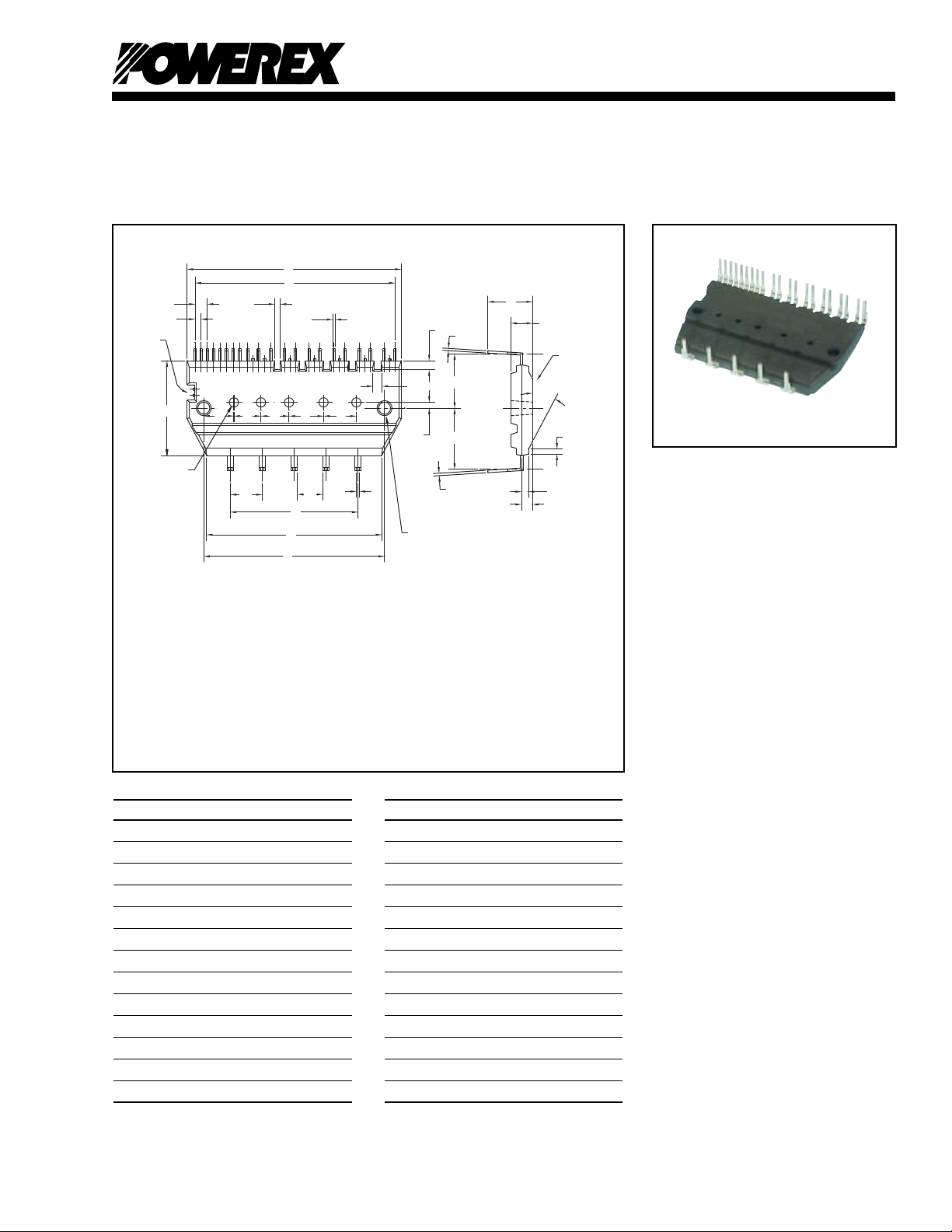
Intellimod™ Module
Dual-In-Line Intelligent
Power Module
5 Amperes/600 Volts
Description:
DIP and mini-DIP IPMs are
intelligent power modules that
integrate power devices, drivers,
and protection circuitry in an ultra
compact dual-in-line transfer-mold
package for use in driving small
three phase motors. Use of 4th
generation IGBTs, DIP packaging,
and application specific HVICs
allow the designer to reduce
inverter size and overall design
time.
Outline Drawing and Circuit Diagram
Dimensions Inches Millimeters
A 1.93 49.0
B 1.20 30.5
C 0.20 5.0
D 1.82 46.23
E 0.25 6.25
F 0.32 8.0
G 0.14 3.556
H 0.04 1.0
J 0.07 1.778
K 0.02 0.5
L 0.06 1.5
M 0.07 Min. 1.8 Min.
N 0.30 0.75
Dimensions Inches Millimeters
P 0.69 17.4
Q 0.02 0.5
R 0.41 10.5
S 0.05 1.2
T 0.05 1.25
U 0.10 2.5
V 0.30 7.62
W 0.16 Min. 4.0 Min.
X 1.20 30.48
Y 1.61 41.0
Z 1.65 42.0
AA 0.08 Dia. 2.0 Dia.
AB 0.13 Dia. 3.3 Dia.
Features:
□ Compact Packages
□ Single Power Supply
□ Integrated HVICs
□ Direct Connection to CPU
□ Optimized for 5kHz Operation
Applications:
□ Washing Machines
□ Refrigerators
□ Air Conditioners
□ Small Servo Motors
□ Small Motor Control
Ordering Information:
PS21342-G is a 600V, 5 Ampere
Mini-DIP Intelligent Power
Module.
115

Powerex, Inc., 200 Hillis Street, Youngwood, Pennsylvania 15697-1800 (724) 925-7272
PS21342-G
Intellimod™ Module
Dual-In-Line Intelligent Power Module
5 Amperes/600 Volts
Absolute Maximum Ratings, Tj = 25°C unless otherwise specified
Characteristics Symbol PS21342-G Units
Power Device Junction Temperature* T
Storage Temperature T
Heatsink T emperature (See Tf Measure Point Illustration) T
j
stg
f
-20 to 150 °C
-40 to 125 °C
-20 to 100 °C
Mounting Torque, M3 Mounting Screws — 8.5 in-lb
Module Weight (T ypical) — 20 Grams
Heatsink Flatness — -50 to 100 µm
Self-protection Supply Voltage Limit (Short Circuit Protection Capability)** V
Isolation Voltage, AC 1 minute, 60Hz Sinusoidal, Connection Pins to Heatsink Plate V
*The maximum junction temperature rating of the power chips integrated within the DIP-IPM is 150°C (@Tf ≤ 100°C). However, to ensure safe operation of the DIP-IPM,
the average junction temperature should be limited to T
**VD = 13.5 ~ 16.5V, Inverter Part, Tj = 125°C, Non-repetitive, Less than 2µs
≤ 125°C (@Tf ≤ 100°C).
j(avg)
CC(prot.)
ISO
400 Volts
1500 Volts
IGBT Inverter Sector
Collector-Emitter Voltage V
Collector Current, ± (TC = 25°C) I
Peak Collector Current, ± (TC = 25°C, Instantaneous Value (Pulse)) I
Supply Voltage (Applied between P - N) V
Supply Voltage, Surge (Applied between P - N) V
CC(surge)
Collector Dissipation (TC = 25°C, per 1 Chip) P
CES
C
CP
CC
C
600 Volts
5 Amperes
10 Amperes
450 Volts
500 Volts
20 Watts
Control Sector
Supply Voltage (Applied between VP1-VNC, VN1-VNC)V
Supply Voltage (Applied between V
UFB-VUFS, VVFB-VVFS
, V
WFB-VWFS
)VDB20 Volts
Input Voltage (Applied between UP, VP, WP-VNC, UN, VN, WN-VNC)V
Fault Output Supply Voltage (Applied between FO-VNC)V
Fault Output Current (Sink Current at FO Terminal) I
Current Sensing Input Voltage (Applied between CIN-VNC)V
D
CIN
FO
FO
SC
20 Volts
-0.5 ~ 5.5 Volts
-0.5 ~ VD+0.5 Volts
15 mA
-0.5 ~ VD+0.5 Volts
116

Powerex, Inc., 200 Hillis Street, Youngwood, Pennsylvania 15697-1800 (724) 925-7272
PS21342-G
Intellimod™ Module
Dual-In-Line Intelligent Power Module
5 Amperes/600 Volts
Electrical and Mechanical Characteristics, Tj = 25°C unless otherwise specified
Characteristics Symbol Test Conditions Min. Typ. Max. Units
IGBT Inverter Sector
Collector Cutoff Current I
Diode Forward Voltage V
Collector-Emitter Saturation Voltage V
Inductive Load Switching Times t
CES
EC
CE(sat)IC
IC = 5A, Tj = 125°C , VD = VDB = 15V, V
on
t
rr
t
C(on)
t
off
t
C(off)
= 5A, Tj = 25°C, VD = VDB = 15V, V
VCE = V
VCE = V
Tj = 25°C, -IC = 5A, V
, Tj = 25°C — — 1.0 mA
CES
, Tj = 125°C——10mA
CES
= 5V — 2.20 3.00 Volts
CIN
= 0V — 1.55 2.15 Volts
CIN
= 0V — 1.65 2.25 Volts
CIN
VCC = 300V, VD = 15V, 0.10 0.60 1.10 µS
IC = 5A, — 0.10 — µS
Tj = 125°C, — 0.20 0.60 µS
Inductive Load (Upper-Lower Arm), — 1.20 2.50 µS
V
= 5V(off), 0V(on) — 0.70 1.60 µS
CIN
Tf Measure Point
18 mm
FWDi CHIP
CONTROL TERMINALS
16 mm
NWV UP
POWER
TERMINALS
IGBT CHIP
Al BOARD
GROOVE
Tf MEASURE
POINT
(INSIDE THE
Al BOARD)
117

Powerex, Inc., 200 Hillis Street, Youngwood, Pennsylvania 15697-1800 (724) 925-7272
PS21342-G
Intellimod™ Module
Dual-In-Line Intelligent Power Module
5 Amperes/600 Volts
Electrical and Mechanical Characteristics, Tj = 25°C unless otherwise specified
Characteristics Symbol Test Conditions Min. Typ. Max. Units
Control Sector
Supply Voltage V
Circuit Current I
Fault Output Voltage V
PWM Input Frequency f
Allowable Dead Time t
Short Circuit Trip Level* V
Supply Circuit Under-voltage UV
Fault Output Pulse Width** t
ON Threshold Voltage (H-side) V
OFF Threshold Voltage (H-side) V
ON Threshold Voltage (L-side) V
OFF Threshold Voltage (L-side) V
* Short Circuit protection operates only at the low-arms. Please select the value of the external shunt resistor such that the SC trip level is less than 8.5A.
**Fault signal is asserted when the low-arm short circuit or control supply under-voltage protective functions operate. The fault output pulse-width tFO depends on the capacitance value of
CFO according to the following approximate equation: CFO = (12.2 x 10⁻⁶) x tFO {F} .
V
FOH
V
FOL
V
FO(sat)
PWM
DEAD
SC(ref)
UV
UV
UV
FO
th(on)
th(off)
th(on)
th(off)
D
DB
D
DBt
DBr
Dt
Dr
Applied between VP1-VNC, VN1-V
Applied between V
V
VFB-VVFS
VD = 15V, V
Total of VP1-VNC, VN1-V
VD = 15V, V
Total of VP1-VNC, VN1-V
VD = 15V, V
V
UFB-VUFS
, V
VFB-VVFS
VD = 15V, V
V
UFB-VUFS
, V
VFB-VVFS
UFB-VUFS
, V
WFB-VWFS
= 5V, VDB = 15V, — 4.25 8.50 mA
CIN
NC
= 0V, VDB = 15V, — 4.95 9.70 mA
CIN
NC
= 5V, VDB = 15V, — 0.50 1.00 mA
CIN
, V
WFB-VWFS
= 0V, VDB = 15V, — 0.50 1.00 mA
CIN
, V
WFB-VWFS
NC
, 13.5 15.0 16.5 Volts
13.5 15.0 16.5 Volts
VSC = 0V, FO Circuit: 10k Ω to 5V Pull-up 4.9 ——Volts
VSC = 1V, FO Circuit: 10k Ω to 5V Pull-up — 0.8 1.2 Volts
VSC = 1V, IFO = 15mA 0.8 1.2 1.8 Volts
Tj ≤ 125°C, Tf ≤ 100°C — 5 — kHz
Relates to Corresponding Input Signal for 3 ——µS
Blocking Arm Shoot-through (Tf ≤ 100°C)
Tj = 25°C, VD = 15V* 0.45 0.5 0.55 Volts
Trip Level, Tj ≤ 125°C 10.0 — 12.0 Volts
Reset Level, Tj ≤ 125°C 10.5 — 12.5 Volts
Trip Level, Tj ≤ 125°C 10.3 — 12.5 Volts
Reset Level, Tj ≤ 125°C 10.8 — 13.0 Volts
CFO = 22nF 1.0 1.8 — mS
Applied between UP, VP, WP-V
NC
0.8 1.4 2.0 Volts
2.5 3.0 4.0 Volts
Applied between UN, VN, WN-V
NC
0.8 1.4 2.0 Volts
2.5 3.0 4.0 Volts
118

Powerex, Inc., 200 Hillis Street, Youngwood, Pennsylvania 15697-1800 (724) 925-7272
PS21342-G
Intellimod™ Module
Dual-In-Line Intelligent Power Module
5 Amperes/600 Volts
Thermal Characteristics
Characteristic Symbol Condition Min. Typ. Max. Units
Junction to Heatsink R
th(j-f)Q
R
th(j-f)D
Each IGBT ——6.0 °C/Watt
Each FWDi ——6.5 °C/Watt
Recommended Conditions for Use
Characteristic Symbol Condition Min. Typ. Value Units
Supply Voltage V
Control Supply Voltage V
CC
D
V
DB
Control Supply dv/dt dVD/dt, dVDB/dt -1 — 1V/µs
Input ON Voltage V
Input OFF Voltage V
PWM Input Frequency f
Arm Shoot-through Blocking Time t
CIN(on)
CIN(off)
PWM
DEAD
Applied between P-N Terminals 0 300 400 Volts
Applied between VP1-VNC, VN1-V
Applied between V
V
VFB-VVFS
UFB-VUFS
, V
WFB-VWFS
Applied between UP, VP, WP-V
Applied between UN, VN, WN-V
NC
, 13.5 15.0 16.5 Volts
NC
NC
13.5 15.0 16.5 Volts
0 ~ 0.65 Volts
4.0 ~ 5.5 Volts
Tj ≤ 125°C, Tf ≤ 100°C — 5 — kHz
For Each Input Signal 3 ——µS
119

Powerex, Inc., 200 Hillis Street, Youngwood, Pennsylvania 15697-1800 (724) 925-7272
PS21342-G
Intellimod™ Module
Dual-In-Line Intelligent Power Module
5 Amperes/600 Volts
Mini-DIP IPM Application Circuit (Shown Pins Up)
+15V
+5V
R
2
C
5
R
2
C
5
CONTROLLER
R
2
C
5
This symbol indicates
connection to ground plane.
C
1
1
1
3
R2 x 3
C5 x 3
+
C
1
D1R
C
1
D1R
C
1
D1R
C
2
V
UFS
C
2
V
+
+
+
C
UFB
V
C
C
C
SF
P1
2
C
2
2
C
2
2
R
3
C
4
V
V
V
V
WFS
WFB
VFS
VFB
C
C
V
V
R
+V
U
CC
P
V
P1
V
P
V
P1
W
P
NC
U
N
V
N
W
N
F
O
FO
IN
NC
N1
SF
HVIC
+V
CC
HVIC
+V
CC
HVIC
INPUT SIGNAL
CONDITIONING
FAULT
LOGIC
PROT.
+V
CC
INPUT
CONDITION
INPUT
CONDITION
INPUT
CONDITION
UV
LVIC
UV PROT.
GATE DRIVE
LEVEL SHIFT
UV PROT.
GATE DRIVE
LEVEL SHIFT
UV PROT.
GATE DRIVE
LEVEL SHIFT
GATE DRIVE
PROTECTION
OVER CURRENT
P
C7C
6
+
U
V
MOTOR
W
R
SHUNT
N
AC LINE
120
Component Selection:
Dsgn. Typ. Value
D
C
C
C
C
C
C
C
C
R
R
R
R
R
Notes:
1) To prevent input signal oscillations minimize wiring length to controller (~2cm). Additional RC filtering (C5 etc.) may be
required. If filtering is added be careful to maintain proper dead time. See application notes for details.
2) Internal HVIC provides high voltage level shifting allowing direct connection of all six driving signals to the controller.
3) FO output is an open collector type. This signal should be pulled high with 5.1k ohm resistor (R3).
4) C4 sets the fault output duration and lock-out time. C4 ≈ 12.2E-6 x tFO, 22nF gives ~1.8ms
5) Boot strap supply component values must be adjusted depending on the PWM frequency and technique.
6) Wiring length associated with R
7) RSF, CSF set over current protection trip time. Recommend time constant is 1.5us-2.0us. See application notes.
8) Local decoupling/high frequency filter capacitors must be connected as close as possible to the modules pins.
9) The length of the DC link wiring between C6, C7, the DIP’s P terminal and the shunt must be minimized to prevent
excessive transient voltages. In particular C7 should be mounted as close to the DIP as possible.
10) Use high quality, tight tolorance current sensing resistor. Connect resistor as close as possible to the DIP’s
N terminal. Be careful to check for proper power rating. See application notes for calculation of resistance value.
1A, 600V Boot strap supply diode – Ultra fast recovery
1
1-100uF, 50V Boot strap supply reservoir – Electrolytic, long life, low Impedance, 105°C (Note 5)
1
0.22-2.0uF, 50V Local decoupling/High frequency noise filters – Multilayer ceramic (Note 8)
2
10-100uF, 50V Control power supply filter – Electrolytic, long life, low Impedance, 105°C
3
22nF, 50V Fault lock-out timing capacitor – Multilayer ceramic (Note 4)
4
100-1000pF, 50V Input signal noise filter – Multilayer ceramic (Note 1)
5
200-2000uF, 450V Main DC bus filter capacitor – Electrolytic, long life, high ripple current, 105°C
6
0.1-0.22uF, 450V Surge voltage suppression capacitor – Polyester/Polypropylene film (Note 9)
7
1000pF, 50V Short circuit detection filter capacitor – Multilayer Ceramic (Note 6, Note 7)
SF
1.8k ohm Short circuit detection filter resistor (Note 6, Note 7)
SF
5-100mohm Current sensing resistor – Non-inductive, temperature stable, tight tolerance (Note 10)
SHUNT
1-100 ohm Boot strap supply inrush limiting resistor (Note 5)
1
4.7k ohm Control input pull-up resistor (Note 1, Note 2)
2
5.1k ohm Fault output signal pull-up resistor (Note 3)
3
Description
, RSF, CSF must be minimized to avoid improper operation of the OC function.
SHUNT
 Loading...