POWEREX PS11016 Datasheet

MITSUBISHI SEMICONDUCTOR <Application Specific Intelligent Power Module>
MITSUBISHI SEMICONDUCTOR <Application Specific Intelligent Power Module>
PS11016
FLAT-B ASE TYPE
FLA T -B ASE TYPE
INSULA TED TYPE
PS11016
PS11016
INSULA TED TYPE
INTEGRATED FUNCTIONS AND FEATURES
• 3-phase IGBT inverter bridge configured by the latest 3rd.
generation IGBT and diode technologies.
• Circuit for dynamic braking of motor regenerative energy.
• Inverter output current capability I
Type Name
PS11016
100% load
11.0A (rms)
O (Note 1):
150% over load
16.5A (rms), 1min
(Note 1) : The inverter output current is assumed to be sinu-
soidal and the peak current value of each of the
above loading cases is defined as : I
OP = IO × √2
INTEGRATED DRIVE, PROTECTION AND SYSTEM CONTROL FUNCTIONS:
• For P-Side IGBTs :Drive circuit, High voltage isolated high-speed level shifting, Short-circuit protection (SC),
• For N-Side IGBTs :Drive circuit, Short circuit protection (SC), Control-supply Under voltage and Over voltage protection (OV/UV), Sys-
• For Brake circuit IGBT : Drive circuit
• Warning and Fault signaling :
F
F
F
CL : Warning for inverter current o verload condition
• For system feedback control : Analogue signal feedback reproducing actual inverter phase current (3φ).
• Input Interface : 5V CMOS/TTL compatible, Schmitt trigger input, and Arm-Shoot-Through interlock protection.
Bootstrap circuit supply scheme (Single drive-power-supply) and Under voltage protection (UV).
tem Over-temperature protection (OT), Fault output (F
O) signaling circuit, and Current-Limit warning signal output
(CL)
O1 : Short circuit protection for lower-leg IGBTs and Input interlocking against spurious arm shoot-through.
O2 : N-side control supply abnormality locking (OV/UV)
O3 : System over-temperature protection (OT).
APPLICATION
Acoustic noise-less 2.2kW/AC200V class 3 phase inverter and other motor control applications.
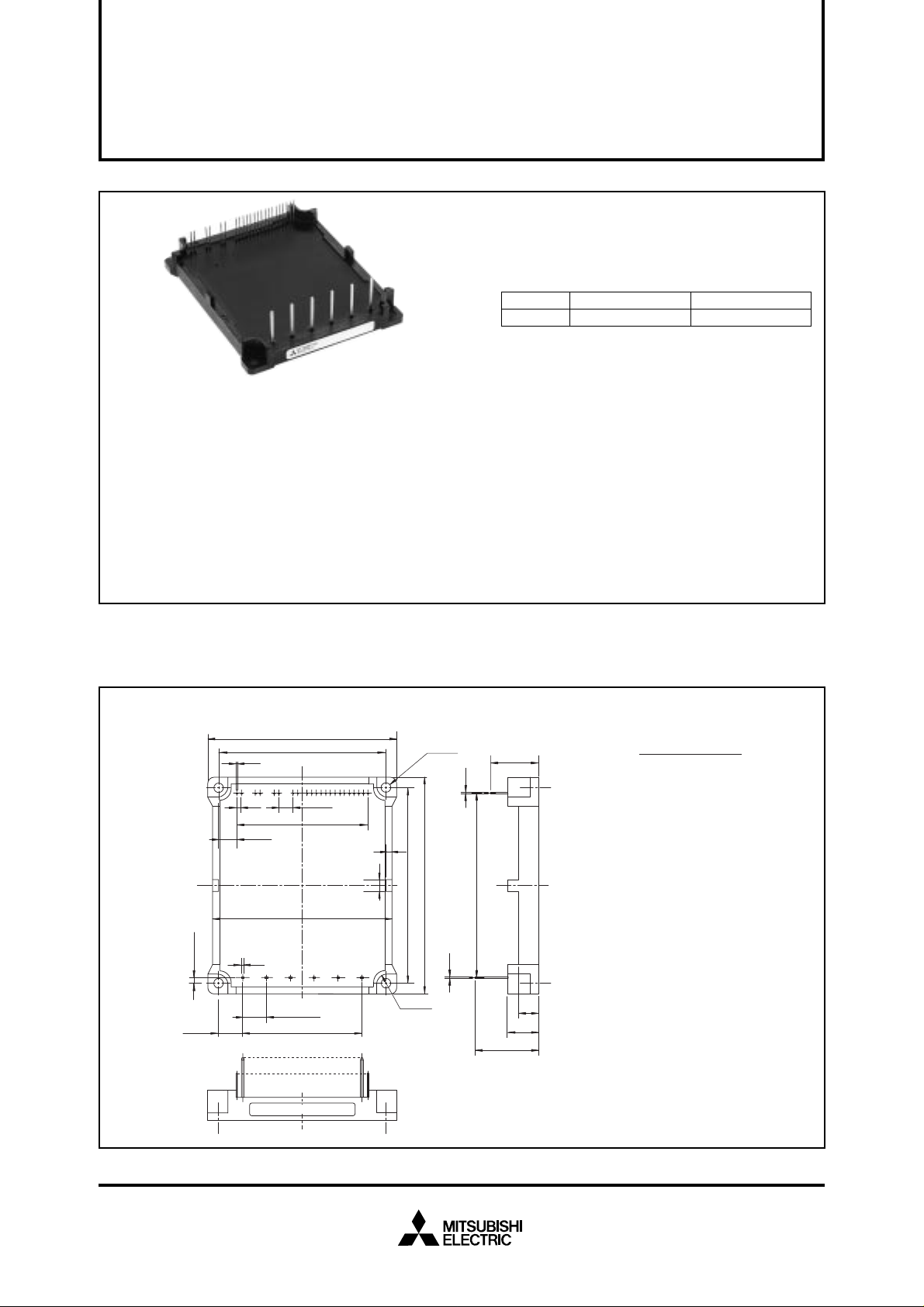
PACKAGE OUTLINES
80.5
± 1
71.5
± 0.3
2.45
(10.35)
10.16
50.8
± 0.5
6
± 0.3
56
± 0.8
76.5
± 1
33
± 0.3
± 0.8
0.5
± 0.3
2
(7.75)
1.2
31 32 34 35 36
4-φ4
231
2.5
5
± 1
± 0.5
92.5
83.5
0.6
4-R4
0.5
78.75
20.4
27
± 1
8.5
13
± 1
Terminals Assignment:
1 CBU+
2 CBU–
3 CBV+
4 CBV–
5 CBW+
6 CBW–
7 GND
8 NC
9 VDH
10 CL
11 FO1
12 FO2
13 FO3
14 CU
15 CV
16 CW
17 UP
18 VP
19 WP
20 UN
21 VN
22 WN
23 Br
31 P
32 Br
33 N
34 U
35 V
36 W
(Fig. 1)
LABEL
Jan. 2000

MITSUBISHI SEMICONDUCTOR <Application Specific Intelligent Power Module>
PS11016
FLAT-B ASE TYPE
INSULA TED TYPE
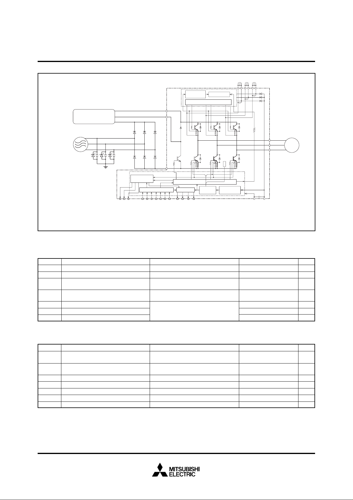
INTERNAL FUNCTIONS BLOCK DIAGRAM
Brake resistor connection,
Inrush prevention circuit,
etc.
AC 200V line input
Z : Surge absorber.
C : AC filter (Ceramic condenser 2.2~6.5nF)
[Note : Additionally an appropriate Line-to line
surge absorber circuit may become necessary
depending on the application environment].
Note 1) To prevent chances of signal oscillation, a series resistor (1kΩ) coupling at each output is recommended.
Note 2) By virtue of integrating an photo-coupler inside the module, direct coupling to CPU, without any external opto or transformer isolation is possible.
Note 3) All outputs are open collector type. Each signal line should be pulled up to plus side of the 5V power supply with approximately 5.1kΩ resistance.
Note 4) The wiring between power DC link capacitor and P/N terminals should be as short as possible to protect the ASIPM against catastrophic high surge voltage.
For extra precaution, a small film snubber capacitor (0.1~0.22µF, high voltage type) is recommended to be mounted close to these P and N DC power input pins.
R
S
T
CZ
Analogue signal output corresponding to
each phase current (5V line) Note 1)
CUCV CW
(Fig. 2)
MAXIMUM RATINGS (Tj = 25°C)
INVERTER PART (Including Brake Part)
V
CC
VCC(surge)
VP or VN
V
P(S)
±IC(±ICP)
C(ICP)
I
F(IFP)
I
Supply voltage
Supply voltage (surge)
Each output IGBT collector-emitter static voltage
Each output IGBT collector-emitter
or V
N(S)
switching surge voltage
Each output IGBT collector current
Brake IGBT collector current
Brake diode anode current
Current sensing
circuit
Input signal conditioning
UPVPWPVNWNB
PWM input
(5V line) Note 2)
Applied between P-N
Applied between P-N, Surge-value
Applied between P-U, V, W, Br or U, V, W,
Br-N
Applied between P-U, V, W, Br or U, V, W,
Br-N
T
Note: “( )” means I
P
B
N
U
N
C = 25°C
Application Specific Intelligent
Power Module
Protection
Circuit
Drive Circuit
Fo Logic
r
1
, FO2, FO
Fault output
(5V line) Note 3)
3
CL, FO
Level shifter
Drive Circuit
Protection
circuit
Control supply
T
S
fault sense
CBU–
CBU+
CBV–
CBV+
CBW–
CBW+
VDHGND
U
V
W
AC 200V line
output
ConditionSymbol Item Ratings Unit
450
500
600
600
±30 (±60)
C peak value
15 (30)
15 (30)
M
V
V
V
V
A
A
A
CONTROL PART
Symbol Item
VDH, VDB Supply voltage
CIN
V
VFO
IFO
VCL
ICL
ICO
Input signal voltage
Fault output supply voltage
Fault output current
Current-limit warning (CL) output voltage
CL output current
Analogue current signal output current
Condition
Applied between V
C
BV+-CBV–, CBW+-CBW–
Applied between U
W
N · Br-GND
Applied between F
Sink current of F
DH-GND, CBU+-CBU–,
P · VP · WP · UN · VN ·
O1 · FO2 · FO3-GND
O1 · FO2 · FO3
Applied between CL-GND
Sink current of CL
Sink current of CU · CV · CW
Ratings Unit
20
–0.5 ~ 7.5
–0.5 ~ 7
15
–0.5 ~ 7
15
±1
Jan. 2000
V
V
V
mA
V
mA
mA
 Loading...