POWEREX FX6KMJ-06 Datasheet

PRELIMINARY
Notice: This is not a final specification.
Some parametric limits are subject to change.
MITSUBISHI Pch POWER MOSFET
FX6KMJ-06
HIGH-SPEED SWITCHING USE
FX6KMJ-06
4V DRIVE
•
VDSS ...............................................................–60V
•
rDS (ON) (MAX) ................................................ 0.21Ω
•
ID ......................................................................–6A
•
Integrated Fast Recovery Diode (TYP.) ...........50ns
•
Viso ................................................................................2000V
•
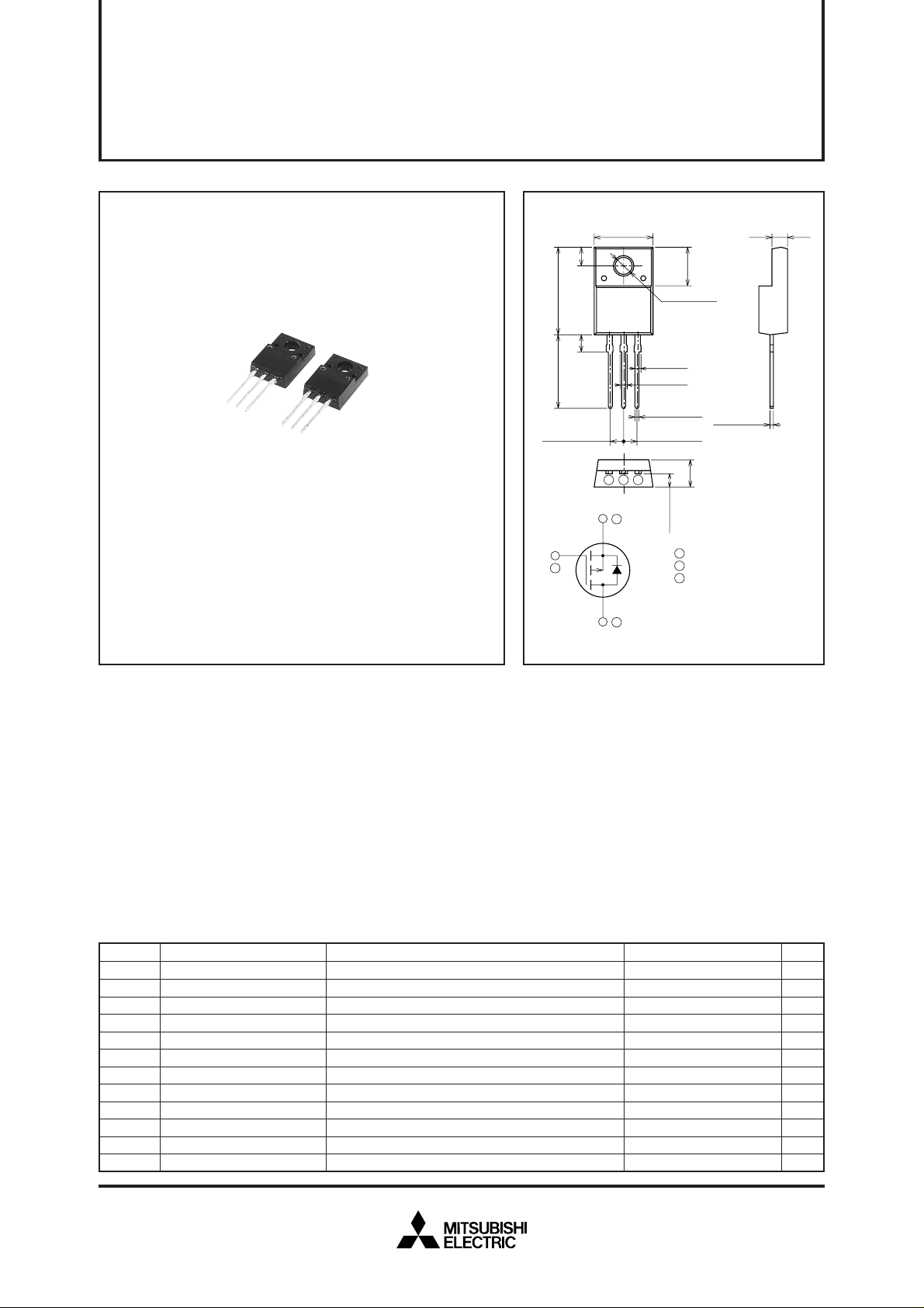
OUTLINE DRAWING Dimensions in mm
10 ± 0.3 2.8 ± 0.2
3 ± 0.33.6 ± 0.3
15 ± 0.314 ± 0.5
1
2
3
1
3
2
6.5 ± 0.3
φ 3.2 ± 0.2
1.1 ± 0.2
1.1 ± 0.2
0.75 ± 0.15
2.54 ± 0.252.54 ± 0.25
2.6 ± 0.2
1
2
3
E
0.75 ± 0.15
4.5 ± 0.2
GATE
DRAIN
SOURCE
TO-220FN
APPLICATION
Motor control, Lamp control, Solenoid control
DC-DC converter, etc.
MAXIMUM RATINGS (Tc = 25°C)
Symbol
VDSS
VGSS
ID
IDM
IDA
IS
ISM
PD
Tch
Tstg
Viso
—
Drain-source voltage
Gate-source voltage
Drain current
Drain current (Pulsed)
Avalanche drain current (Pulsed)
Source current
Source current (Pulsed)
Maximum power dissipation
Channel temperature
Storage temperature
Isolation voltage
Weight
Parameter Conditions Ratings Unit
VGS = 0V
VDS = 0V
L = 100µH
AC for 1minute, Terminal to case
Typical value
–60
±20
–6
–24
–6
–6
–24
20
–55 ~ +150
–55 ~ +150
2000
2.0
V
V
A
A
A
A
A
W
°C
°C
V
g
Jan.1999

PRELIMINARY
Notice: This is not a final specification.
Some parametric limits are subject to change.
ELECTRICAL CHARACTERISTICS (Tch = 25°C)
Symbol UnitParameter Test conditions
V
(BR) DSS
IGSS
IDSS
VGS (th)
rDS (ON)
rDS (ON)
VDS (ON)
yfs
Ciss
Coss
Crss
td (on)
tr
td (off)
tf
VSD
Rth (ch-c)
trr
Drain-source breakdown voltage
Gate-source leakage current
Drain-source leakage current
Gate-source threshold voltage
Drain-source on-state resistance
Drain-source on-state resistance
Drain-source on-state voltage
Forward transfer admittance
Input capacitance
Output capacitance
Reverse transfer capacitance
Turn-on delay time
Rise time
Turn-off delay time
Fall time
Source-drain voltage
Thermal resistance
Reverse recovery time
ID = –1mA, VGS = 0V
VGS = ±20V, VDS = 0V
VDS = –60V, VGS = 0V
ID = –1mA, VDS = –10V
ID = –3A, VGS = –10V
ID = –3A, VGS = –4V
ID = –3A, VGS = –10V
ID = –3A, VDS = –5V
VDS = –10V, VGS = 0V, f = 1MHz
VDD = –30V, ID = –3A, VGS = –10V, RGEN = RGS = 50Ω
IS = –3A, VGS = 0V
Channel to case
IS = –6A, dis/dt = 100A/µs
MITSUBISHI Pch POWER MOSFET
FX6KMJ-06
HIGH-SPEED SWITCHING USE
Limits
Min. Typ. Max.
–60
—
—
–1.3
—
—
—
—
—
—
—
—
—
—
—
—
—
—
—
—
—
–1.8
0.16
0.27
–0.48
4.9
1040
171
68
13
10
63
31
–1.0
—
50
—
±0.1
–0.1
–2.3
0.21
0.37
–0.63
—
—
—
—
—
—
—
—
–1.5
6.25
—
V
µA
mA
V
Ω
Ω
V
S
pF
pF
pF
ns
ns
ns
ns
V
°C/W
ns
PERFORMANCE CURVES
POWER DISSIPATION DERATING CURVE
40
32
24
16
8
POWER DISSIPATION PD (W)
0
0 20050 100 150
CASE TEMPERATURE T
OUTPUT CHARACTERISTICS
–20
PD = 20W
–16
Tc = 25°C
Pulse Test
–12
(TYPICAL)
VGS = –10V
–8V
C (°C)
–6V
–5V
MAXIMUM SAFE OPERATING AREA
–5
–3
–2
2
–10
–7
–5
–3
–2
1
–10
DRAIN CURRENT ID (A)
–10
–7
–5
–3
–2
0
–7
–5
TC = 25°C
Single Pulse
–2 –10
–3 –5–7 –2 –10
0
–3 –5–7 –2
DRAIN-SOURCE VOLTAGE V
OUTPUT CHARACTERISTICS
(TYPICAL)
–10
–8
Tc = 25°C
Pulse Test
VGS = –10V
–6
1
tw =
–3 –5–7
–8V
–6V
10µs
100µs
1ms
10ms
DC
–10
DS (V)
–5V
–4V
2
–2
–8
–4
DRAIN CURRENT ID (A)
0
0 –1.0 –2.0 –3.0 –4.0 –5.0
DRAIN-SOURCE VOLTAGE VDS (V)
–4V
–3V
–4
–2
DRAIN CURRENT ID (A)
0
0 –0.4 –0.8 –1.2 –1.6 –2.0
DRAIN-SOURCE VOLTAGE VDS (V)
–3V
Jan.1999
 Loading...