

MITSUBISHI HVIGBT MODULES
CM800DZ-34H
3rd-Version HVIGBT (High Voltage Insulated Gate Bipolar Transistor) Modules
INSULATED TYPE
CM800DZ-34H
● IC...................................................................800A
HIGH POWER SWITCHING USE
● V
CES ....................................................... 1700V
● Insulated T ype
● 2-elements in a pack
APPLICATION
Inverters, Converters, DC choppers, Induction heating, DC to DC converters.
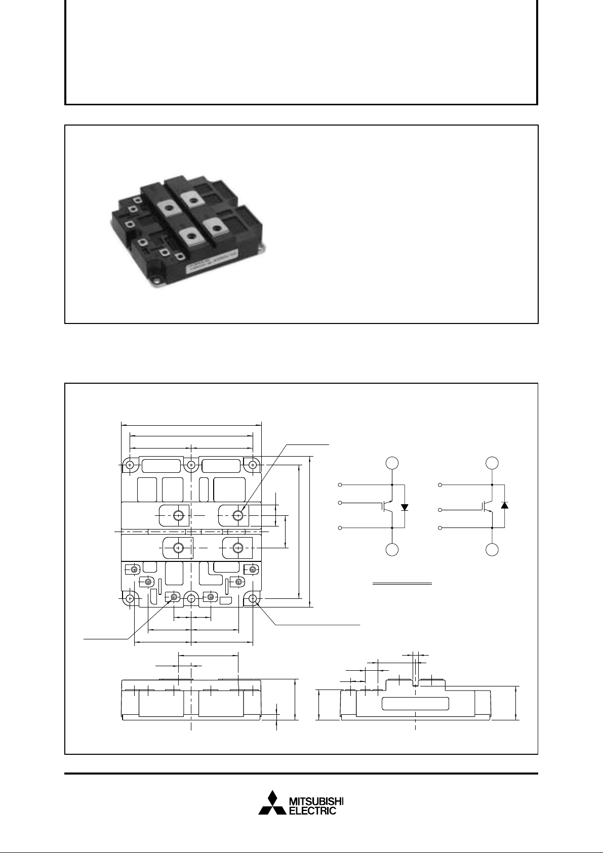
OUTLINE DRAWING & CIRCUIT DIAGRAM Dimensions in mm
130
6 - M4 NUTS
114
57±0.25 57±0.25
E1
C1
CM
E1 E2
C1
G1 G2
11.85
C2
E2
C2
16
18
4440
5753
55.2
4 - M8 NUTS
E1
20
±0.25
30
124
6 - φ 7 MOUNTING HOLES
140
G1
C1
14
11.5
E1
C1
CIRCUIT DIAGRAM
5
35
C2
C2
G2
E2
E2
38
5
HVIGBT MODULES (High Voltage Insulated Gate Bipolar Transistor Modules)
28
LABEL
31.5
Oct. 2002
MITSUBISHI HVIGBT MODULES
CM800DZ-34H
HIGH POWER SWITCHING USE
3rd-Version HVIGBT (High Voltage Insulated Gate Bipolar Transistor) Modules
MAXIMUM RATINGS (Tj = 25°C)
Symbol Item Conditions UnitRatings
VCES
VGES
IC
ICM
IE
IEM
PC
Tj
Tstg
Viso
Collector-emitter voltage
Gate-emitter voltage
Collector current
(Note 2)
Emitter current
(Note 2)
Maximum collector dissipation
(Note 3)
Junction temperature
Storage temperature
Isolation voltage
—
Mounting torque
—
Mass
VGE = 0V
CE = 0V
V
T
C = 25°C
Pulse (Note 1)
T
C = 25°C
Pulse (Note 1)
C = 25°C, IGBT part
T
—
—
Charged part to base plate, rms, sinusoidal, AC 60Hz 1min.
Main terminals screw M8
Mounting screw M6
Auxiliary terminals screw M4
Typical value
–40 ~ +150
–40 ~ +125
6.67 ~ 13.00
2.84 ~ 6.00
0.88 ~ 2.00
INSULATED TYPE
1700
±20
800
1600
800
1600
5000
4000
N·m
N·m
N·m
1.0
V
V
A
A
A
A
W
°C
°C
V
kg
ELECTRICAL CHARACTERISTICS (Tj = 25°C)
Symbol
I
CES
V
GE(th)
IGES
VCE(sat)
Cies
Coes
Cres
QG
td (on)
tr
td (off)
tf
VEC
trr
Qrr
Rth(j-c)Q
Rth(j-c)R
Rth(c-f)
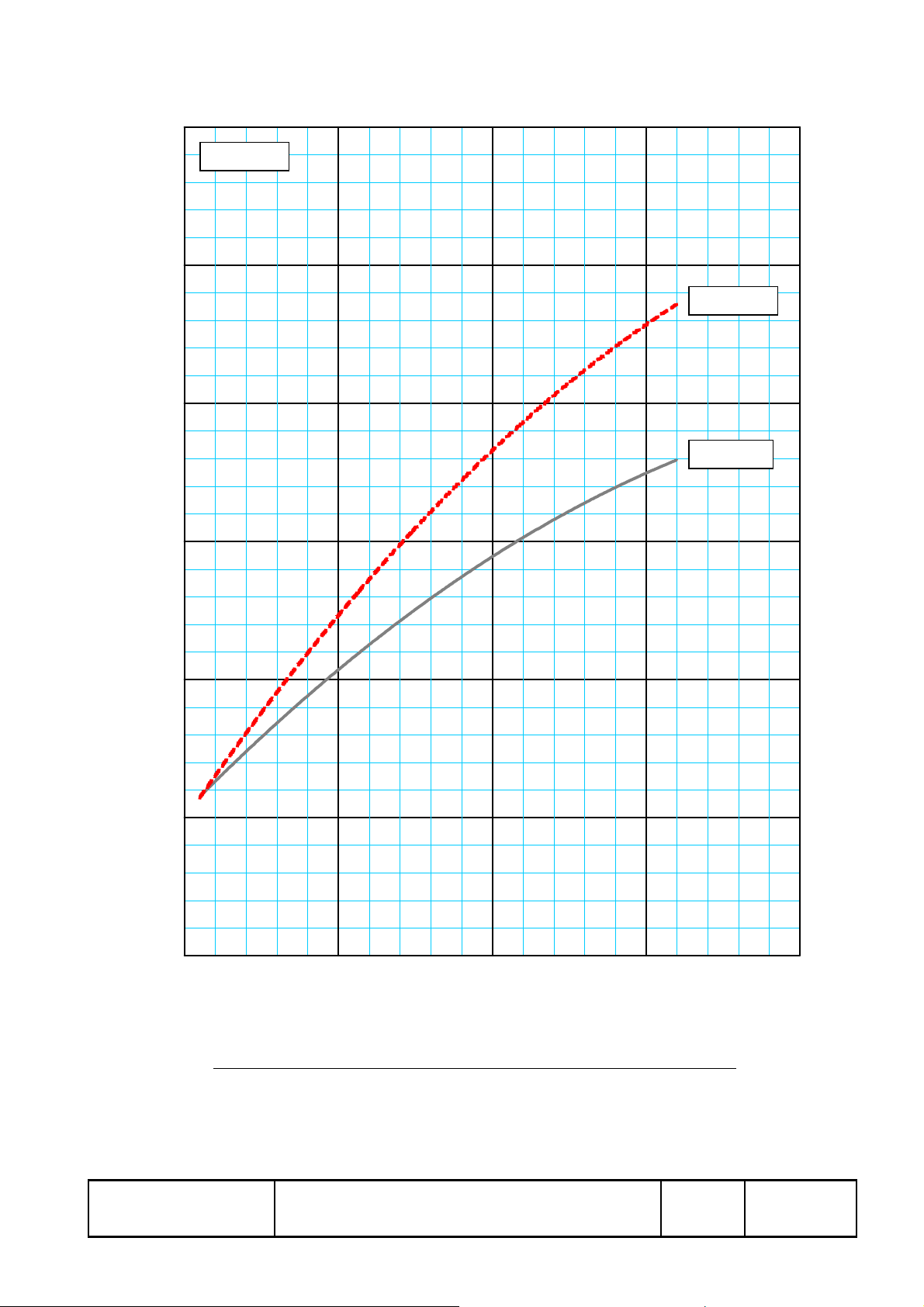
Note 1. Pulse width and repetition rate should be such that the device junction temp. (Tj) does not exceed Tjmax rating.
Collector cutoff current
Gate-emitter
threshold voltage
Gate-leakage current
Collector-emitter
saturation voltage
Input capacitance
Output capacitance
Reverse transfer capacitance
Total gate charge
Turn-on delay time
Turn-on rise time
Turn-off delay time
Turn-off fall time
(Note 2)
Emitter-collector voltage
(Note 2)
Reverse recovery time
(Note 2)
Reverse recovery charge
Thermal resistance
Contact thermal resistance
2. I
E, VEC, trr, Qrr & die/dt represent characteristics of the anti-parallel, emitter to collector free-wheel diode.
3. Junction temperature (T
4. Pulse width and repetition rate should be such as to cause negligible temperature rise.
Item Conditions
V
CE = VCES, VGE = 0V
IC = 80mA, VCE = 10V
V
GE = VGES, VCE = 0V
T
j = 25°C
j = 125°C
T
CE = 10V
V
V
GE = 0V
CC = 850V, IC = 800A, VGE = 15V
V
V
CC = 850V, IC = 800A
V
GE1 = VGE2 = 15V
R
G = 3.3Ω
I
C = 800A, VGE = 15V (Note 4)
Resistive load switching operation
I
E = 800A, VGE = 0V
I
E = 800A
die / dt = –1600A / µs
Junction to case, IGBT part (Per 1/2 module)
Junction to case, FWDi part (Per 1/2 module)
Case to fin, conductive grease applied (Per 1/2 module)
j) should not increase beyond 150°C.
Min Typ Max
Limits
—
—
5.54.5 6.5
—
—
—
—
—
—
—
—
—
—
—
—
—
—
—
—
—
—
2.80
3.20
72
9.0
3.6
6.6
—
—
—
—
2.60
—
150
—
—
0.020
0.025
0.043
12
0.5
3.64
—
—
—
—
—
1.60
2.00
2.70
0.80
3.38
2.70
—
—
Unit
mA
V
µA
V
nF
nF
nF
µC
µs
µs
µs
µs
V
µs
µC
K/W
K/W
K/W
HVIGBT MODULES (High Voltage Insulated Gate Bipolar Transistor Modules)
Oct. 2002

SECURITY
CODE
SPEC.NAME
Application
Note
Prepared by S.Iura S.Iura
Checked by M.Yamamoto I.Umesaki
Approved by M.Yamamoto M.Tabata
DATE Apr.8.2002
MITSUBISHI ELECTRIC CORPORATION
A
R
E
V
Aug.2.2002
Data Sheet
(CM800DZ−34H)
1. Output characteristics Page 2
2. Transfer characteristics Page 3
3. Collector-emitter saturation voltage characteristics Page 4 / 5
4. Free wheel diode forward characteristics Page 6
5. Capacitance characteristics Page 7
6. Gate charge characteristics Page 8
7. Half-bridge Switching time characteristics Page 9
8. Half-bridge Switching energy characteristics Page 10
9. Reverse recovery characteristics Page 11
10. Transient thermal impedance characteristics Page 12
A
11. Turn-off switching safe operating area Page 13
12. Short circuit safe operating area Page 14
13. Reverse recovery safe operating area Page 15
HVIGBT
HVM-1005-A
(P2-OU)
PAGE
1 / 15
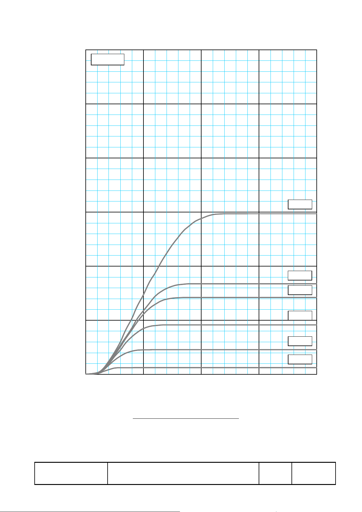
12000
Tj=25°C
10000
8000
6000
COLLECTOR CURRENT [A]
4000
2000
0
0 5 10 15 20
VGE=20V
VGE=15V
VGE=14V
VGE=12V
VGE=10V
VGE= 8V
HVIGBT
COLLECTOR-EMITTER VOLTAGE [V]
Output characteristics (typical)
HVM-1005-A
PAGE
(P2-OU)
2 / 15
12000
VCE=10V
10000
8000
6000
COLLECTOR CURRENT [A]
4000
2000
0
0 5 10 15 20
Tj=25°C
Tj=125°C
HVIGBT
GATE-EMITTER VOLTAGE [V]
Transfer characteristics (typical)
HVM-1005-A
PAGE
(P2-OU)
3 / 15
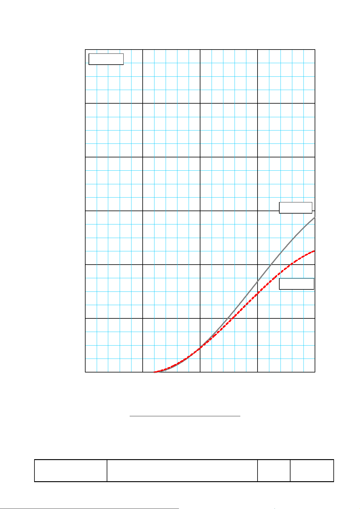
6
VGE=15V
5
Tj=125°C
4
Tj=25°C
3
2
COLLECTOR-EMITTER VOLTAGE [V]
1
0
0 500 1000 1500 2000
HVIGBT
COLLECTOR CURRENT [A]
Collector-emitter saturation voltage characteristics (typical)
HVM-1005-A
(P2-OU)
PAGE
4 / 15

10
Tj=25°C
9
8
7
6
5
4
3
COLLECTOR-EMITTER SATURATION VOLTAGE [V]
2
1
0
0 5 10 15 20
Ic = 1600A
Ic = 800A
Ic = 400A
HVIGBT
GATE-EMITTER VOLTAGE [V]
Collector-emitter saturation voltage characteristics (typical)
HVM-1005-A
(P2-OU)
PAGE
5 / 15

5
4
Tj=25°C
3
Tj=125°C
2
EMITTER-COLLECTOR VOLTAGE [V]
1
0
0 500 1000 1500 2000
HVIGBT
EMITTER CURRENT [A]
Free wheel diode forward voltage characteristics (typical)
HVM-1005-A
(P2-OU)
PAGE
6 / 15

1000
VGE=15V, Tj=25°C
: f=100kHz
C
ies
: f=100kHz
C
oes
: f=1MHz
C
res
100
CAPACITANCE [nF]
10
C
ies
C
oes
C
res
HVIGBT
1
0.1 1 10 100
COLLECTOR-EMITTER VOLTAGE [V]
Capacitance characteristics (typical)
PAGE
HVM-1005-A
(P2-OU)
7 / 15

20
VCC=850V
=800A
I
C
18
16
14
12
10
8
GATE-EMITTER VOLTAGE [V]
6
4
2
0
0 2500 5000 7500 10000
HVIGBT
GATE CHARGE [nC]
Gate charge characteristics (typical)
HVM-1005-A
(P2-OU)
PAGE
8 / 15

10
VCC=850V, VGE=±15V
=3.3Ω, Tj=125°C, LS=150nH
R
G
Inductive load
t
t
tr
d(off)
d(on)
1
s]
µ
SWITCHING TIME [
0.1
0.01
10 100 1000 10000
tf
COLLECTOR CURRENT [A]
HVIGBT
Half-bridge switching time characteristics (typical)
HVM-1005-A
(P2-OU)
PAGE
9 / 15

1.2
VCC=850V, VGE=±15V
=3.3Ω, Tj=125°C, LS=150nH
R
G
Inductive load
Integrated over range of 10%
1
0.8
0.6
SWITCHING ENERGY [J/P]
0.4
0.2
Eon
E
off
E
rec
0
HVIGBT
0 400 800 1200 1600
COLLECTOR / EMITTER CURRENT [A]
Half-bridge switching energy characteristics (typical)
HVM-1005-A
(P2-OU)
PAGE
10 / 15

s]
µ
100
10
VCC=850V, Tj=125°C
=150nH, Inductive load
L
S
IGBT drive conditions
=±15V, RG=3.3Ω
V
GE
10000
1000
Irr
trr
REVERSE RECOVERY TIME [
1
0.1
10 100 1000 10000
EMITTER CURRENT [A]
Reverse recovery characteristics (typical)
100
10
REVERSE RECOVERY CURRENT [A]
HVIGBT
HVM-1005-A
(P2-OU)
PAGE
11 / 15

j
=0.034 K/W
=0.020 K/W
-c)
th(
th(j-c)
: R
.
Single pulse
Tc = 25°C
IGBT part
FWDi part: R
TIME [second]
0.001 0.010 0.100 1.000 10.000
1.2
1.0
0.8
0.6
0.4
0.2
0.0
NORMALIZED TRANSIENT THERMAL IMPEDANCE
Transient thermal impedance characteristics
HVIGBT
HVM-1005-A
(P2-OU)
PAGE
12 / 15

3000
VCC≤1150V, VGE=±15V
≥3.3Ω, Tj=125°C
R
G
2500
2000
1500
COLLECTOR CURRENT [A]
1000
500
0
0 500 1000 1500 2000
HVIGBT
COLLECTOR-EMITTER VOLTAGE [V]
Turn-off switching safe operating area (SWSOA / RBSOA)
HVM-1005-A
(P2-OU)
PAGE
13 / 15

6000
VCC≤1150V, VGE=±15V
≥3.3Ω, Tj=125°C
R
G
tw≤10µs
5000
4000
3000
COLLECTOR CURRENT [A]
2000
1000
0
0 500 1000 1500 2000
HVIGBT
COLLECTOR-EMITTER VOLTAGE [V]
Short circuit safe operating area (SCSOA)
HVM-1005-A
(P2-OU)
PAGE
14 / 15

2500
VCC≤1150V, Tj=125°C
di/dt≤1800A/µs
2000
1500
1000
REVERSE RECOVERY CURRENT [A]
500
0
0 500 1000 1500 2000
EMITTER-COLLECTOR VOLTAGE [V]
Reverse recovery safe operating area (RRSOA / Di-SOA)
HVIGBT
HVM-1005-A
(P2-OU)
PAGE
15 / 15
 Loading...