

Page 1
CM75RX-34SA
Powerex, Inc., 173 Pavilion Lane, Youngwood, Pennsylvania 15697 (724) 925-7272
www.pwrx.com
AT
BE
AH
Q
C
P(21)
GuP(20)
EuP(19)
U(1)
GuN(18)
N(22)
AV
AU
DETAIL "B"
AM
BD
AA
P
M
N
E
DETAIL "B"
GvP(16)
EvP(15)
V(2) W(3)
GvN(14)
K
BB
BA
Y
K
W
V
AB (4 PLACES)
21
22
H
GwP(12)
EwP(11)
GwN(10)
EwN(9)EvN(13)EuN(17)
U
AF (6 PLACES)
1 2 3 4
X
B(4)
GB(6)
EB(5)
T
S
R
L
BB
Y
BB BB
Y
Y
A
D
F
G
DETAIL "C"
TH
TH1
2
(7)
(8)
NTC
BB
Y
DETAIL "A"
ZZZ
Tolerance Otherwise Specified (mm)
Division of Dimension Tolerance
0.5 to 3 ±0.2
over 3 to 6 ±0.3
over 6 to 30 ±0.5
over 30 to 120 ±0.8
over 120 to 400 ±1.2
The tolerance of size between
terminals is assumed to ±0.4
BC
BA
Y
10 912 1114 1316 1518 1720 19
8
7
6
5
AC
AD
AE
AR
AS
AP
DETAIL "A"
AW
AX
DETAIL "C"
Y
B
AQ
K
AE
AM
AZ
AY
Y
AL
AJ
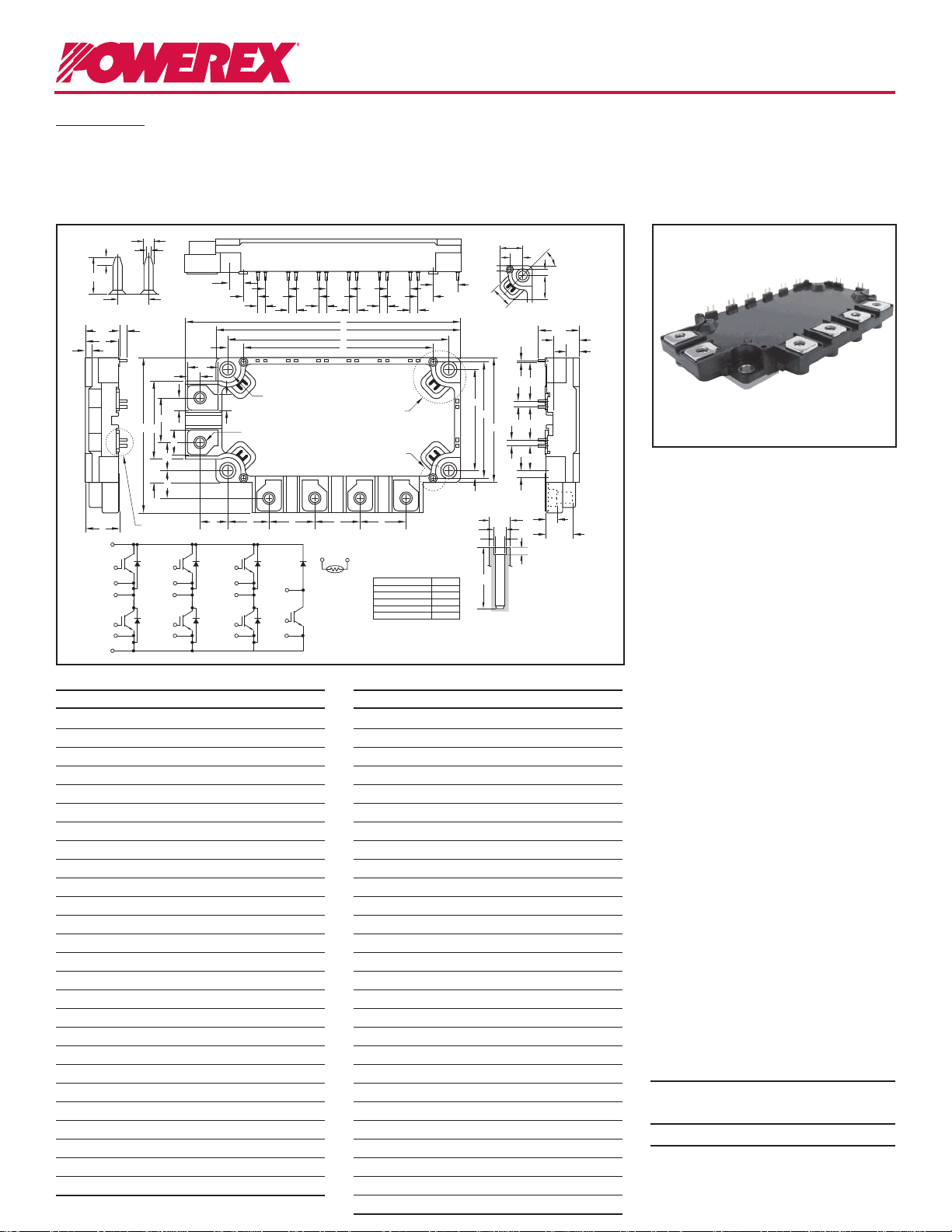
Outline Drawing and Circuit Diagram
Dimensions Inches Millimeters
A 5.39 136.9
B 2.44 62.0
C 0.67+0.04/-0.02 17.0+1.0/-0.5
D 4.79 121.7
E 0.45 11.5
F 4.33±0.02 110.0±0.5
G 3.72 94.5
H 0.53 13.5
J 0.23 5.9
K 0.30 7.75
L 0.53 13.64
M 3.02 77.1
N 1.53 39.0
P 0.87 22.0
Q 0.65 16.5
R 0.55 14.0
S 0.47 12.0
T 0.24 6.0
U 0.31 8.0
V 0.37 6.5
W 0.61 15.64
X 0.81 20.71
Y 0.15±0.008 3.81±0.2
Z 0.9 22.86
AA 0.14 3.5
AB 0.22 Dia. 5.5 Dia.
Dimensions Inches Millimeters
AC 1.97±0.02 50.0±0.5
AD 2.26 57.5
AE 0.14 3.75
AF M5 M5
AG 0.27 7.0
AH 0.67 17.0
AJ 0.44±0.008 11.67±0.2
AK 0.81 20.5
AL 0.60±0.008 15.24±0.2
AM 0.12 3.0
AN 0.53 13.4
AP 0.49 12.5
AQ 0.18 Dia. 4.5 Dia.
AR 0.102 Dia. 2.6 Dia.
AS 0.088 Dia. 2.25 Dia.
AT 0.05 1.2
AU 0.02 0.65
AV 0.04 1.15
AW 0.54 13.7
AX 0.51 13.0
AY 0.75 19.12
AZ 0.021±0.008 0.55±0.2
BA 0.28±0.008 7.24±0.2
BB 0.43±0.008 11.42±0.2
BC 0.46±0.008 11.8±0.2
BD 0.15 3.81
BE 0.18 4.5
AW
Six IGBT + Brake
NX-Series Module
75 Amperes/1700 Volts
45°
AE
AK
AX
AG
Description:
Powerex IGBT Modules are
J
AN
designed for use in switching
applications. Each module
consists of six IGBT Transistors in
a three phase bridge configuration
and a seventh IGBT with freewheel diode for dynamic braking.
All components and interconnects
are isolated from the heat sinking
baseplate, offering simplified
system assembly and thermal
management.
Features:
£ Low Drive Power
£ Low V
CE(sat)
£ Discrete Super-Fast Recovery
Free-Wheel Diode
£ Isolated Baseplate for Easy
Heat Sinking
Applications:
£ AC Motor Control
£ Motion/Servo Control
£ Photovoltaic/Fuel Cell
Ordering Information:
Example: Select the complete
module number you desire from
the table below -i.e.
CM75RX-34SA is a 1700V (V
CES
),
75 Ampere Six-IGBT + Brake
Power Module.
Type Current Rating
Amperes Volts (x 50)
CM 75 34
V
CES
102/14 Rev. 1
Page 2
Powerex, Inc., 173 Pavilion Lane, Youngwood, Pennsylvania 15697 (724) 925-7272 www.pwrx.com
CM75RX-34SA
Six IGBT + Brake NX-Series Module
75 Amperes/1700 Volts
Absolute Maximum Ratings, Tj = 25°C unless otherwise specied
Inverter Part IGBT/Diode
Characteristics Symbol Rating Units
Collector-Emitter Voltage (VGE = 0V) V
Gate-Emitter Voltage (VCE = 0V) V
Collector Current (DC, TC = 125°C)
*2,*4
IC 75 Amperes
Collector Current (Pulse, Repetitive)*3 I
Total Power Dissipation (TC = 25°C)
*2,*4
P
Emitter Current*2 I
Emitter Current (Pulse, Repetitive)*3 I
1700 Volts
CES
±20 Volts
GES
150 Amperes
CRM
830 Watts
tot
*1
75 Amperes
E
*1
150 Amperes
ERM
Brake Part IGBT/Diode
Characteristics Symbol Rating Units
Collector-Emitter Voltage (VGE = 0V) V
Gate-Emitter Voltage (VCE = 0V) V
Collector Current (DC, TC = 125°C)
*2,*4
IC 50 Amperes
Collector Current (Pulse, Repetitive)*3 I
Total Power Dissipation (TC = 25°C)
*2,*4
P
Repetitive Peak Reverse Voltage (VGE = 0V) V
Forward Current*2 I
Forward Current (Pulse, Repetitive)*3 I
1700 Volts
CES
±20 Volts
GES
100 Amperes
CRM
600 Watts
tot
1700 Volts
RRM
*1
50 Amperes
F
*1
100 Amperes
FRM
Module
Characteristics Symbol Rating Units
Isolation Voltage (Terminals to Baseplate, RMS, f = 60Hz, AC 1 minute) V
Maximum Junction Temperature T
Maximum Case Temperature*4 T
Operating Junction Temperature, Continuous Operation (Under Switching) T
Storage Temperature T
*1 Represent ratings and characteristics of the anti-parallel, emitter-to-collector free wheeling
diode (FWDi).
*2 Junction temperature (Tj) should not increase beyond maximum junction
temperature (T
*3 Pulse width and repetition rate should be such that device junction temperature (Tj)
does not exceed T
*4 Case temperature (TC) and heatsink temperature (Ts) is measured on the surface
(mounting side) of the baseplate and the heatsink side just under the chips.
Refer to the figure to the right for chip location.
The heatsink thermal resistance should be measured just under the chips.
j(max)
) rating.
j(max)
rating.
31.2
(Tr/UN, VN)
(Di/UP, VP, WP)
4000 Volts
ISO
175 °C
j(max)
125 °C
C(max)
-40 ~ +150 °C
j(op)
-40 ~ +125 °C
stg
99.0
22.9
33.7052.6
63.4
91.5
80.7
102.3
Tr
39.6
28.8
20.6
0 0
Tr
UP
Tr
Di
UN
UP
Di
UN
0
22.2
33.0
Each mark points to the center position of each chip.
Tr*P / Tr*N / TrBr (* = U/V/W): IGBT Di*P / Di*N (* = U/V/W): FWDi
DiBr: ClampDi Th: NTC Thermistor
Tr
Th
VP
Di
VP
51.9
Tr
WP
Di
WN
Tr
VN
Di
VN
62.7
Br
Di
Di
WP
WN
Tr
Br
92.1
80.0
103.3
LABEL SIDE
40.7
37.0
34.0
26.2
22.0
2
02/14 Rev. 1
Page 3
Powerex, Inc., 173 Pavilion Lane, Youngwood, Pennsylvania 15697 (724) 925-7272 www.pwrx.com
CM75RX-34SA
Six IGBT + Brake NX-Series Module
75 Amperes/1700 Volts
Electrical Characteristics, Tj = 25°C unless otherwise specied
Inverter Part IGBT/Diode
Characteristics Symbol Test Conditions Min. Typ. Max. Units
Collector-Emitter Cutoff Current I
Gate-Emitter Leakage Current I
Gate-Emitter Threshold Voltage V
Collector-Emitter Saturation Voltage V
(Terminal) IC = 75A, VGE = 15V, Tj = 125°C*5 — 2.2 — Volts
IC = 75A, VGE = 15V, Tj = 150°C*5 — 2.25 — Volts
Collector-Emitter Saturation Voltage V
(Chip) IC = 75A, VGE = 15V, Tj = 125°C*5 — 2.1 — Volts
IC = 75A, VGE = 15V, Tj = 150°C*5 — 2.15 — Volts
Input Capacitance C
Output Capacitance C
Reverse Transfer Capacitance C
Gate Charge QG VCC = 1000V, IC = 75A, VGE = 15V — 414 — nC
Turn-on Delay Time t
Rise Time tr VCC = 1000V, IC = 75A, VGE = ±15V, — — 100 ns
Turn-off Delay Time t
Fall Time tf — — 600 ns
Emitter-Collector Voltage V
(Terminal) IE = 75A, VGE = 0V, Tj = 125°C*5 — 2.9 — Volts
IE = 75A, VGE = 0V, Tj = 150°C*5 — 2.7 — Volts
Emitter-Collector Voltage V
(Chip) IE = 75A, VGE = 0V, Tj = 125°C*5 — 2.8 — Volts
IE = 75A, VGE = 0V, Tj = 150°C*5 — 2.6 — Volts
Reverse Recovery Time t
Reverse Recovery Charge Q
Turn-on Switching Energy per Pulse Eon VCC = 1000V, IC = IE = 75A, — 17.1 — mJ
Turn-off Switching Energy per Pulse E
Reverse Recovery Energy per Pulse E
Internal Lead Resistance R
Per Switch,TC = 25°C
Internal Gate Resistance rg Per Switch — 0 — Ω
*1 Represent ratings and characteristics of the anti-parallel, emitter-to-collector free wheeling
diode (FWDi).
*4 Case temperature (TC) and heatsink temperature (Ts) is measured on the surface
(mounting side) of the baseplate and the heatsink side just under the chips.
Refer to the figure to the right for chip location.
The heatsink thermal resistance should be measured just under the chips.
*5 Pulse width and repetition rate should be such as to cause negligible temperature rise.
VCE = V
CES
VGE = V
GES
IC = 7.5mA, VCE = 10V 5.4 6.0 6.6 Volts
GE(th)
IC = 75A, VGE = 15V, Tj = 25°C*5 — 2.0 2.5 Volts
CE(sat)
IC = 75A, VGE = 15V, Tj = 25°C*5 — 1.9 2.4 Volts
CE(sat)
— — 20 nF
ies
VCE = 10V, VGE = 0V — — 1.6 nF
oes
— — 0.36 nF
res
— — 200 ns
d(on)
RG = 10Ω, Inductive Load — — 700 ns
d(off)
*1
IE = 75A, VGE = 0V, Tj = 25°C*5 — 4.1 5.3 Volts
EC
*1
IE = 75A, VGE = 0V, Tj = 25°C*5 — 4.0 5.2 Volts
EC
*1
VCC = 1000V, IE = 75A, VGE = ±15V — — 200 ns
rr
*1
RG = 10Ω, Inductive Load — 2.0 — µC
rr
VGE = ±15V, RG = 10Ω, — 23.0 — mJ
off
*1
Tj = 150°C, Inductive Load — 15.9 — mJ
rr
CC' + EE'
Main Terminals-Chip, — — 4.0 mΩ
, VGE = 0V — — 1.0 mA
CES
, VCE = 0V — — 0.5 µA
GES
*4
99.0
22.9
33.7052.6
Tr
39.6
31.2
(Tr/UN, VN)
28.8
(Di/UP, VP, WP)
20.6
0 0
Tr
VP
UP
Di
UP
Tr
Tr
Di
VN
UN
VP
Di
Di
VN
UN
63.4
80.7
Tr
WP
Di
WP
LABEL SIDE
91.5
102.3
Th
Tr
Di
WN
Br
Di
WN
Tr
Br
40.7
37.0
34.0
26.2
22.0
02/14 Rev. 1
0
Each mark points to the center position of each chip.
Tr*P / Tr*N / TrBr (* = U/V/W): IGBT Di*P / Di*N (* = U/V/W): FWDi
DiBr: ClampDi Th: NTC Thermistor
51.9
22.2
33.0
62.7
92.1
80.0
103.3
3
Page 4
Powerex, Inc., 173 Pavilion Lane, Youngwood, Pennsylvania 15697 (724) 925-7272 www.pwrx.com
CM75RX-34SA
Six IGBT + Brake NX-Series Module
75 Amperes/1700 Volts
Electrical Characteristics, Tj = 25°C unless otherwise specied
Brake Part IGBT/Diode
Characteristics Symbol Test Conditions Min. Typ. Max. Units
Collector-Emitter Cutoff Current I
Gate-Emitter Leakage Current I
Gate-Emitter Threshold Voltage V
Collector-Emitter Saturation Voltage V
(Terminal) IC = 50A, VGE = 15V, Tj = 125°C*5 — 2.2 — Volts
IC = 50A, VGE = 15V, Tj = 150°C*5 — 2.25 — Volts
Collector-Emitter Saturation Voltage V
(Chip) IC = 50A, VGE = 15V, Tj = 125°C*5 — 2.1 — Volts
IC = 50A, VGE = 15V, Tj = 150°C*5 — 2.15 — Volts
Input Capacitance C
Output Capacitance C
Reverse Transfer Capacitance C
Gate Charge QG VCC = 1000V, IC = 50A, VGE = 15V — 276 — nC
Turn-on Delay Time t
Rise Time tr VCC = 1000V, IC = 50A, VGE = ±15V, — — 100 ns
Turn-off Delay Time t
Fall Time tf — — 600 ns
Reverse Current I
Forward Voltage VF IF = 50A, VGE = 0V, Tj = 25°C*5 — 4.1 5.3 Volts
(Terminal) IF = 50A, VGE = 0V, Tj = 125°C*5 — 2.9 — Volts
IF = 50A, VGE = 0V, Tj = 150°C*5 — 2.7 — Volts
Forward Voltage VF IF = 50A, VGE = 0V, Tj = 25°C*5 — 4.0 5.2 Volts
(Chip) IF = 50A, VGE = 0V, Tj = 125°C*5 — 2.8 — Volts
IF = 50A, VGE = 0V, Tj = 150°C*5 — 2.6 — Volts
Reverse Recovery Time t
Reverse Recovery Charge Q
Turn-on Switching Energy per Pulse Eon VCC = 1000V, IC = IF = 50A, — 9.7 — mJ
Turn-off Switching Energy per Pulse E
Reverse Recovery Energy per Pulse E
Internal Gate Resistance rg — 0 — Ω
*1 Represent ratings and characteristics of the anti-parallel, emitter-to-collector free wheeling
diode (FWDi).
*4 Case temperature (TC) and heatsink temperature (Ts) is measured on the surface
(mounting side) of the baseplate and the heatsink side just under the chips.
Refer to the figure to the right for chip location.
The heatsink thermal resistance should be measured just under the chips.
*5 Pulse width and repetition rate should be such as to cause negligible temperature rise.
VCE = V
CES
VGE = V
GES
IC = 5mA, VCE = 10V 5.4 6.0 6.6 Volts
GE(th)
IC = 50A, VGE = 15V, Tj = 25°C*5 — 2.0 2.5 Volts
CE(sat)
IC = 50A, VGE = 15V, Tj = 25°C*5 — 1.9 2.4 Volts
CE(sat)
— — 13 nF
ies
VCE = 10V, VGE = 0V — — 1.1 nF
oes
— — 0.24 nF
res
— — 200 ns
d(on)
RG = 13Ω, Inductive Load — — 700 ns
d(off)
VR = V
RRM
*1
VCC = 1000V, IF = 50A, VGE = ±15V — — 200 ns
rr
*1
RG = 13Ω, Inductive Load — 1.3 — µC
rr
VGE = ±15V, RG = 13Ω, — 11.2 — mJ
off
*1
Tj = 150°C, Inductive Load — 9.8 — mJ
rr
, VGE = 0V — — 1.0 mA
CES
, VCE = 0V — — 0.5 µA
GES
, VGE = 0V — — 1.0 mA
RRM
99.0
22.9
33.7052.6
Tr
39.6
31.2
(Tr/UN, VN)
28.8
(Di/UP, VP, WP)
20.6
0 0
Tr
VP
UP
Di
UP
Tr
Tr
Di
VN
UN
VP
Di
Di
VN
UN
63.4
80.7
Tr
WP
Di
WP
LABEL SIDE
91.5
102.3
Th
Tr
Di
WN
Br
Di
WN
Tr
Br
40.7
37.0
34.0
26.2
22.0
0
Each mark points to the center position of each chip.
Tr*P / Tr*N / TrBr (* = U/V/W): IGBT Di*P / Di*N (* = U/V/W): FWDi
DiBr: ClampDi Th: NTC Thermistor
4
51.9
22.2
33.0
62.7
92.1
80.0
103.3
02/14 Rev. 1
Page 5

Powerex, Inc., 173 Pavilion Lane, Youngwood, Pennsylvania 15697 (724) 925-7272 www.pwrx.com
CM75RX-34SA
Six IGBT + Brake NX-Series Module
75 Amperes/1700 Volts
Electrical Characteristics, Tj = 25°C unless otherwise specied (continued)
NTC Thermistor Part
Characteristics Symbol Test Conditions Min. Typ. Max. Units
Zero Power Resistance R25 TC = 25°C*4 4.85 5.00 5.15 kΩ
Deviation of Resistance ∆R/R TC = 100°C, R
B Constant B
Approximate by Equation*6 — 3375 — K
(25/50)
= 493Ω*4 -7.3 — +7.8 %
100
Power Dissipation P25 TC = 25°C*4 — — 10 mW
Thermal Resistance Characteristics
Thermal Resistance, Junction to Case*4 R
Thermal Resistance, Junction to Case*4 R
Thermal Resistance, Junction to Case*4 R
Thermal Resistance, Junction to Case*4 R
Contact Thermal Resistance, R
Case to Heatsink*2 Per 1 Module
Q Per Inverter IGBT — — 0.18 K/W
th(j-c)
D Per Inverter Diode — — 0.27 K/W
th(j-c)
Q Per Brake IGBT — — 0.25 K/W
th(j-c)
D Per Brake Diode — — 0.35 K/W
th(j-c)
Thermal Grease Applied, — 15 — K/kW
th(c-f)
*7
Mechanical Characteristics
Mounting Torque Mt Main Terminal, M5 Screw 22 27 31 in-lb
Mounting Torque Ms Mounting to Heatsink, M5 Screw 22 27 31 in-lb
Creepage Distance ds Terminal to Terminal 16.3 — — mm
Terminal to Baseplate 16.8 — — mm
Clearance da Terminal to Terminal 10.0 — — mm
Terminal to Baseplate 10.0 — — mm
Weight m 370 g
Flatness of Baseplate ec On Centerline X, Y*8 ±0 — +100 µm
Recommended Operating Conditions, Ta = 25°C
DC Supply Voltage VCC Applied Across P-N Terminals — 1000 1200 Volts
Gate-Emitter Drive Voltage V
G*P-E*P*/G*N-E*N (* = U, V, W) Terminals
External Gate Resistance R
Per Switch Brake IGBT 13 — 130 Ω
*4 Case temperature (TC) and heatsink temperature (Ts) is measured on the surface
(mounting side) of the baseplate and the heatsink side just under the chips.
Refer to the figure to the right for chip location.
The heatsink thermal resistance should be measured just under the chips.
*6 B
(25/50)
R
R25; Resistance at Absolute Temperature T25 [K]; T25 = 25 [°C] + 273.15 = 298.15 [K]
R50; Resistance at Absolute Temperature T50 [K]; T50 = 50 [°C] + 273.15 = 323.15 [K]
*7 Typical value is measured by using thermally conductive grease of λ = 0.9 [W/(m • K)].
*8 Baseplate (mounting side) flatness measurement points (X, Y) are shown in the figure below.
R
25
= In(
50 T25 T50
MOUNTING SIDE
MOUNTING SIDE
)/( 1 –
1
)
+ : CONVEX
– : CONCAVE
Y
MOUNTING
SIDE
X
– : CONCAVE
+ : CONVEX
Applied Across GB-EB/ 13.5 15.0 16.5 Volts
GE(on)
G
Per Switch Inverter IGBT 10 — 100 Ω
22.9
33.7052.6
63.4
Tr
39.6
31.2
(Tr/UN, VN)
28.8
(Di/UP, VP, WP)
20.6
0 0
Tr
VP
UP
Di
UP
0
22.2
Each mark points to the center position of each chip.
Tr*P / Tr*N / TrBr (* = U/V/W): IGBT Di*P / Di*N (* = U/V/W): FWDi
DiBr: ClampDi Th: NTC Thermistor
Tr
Tr
Di
VN
UN
VP
Di
Di
VN
UN
51.9
33.0
62.7
99.0
LABEL SIDE
91.5
80.7
102.3
Tr
Th
Tr
WP
Di
WN
Br
Di
Di
WP
WN
Tr
Br
92.1
80.0
103.3
40.7
37.0
34.0
26.2
22.0
02/14 Rev. 1
5
Page 6

Powerex, Inc., 173 Pavilion Lane, Youngwood, Pennsylvania 15697 (724) 925-7272 www.pwrx.com
CM75RX-34SA
Six IGBT + Brake NX-Series Module
75 Amperes/1700 Volts
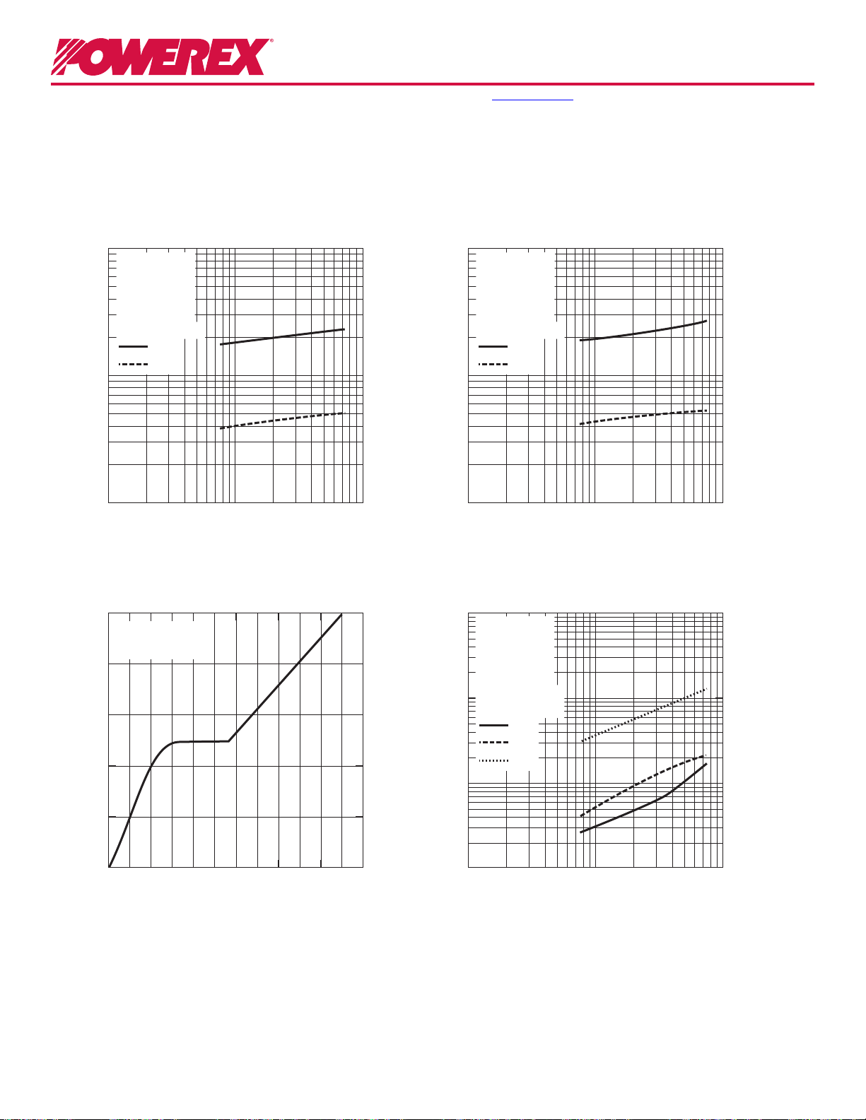
OUTPUT CHARACTERISTICS
(INVERTER PART - TYPICAL)
150
VGE = 20V
125
100
, (AMPERES)
C
15
75
50
25
COLLECTOR CURRENT, I
0
0 2 4 6 8 10
COLLECTOR-EMITTER VOLTAGE, VCE, (VOLTS)
FREE-WHEEL DIODE
FORWARD CHARACTERISTICS
(INVERTER PART - TYPICAL)
3
10
Tj = 25°C
= 125°C
T
j
= 150°C
T
j
(Chip)
, (AMPERES)
E
2
10
11
10
9
8
Tj = 25°C
(Chip)
SATURATION VOLTAGE CHARACTERISTICS
(INVERTER PART - TYPICAL)
4.5
Tj = 25°C
T
T
(Chip)
, (VOLTS)
CE(sat)
4.0
3.5
3.0
2.5
2.0
1.5
COLLECTOR-EMITTER
1.0
0.5
SATURATION VOLTAGE, V
0
0
COLLECTOR CURRENT, IC, (AMPERES)
(INVERTER PART - TYPICAL)
2
10
, (nF)
10
res
, C
oes
, C
ies
10
VGE = 0V
1
0
COLLECTOR-EMITTER
= 125°C
j
= 150°C
j
CAPACITANCE VS. V
CE
C
C
15075 100 12525 50
ies
oes
EMITTER CURRENT, I
1
10
0 1 3 652 4
EMITTER-COLLECTOR VOLTAGE, V
6
, (VOLTS)
EC
-1
10
CAPACITANCE, C
-2
10
-1
10
COLLECTOR-EMITTER VOLTAGE, VCE, (VOLTS)
10
C
res
0
10
1
10
2
02/14 Rev. 1
Page 7

Powerex, Inc., 173 Pavilion Lane, Youngwood, Pennsylvania 15697 (724) 925-7272 www.pwrx.com
CM75RX-34SA
Six IGBT + Brake NX-Series Module
75 Amperes/1700 Volts
SWITCHING CHARACTERISTICS
(INVERTER PART - TYPICAL)
4
10
3
10
2
10
10
10
1
0
10
VCC = 1000V
V
= ±15V
GE
R
= 10Ω
G
T
= 125°C
j
Inductive Load
0
COLLECTOR CURRENT, I
SWITCHING TIME, (ns)
(INVERTER PART - TYPICAL)
4
10
HALF-BRIDGE
t
d(off)
t
f
t
d(on)
t
r
1
10
, (AMPERES)
C
SWITCHING TIME VS.
GATE RESISTANCE
10
SWITCHING CHARACTERISTICS
HALF-BRIDGE
(INVERTER PART - TYPICAL)
4
10
3
10
2
10
SWITCHING TIME, (ns)
10
2
10
VCC = 1000V
1
V
GE
R
G
T
= 150°C
j
Inductive Load
0
0
10
= ±15V
= 10Ω
COLLECTOR CURRENT, IC, (AMPERES)
t
d(off)
t
d(on)
t
f
t
r
10
1
10
2
SWITCHING TIME VS.
GATE RESISTANCE
(INVERTER PART - TYPICAL)
4
10
3
10
10
SWITCHING TIME, (ns)
10
02/14 Rev. 1
2
1
t
f
t
d(on)
t
r
-1
10
EXTERNAL GATE RESISTANCE, RG, (Ω)
10
t
d(off)
VCC = 1000V
V
= ±15V
GE
I
= 75A
C
T
= 125°C
j
Inductive Load
0
10
1
10
2
3
10
10
SWITCHING TIME, (ns)
10
2
1
t
f
t
d(on)
t
r
-1
10
EXTERNAL GATE RESISTANCE, R
10
0
t
d(off)
VCC = 1000V
V
= ±15V
GE
I
= 75A
C
T
= 150°C
j
Inductive Load
1
10
, (Ω)
G
10
2
7
Page 8
Powerex, Inc., 173 Pavilion Lane, Youngwood, Pennsylvania 15697 (724) 925-7272 www.pwrx.com
CM75RX-34SA
Six IGBT + Brake NX-Series Module
75 Amperes/1700 Volts
REVERSE RECOVERY CHARACTERISTICS
(INVERTER PART - TYPICAL)
3
10
VCC = 1000V
V
= ±15V
GE
R
= 10Ω
(ns)
rr
(A), t
rr
10
REVERSE RECOVERY, I
10
G
T
= 125°C
j
Inductive Load
2
1
0
10
I
rr
t
rr
EMITTER CURRENT, IE, (AMPERES)
GATE CHARGE VS. V
20
IC = 75A
V
= 1000V
CC
16
, (VOLTS)
GE
12
8
1
10
(INVERTER PART)
GE
10
REVERSE RECOVERY CHARACTERISTICS
(INVERTER PART - TYPICAL)
3
10
(ns)
rr
(A), t
rr
10
REVERSE RECOVERY, I
10
2
VCC = 1000V
V
GE
R
= 10Ω
G
T
= 150°C
j
Inductive Load
2
1
0
10
= ±15V
I
rr
t
rr
10
EMITTER CURRENT, I
1
, (AMPERES)
E
10
2
HALF-BRIDGE SWITCHING
CHARACTERISTICS
(INVERTER PART - TYPICAL)
10
, (mJ)
off
, E
10
on
10
3
VCC = 1000V
V
= ±15V
GE
R
= 10Ω
G
T
= 125°C
j
Inductive Load,
2
Per Pulse
1
E
on
E
off
E
rr
10
10
10
2
1
0
, (mJ)
rr
4
GATE-EMITTER VOLTAGE, V
0
100 600500300 400200
0
8
GATE CHARGE, QG, (nC)
SWITCHING ENERGY, E
0
10
0
10
COLLECTOR CURRENT, IC, (AMPERES)
EMITTER CURRENT, IE, (AMPERES)
10
REVERSE RECOVERY ENERGY, E
-1
1
10
10
2
02/14 Rev. 1
Page 9

Powerex, Inc., 173 Pavilion Lane, Youngwood, Pennsylvania 15697 (724) 925-7272 www.pwrx.com
CM75RX-34SA
Six IGBT + Brake NX-Series Module
75 Amperes/1700 Volts
HALF-BRIDGE SWITCHING
(INVERTER PART - TYPICAL)
3
10
VCC = 1000V
V
= ±15V
GE
R
= 10Ω
, (mJ) SWITCHING ENERGY, E
off
, E
10
on
10
SWITCHING ENERGY, E
10
G
T
= 150°C
j
Inductive Load,
2
Per Pulse
1
0
0
10
COLLECTOR CURRENT, IC, (AMPERES)
E
on
E
off
E
rr
EMITTER CURRENT, IE, (AMPERES)
HALF-BRIDGE SWITCHING
(INVERTER PART - TYPICAL)
2
10
CHARACTERISTICS
1
10
CHARACTERISTICS
10
10
10
10
10
2
2
, (mJ)
rr
1
0
REVERSE RECOVERY ENERGY, E
-1
2
10
, (mJ)
rr
, (mJ)
off
, E
on
1
10
VCC = 1000V
V
= ±15V
GE
I
= 75A
C
T
= 125°C
SWITCHING ENERGY, E
REVERSE RECOVERY ENERGY, E
10
j
Inductive Load,
Per Pulse
0
1
10
EXTERNAL GATE RESISTANCE, RG, (Ω)
IMPEDANCE CHARACTERISTICS
(INVERTER PART - MAXIMUM)
0
th(j-c')
10
HALF-BRIDGE SWITCHING
CHARACTERISTICS
(INVERTER PART - TYPICAL)
2
10
TRANSIENT THERMAL
E
on
E
off
E
rr
3
10
, (mJ)
rr
, (mJ)
off
, E
on
1
10
VCC = 1000V
V
= ±15V
GE
I
= 75A
C
T
= 150°C
j
REVERSE RECOVERY ENERGY, E
10
Inductive Load,
Per Pulse
0
1
10
EXTERNAL GATE RESISTANCE, RG, (Ω)
10
-1
10
Single Pulse
T
= 25°C
C
Per Unit Base =
R
=
• (NORMALIZED VALUE)
-2
10
th
= R
E
on
E
off
E
rr
2
10
3
th
Z
-3
10
NORMALIZED TRANSIENT THERMAL IMPEDANCE, Z
10
-5
10
-3
-4
10
10-210-110010
TIME, (s)
th(j-c)
0.18 K/W
(IGBT)
R
=
th(j-c)
0.27 K/W
(FWDi)
1
02/14 Rev. 1
9
Page 10

Powerex, Inc., 173 Pavilion Lane, Youngwood, Pennsylvania 15697 (724) 925-7272 www.pwrx.com
CM75RX-34SA
Six IGBT + Brake NX-Series Module
75 Amperes/1700 Volts
SATURATION VOLTAGE CHARACTERISTICS
(BRAKE PART - TYPICAL)
4.5
Tj = 25°C
T
T
(Chip)
, (VOLTS)
CE(sat)
4.0
3.5
3.0
2.5
2.0
1.5
COLLECTOR-EMITTER
1.0
0.5
SATURATION VOLTAGE, V
0
0
COLLECTOR CURRENT, IC, (AMPERES)
SWITCHING CHARACTERISTICS
(BRAKE PART - TYPICAL)
4
10
10
10
VCC = 1000V
V
GE
R
= 13Ω
G
3
T
= 125°C
j
Inductive Load
2
= ±15V
COLLECTOR-EMITTER
= 125°C
j
= 150°C
j
HALF-BRIDGE
t
d(off)
t
f
t
d(on)
FREE-WHEEL DIODE
FORWARD CHARACTERISTICS
(BRAKE PART - TYPICAL)
2
10
(Chip)
, (VOLTS)
F
1
10
FORWARD VOLTAGE, V
0
10
1007525 50
0 2 3 4 51 6
FORWARD CURRENT I
Tj = 25°C
= 125°C
T
j
= 150°C
T
j
, (AMPERES)
F
HALF-BRIDGE
SWITCHING CHARACTERISTICS
(BRAKE PART - TYPICAL)
4
10
t
10
10
3
2
d(off)
t
f
t
d(on)
t
r
SWITCHING TIME, (ns)
10
10
10
1
0
0
10
COLLECTOR CURRENT, I
10
10
1
0
10
VCC = 1000V
V
= ±15V
GE
R
= 13Ω
G
T
= 150°C
j
Inductive Load
0
COLLECTOR CURRENT, IC, (AMPERES)
10
1
10
2
02/14 Rev. 1
t
r
10
1
C
, (AMPERES)
10
2
SWITCHING TIME, (ns)
Page 11

Powerex, Inc., 173 Pavilion Lane, Youngwood, Pennsylvania 15697 (724) 925-7272 www.pwrx.com
CM75RX-34SA
Six IGBT + Brake NX-Series Module
75 Amperes/1700 Volts
4
10
3
10
2
10
SWITCHING TIME, (ns)
1
10
1
10
EXTERNAL GATE RESISTANCE, R
HALF-BRIDGE SWITCHING
(BRAKE PART - TYPICAL)
2
10
SWITCHING TIME VS.
GATE RESISTANCE
(BRAKE - TYPICAL)
t
d(off)
t
d(on)
t
f
t
r
VCC = 1000V
V
GE
I
= 50A
C
T
= 125°C
j
Inductive Load
2
10
CHARACTERISTICS
= ±15V
, (Ω)
G
10
3
10
SWITCHING TIME VS.
GATE RESISTANCE
(BRAKE - TYPICAL)
4
10
t
10
t
t
t
r
2
d(off)
d(on)
f
VCC = 1000V
V
= ±15V
GE
I
= 50A
C
T
= 150°C
j
Inductive Load
10
3
3
10
2
10
SWITCHING TIME, (ns)
1
10
1
10
EXTERNAL GATE RESISTANCE, RG, (Ω)
HALF-BRIDGE SWITCHING
CHARACTERISTICS
(BRAKE PART - TYPICAL)
1
10
2
10
1
, (mJ)
off
, E
on
10
1
VCC = 1000V
V
= ±15V
GE
R
= 13Ω
G
T
= 125°C
j
Inductive Load,
Per Pulse
E
SWITCHING ENERGY, E
0
10
0
10
on
E
off
E
rr
COLLECTOR CURRENT, IC, (AMPERES)
FORWARD CURRENT, IF, (AMPERES)
10
10
, (mJ)
rr
, (mJ)
off
, E
on
0
10
1
VCC = 1000V
V
= ±15V
GE
R
= 13Ω
G
T
= 150°C
j
10
, (mJ)
rr
0
Inductive Load,
Per Pulse
E
SWITCHING ENERGY, E
REVERSE RECOVERY ENERGY, E
-1
1
10
10
2
10
0
0
10
on
E
off
E
rr
1
10
COLLECTOR CURRENT, IC, (AMPERES)
FORWARD CURRENT, IF, (AMPERES)
10
REVERSE RECOVERY ENERGY, E
-1
10
2
02/14 Rev. 1
11
Page 12

Powerex, Inc., 173 Pavilion Lane, Youngwood, Pennsylvania 15697 (724) 925-7272 www.pwrx.com
CM75RX-34SA
Six IGBT + Brake NX-Series Module
75 Amperes/1700 Volts
HALF-BRIDGE SWITCHING
CHARACTERISTICS
(BRAKE PART - TYPICAL)
2
10
, (mJ)
rr
, (mJ)
off
, E
on
1
10
SWITCHING ENERGY, E
REVERSE RECOVERY ENERGY, E
0
10
1
10
EXTERNAL GATE RESISTANCE, R
REVERSE RECOVERY CHARACTERISTICS
(BRAKE PART - TYPICAL)
3
10
VCC = 1000V
V
= ±15V
GE
R
= 13Ω
(ns)
rr
(A), t
rr
G
T
= 125°C
j
Inductive Load
10
VCC = 1000V
V
I
C/IF
T
j
Inductive Load,
Per Pulse
2
= ±15V
GE
= 50A
= 125°C
E
on
E
off
E
rr
, (Ω)
G
10
10
, (mJ)
rr
, (mJ)
off
, E
on
10
SWITCHING ENERGY, E
REVERSE RECOVERY ENERGY, E
3
10
10
(ns)
rr
(A), t
rr
HALF-BRIDGE SWITCHING
CHARACTERISTICS
(BRAKE PART - TYPICAL)
2
VCC = 1000V
V
1
= ±15V
GE
I
= 50A
C/IF
T
= 150°C
j
Inductive Load,
Per Pulse
E
on
E
off
E
0
1
10
EXTERNAL GATE RESISTANCE, RG, (Ω)
10
2
rr
REVERSE RECOVERY CHARACTERISTICS
(BRAKE PART - TYPICAL)
3
VCC = 1000V
V
= ±15V
GE
R
= 13Ω
G
T
= 150°C
j
Inductive Load
10
3
2
10
REVERSE RECOVERY, I
1
10
10
12
0
FORWARD CURRENT, I
10
1
, (AMPERES)
F
2
10
I
rr
t
rr
2
10
REVERSE RECOVERY, I
1
10
0
10
FORWARD CURRENT, IF, (AMPERES)
10
1
I
rr
t
rr
2
10
02/14 Rev. 1
Page 13

Powerex, Inc., 173 Pavilion Lane, Youngwood, Pennsylvania 15697 (724) 925-7272 www.pwrx.com
CM75RX-34SA
Six IGBT + Brake NX-Series Module
75 Amperes/1700 Volts
TRANSIENT THERMAL
th(j-c')
10
IMPEDANCE CHARACTERISTICS
(BRAKE PART - MAXIMUM)
0
10
TEMPERATURE CHARACTERISTICS
(NTC THERMISTOR PART - TYPICAL)
2
-1
10
Single Pulse
T
= 25°C
C
Per Unit Base =
R
=
• (NORMALIZED VALUE)
-2
10
th
= R
th
Z
th(j-c)
0.25 K/W
(IGBT)
R
=
th(j-c)
0.35 K/W
(FWDi)
-3
10
-5
NORMALIZED TRANSIENT THERMAL IMPEDANCE, Z
10
10
-4
-3
10
10-210-110010
TIME, (s)
1
10
0
10
RESISTANCE, R (kΩ)
-1
10
1
-50 25 50 100750-25
125
TEMPERATURE, T (°C)
02/14 Rev. 1
13
 Loading...