

Page 1
CM400E3Y6-24NFH
Powerex, Inc., 173 Pavilion Lane, Youngwood, Pennsylvania 15697 (724) 925-7272
www.pwrx.com
A
M
K
N
P
H
B
(4 PLACES)
Q
LABEL
Di2
D
W W
Q
Di1
E2
NTC
F F
E
C2E1 E2 C1
Q
R
C
S T T U
W
X X X
Tr 2
C2E1
C1
G2
G
E2
H
E1
G1
G
J
V NUTS (3 PLACES)
Y
Z
AA
G2
E2
E1 (TH2)
G1 (TH1)
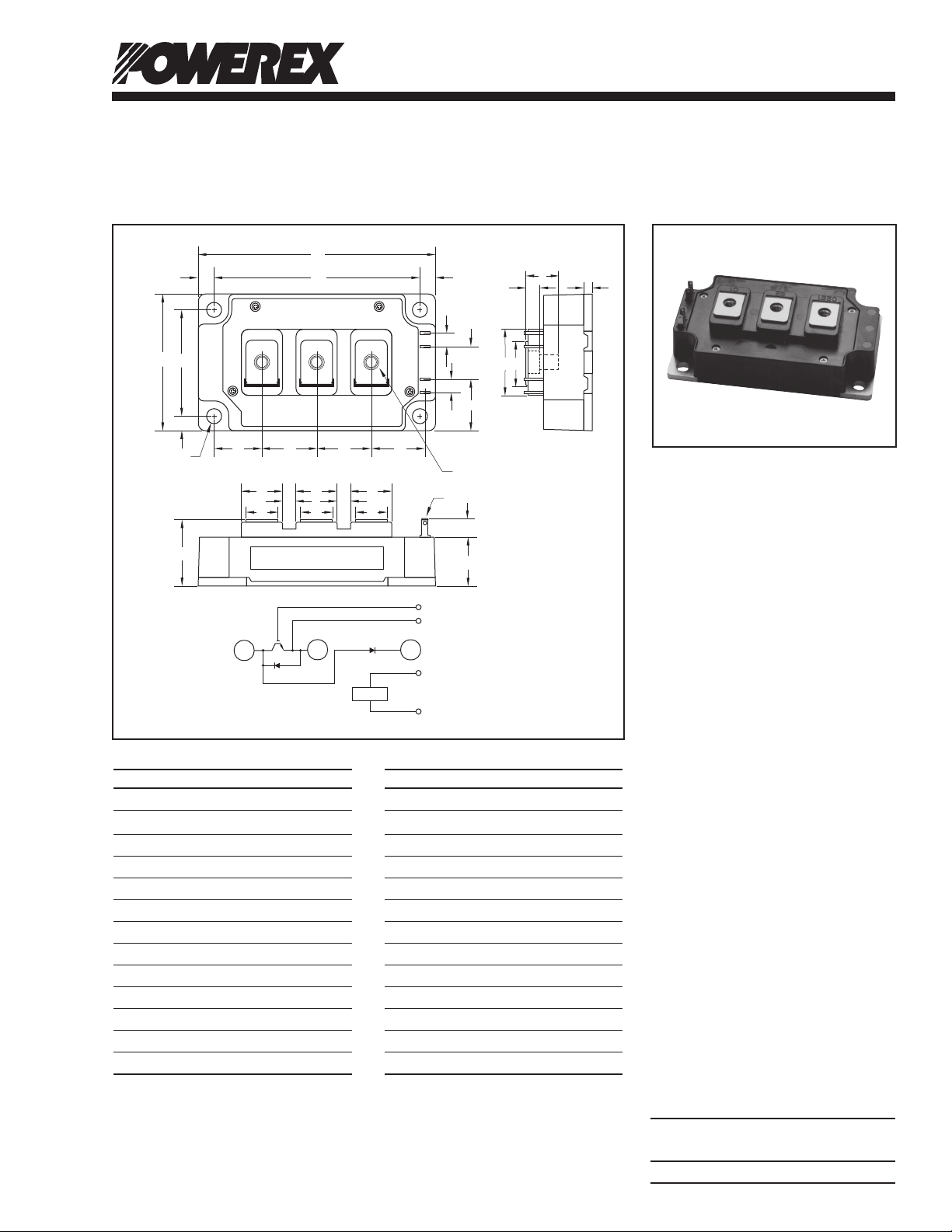
Outline Drawing and Circuit Diagram
Dimensions Inches Millimeters
A 4.25 108.0
B 2.44 62.0
C 1.18+0.4/-0.02 30.0+1.0/-0.5
D 3.66±0.01 93.0±0.25
E 1.89±0.01 48.0±0.25
F 0.29 7.5
G 0.24 6.0
J 0.689 17.5
H 0.59 15.0
K 0.244 6.2
L 0.16 4.0
M 0.56 14.2
N 1.18 30.0
Dimensions Inches Millimeters
P 0.79 20.0
Q 0.28 7.0
R 0.26 Dia. Dia. 6.5
S 0.85 21.5
T 0.98 25.0
U 0.94 24.0
V M6 Metric M6
V 0.16 4.0
W 0.71 18.0
X 0.55 14.0
Y 0.02 0.5
Z 0.33 8.5
AA 0.87 22.2
Chopper IGBTMOD™
NFH-Series Module
400 Amperes/1200 Volts
L
Description:
Powerex IGBTMOD™ Modules
are designed for use high
frequency applications; 30 kHz for
hard switching applications and
60 to 70 kHz for soft switching
applications. Each module
consists of two IGBT Transistors
in a half-bridge configuration with
each transistor having a reverseconnected super-fast recovery
free-wheel diode. All components
and interconnects are isolated from
the heat sinking baseplate, offering
simplified system assembly and
thermal management.
Features:
£ Low E
£ Discrete Super-Fast Recovery
£ Isolated Baseplate for Easy
Applications:
£ Power Supplies
£ Induction Heating
£ Welders
Ordering Information:
Example: Select the complete
module number you desire from
the table below -i.e.
CM400E3Y6-24NFH is a 1200V
(V
CES
IGBTMOD™ Power Module.
SW(off)
Free-Wheel Diode
Heat Sinking
), 400 Ampere Chopper
Type Current Rating
V
CES
Amperes Volts (x 50)
CM 400 24
112/11 Rev. 0
Page 2
Powerex, Inc., 173 Pavilion Lane, Youngwood, Pennsylvania 15697 (724) 925-7272 www.pwrx.com
CM400E3Y6-24NFH
Chopper IGBTMOD™ NFH-Series Module
400 Amperes/1200 Volts
Absolute Maximum Ratings, Tj = 25°C unless otherwise specied
Inverter IGBT/FWDi Part
Characteristics Symbol Rating Units
Collector-Emitter Voltage (VGE = 0V) V
Gate-Emitter Voltage (VCE = 0V) V
1200 Volts
CES
±20 Volts
GES
Collector Current (Operation, TC = 25°C)*3 IC 400 Amperes
Collector Current (Pulse, Repetitive)*2 I
Total Power Dissipation (TC = 25°C)
*2,*3
P
Emitter Current (Operation, TC = 25°C)*3 I
Emitter Current (Pulse, Repetitive)*2 I
800 Amperes
CRM
2190 Watts
tot
*1
50 Amperes
E
*1
100 Amperes
ERM
Clamp Diode Part
Characteristics Symbol Rating Units
Repetitive Peak Reverse Voltage V
Forward Current (Operation, TC = 25°C)*3 IF 400 Amperes
Forward Current (Pulse, Repetitive)*2 I
1200 Volts
RRM
800 Amperes
FRM
Module
Characteristics Symbol Rating Units
Isolation Voltage (Charged Part to Baseplate, f= 60 Hz, AC 1 Minute) V
Maximum Junction Temperature T
Operating Junction Temperature T
Storage Temperature T
*1 Represent ratings and characteristics of the anti-parallel, emitter-to-collector free wheeling diode (FWDi).
*2 Pulse width and repetition rate should be such that device junction temperature (Tj) does not exceed T
*3 Case temperature (TC) and heatsink temperature (Ts) is measured on the surface (mounting side) of the baseplate and the heatsink side just under the chips.
Refer to the figure to the right for chip location. The heatsink ther mal resistance should be measured just under the chips.
0 60.1
0
18.4
30.4
34.4
0 77.042.231.8
Each mark points to the center position of each chip.
Tr2: IGBT Di2: FWDi
Di1: ClampDi Th: NTC Thermistor
Th
Di1
Tr2Tr2
Di2
52.4
Di1
LABEL SIDE
0
24.4
34.5
j(max)
rating.
2500 V
ISO
+150 °C
j(max)
-40 to +150 °C
j(op)
-40 to +125 °C
stg
rms
2 12/11 Rev. 0
Page 3

Powerex, Inc., 173 Pavilion Lane, Youngwood, Pennsylvania 15697 (724) 925-7272 www.pwrx.com
CM400E3Y6-24NFH
Chopper IGBTMOD™ NFH-Series Module
400 Amperes/1200 Volts
Electrical Characteristics, Tj = 25°C unless otherwise specied
Inverter IGBT/FWDi Part
Characteristics Symbol Test Conditions Min. Typ. Max. Units
Collector-Emitter Cutoff Current I
Gate-Emitter Leakage Current I
Gate-Emitter Threshold Voltage V
Collector-Emitter Saturation Voltage V
IC = 400A, VGE = 15V, Tj = 125°C*4 — 5.0 — Volts
Input Capacitance C
Output Capacitance C
Reverse Transfer Capacitance C
Total Gate Charge QG VCC = 600V, IC = 400A, VGE = 15V — 1800 — nC
Turn-on Delay Time t
Rise Time tr VCC = 600V, IC = 400A, VGE = ±15V, — — 100 ns
Turn-off Delay Time t
Fall Time tf — — 150 ns
Emitter-Collector Voltage V
Internal Lead Resistance R
Chip - Terminals
Internal Gate Resistance rg TC = 25°C — 0.8 — Ω
External Gate Resistance RG 0.78 — 7.8 Ω
VCE = V
CES
±VGE = V
GES
IC = 40mA, VCE = 10V 4.5 6.0 7.5 Volts
GE(th)
IC = 400A, VGE = 15V, Tj = 25°C*4 — 5.0 6.5 Volts
CE(sat)
— — 63 nF
ies
VCE = 10V, VGE = 0V — — 5.3 nF
oes
— — 1.2 nF
res
— — 300 ns
d(on)
RG = 0.78Ω, Inductive Load — — 500 ns
d(off)
*1
IE = 50A, VGE = 0V*4 — 2.8 3.8 Volts
EC
CC' + EE'
IC = 400A, TC = 25°C, — 0.53 — mΩ
, VGE = 0V — — 1 mA
CES
, VCE = 0V — — 1 µA
GES
Clamp Diode Part
Collector Cutoff Current I
Reverse Recovery Time trr VCC = 600V, IF = 400A, VGE = ±15V, — — 100 ns
Reverse Recovery Charge Qrr RG = 0.78Ω, Inductive Load — 7.0 — µC
Emitter-Collector Voltage VFM IF = 400A*4 — 5.5 7.0 Volts
Internal Lead Resistance R
Chip - Terminals
*1 Represent ratings and characteristics of the anti-parallel, emitter-to-collector free wheeling diode (FWDi).
*4 Pulse width and repetition rate should be such as to cause negligible temperature rise.
VR = V
RRM
CC' + EE'
IF = 400A, TC = 25°C, — 0.53 — mΩ
— — 1 mA
RRM
312/11 Rev. 0
Page 4

Powerex, Inc., 173 Pavilion Lane, Youngwood, Pennsylvania 15697 (724) 925-7272 www.pwrx.com
CM400E3Y6-24NFH
Chopper IGBTMOD™ NFH-Series Module
400 Amperes/1200 Volts
Electrical Characteristics, Tj = 25°C unless otherwise specied
NTC Thermistor Part
Characteristics Symbol Test Conditions Min. Typ. Max. Units
Zero Power Resistance R25 TC = 25°C*3 4.85 5.00 5.15 kΩ
Deviation of Resistance ∆R/R R
B Constant B
Approximate by Equation*5 — 3375 — K
(25/50)
= 493Ω, TC = 100°C*3 -7.3 — +7.8 %
100
Power Dissipation P25 TC = 25°C*3 — — 10 mW
Mechanical Characteristics
Mounting Torque Mt Main Terminals, M6 Screw 31 35 40 in-lb
Mounting Torque Ms Mounting, M6 Screw 31 35 40 in-lb
Weight m — 400 — Grams
Flatness of Baseplate ec On Centerline X, Y*6 -100 — +100 µm
Thermal Resistance Characteristics, Tj = 25°C unless otherwise specied
Thermal Resistance, Junction to Case R
Thermal Resistance, Junction to Case R
Thermal Resistance, Junction to Case R
Contact Thermal Resistance, R
Case to Heatsink*2 per 1/2 Module
*3 Case temperature (TC) is measured on the surface (mounting side) of the baseplate just under the chips.
Refer to the figure to the right for chip location.
*5 B
(25/50)
R
R25; Resistance at Absolute Temperature T25 [K]; T25 = 25 [°C] + 273.15 = 298.15 [K]
R50; Resistance at Absolute Temperature T50 [K]; T50 = 50 [°C] + 273.15 = 323.15 [K]
*6 Baseplate (mounting side) flatness measurement points (X, Y) are shown in the figure.
= In(
R
25
)/( 1 –
50 T25 T50
1
)
+ CONVEX
– CONCAVE
Y
X
Q Per Inver ter IGBT*3 — — 0.057 K/W
th(j-c)
D Per Inverter FWDi*3 — — 0.430 K/W
th(j-c)
D Per ClampDi*3 — — 0.098 K/W
th(j-c)
Thermal Grease Applied, — 0.02 — K/W
th(c-s)
*3,*7
0 60.1
0
BOTTOM
18.4
30.4
34.4
3 mm
Th
Di1
Tr2Tr2
Di2
Di1
0
24.4
34.5
HEATSINK SIDE
HEATSINK SIDE
*7 Typical value is measured by using thermally conductive grease of λ = 0.9 [W/(m • K)].
– CONCAVE
+ CONVEX
0 77.042.231.8
Each mark points to the center position of each chip.
Tr2: IGBT Di2: FWDi
Di1: ClampDi Th: NTC Thermistor
52.4
LABEL SIDE
4 12/11 Rev. 0
 Loading...