

Page 1
CM400DY-12NF
A
XW
FF
B
N
L
(4 PLACES)
D
M NUTS
(3 PLACES)
G
G
H
KKK
P P
P
T THICK
U WIDTH
QQ
V
C
S
R
G2
E2
E1
G1
C1E2C2E1
T
C
MEASURED POINT
(BASEPLATE)
LABEL
C2E1 E2 C1
G2
E2
E1
G1
E
Powerex, Inc., 200 E. Hillis Street, Youngwood, Pennsylvania 15697-1800 (724) 925-7272
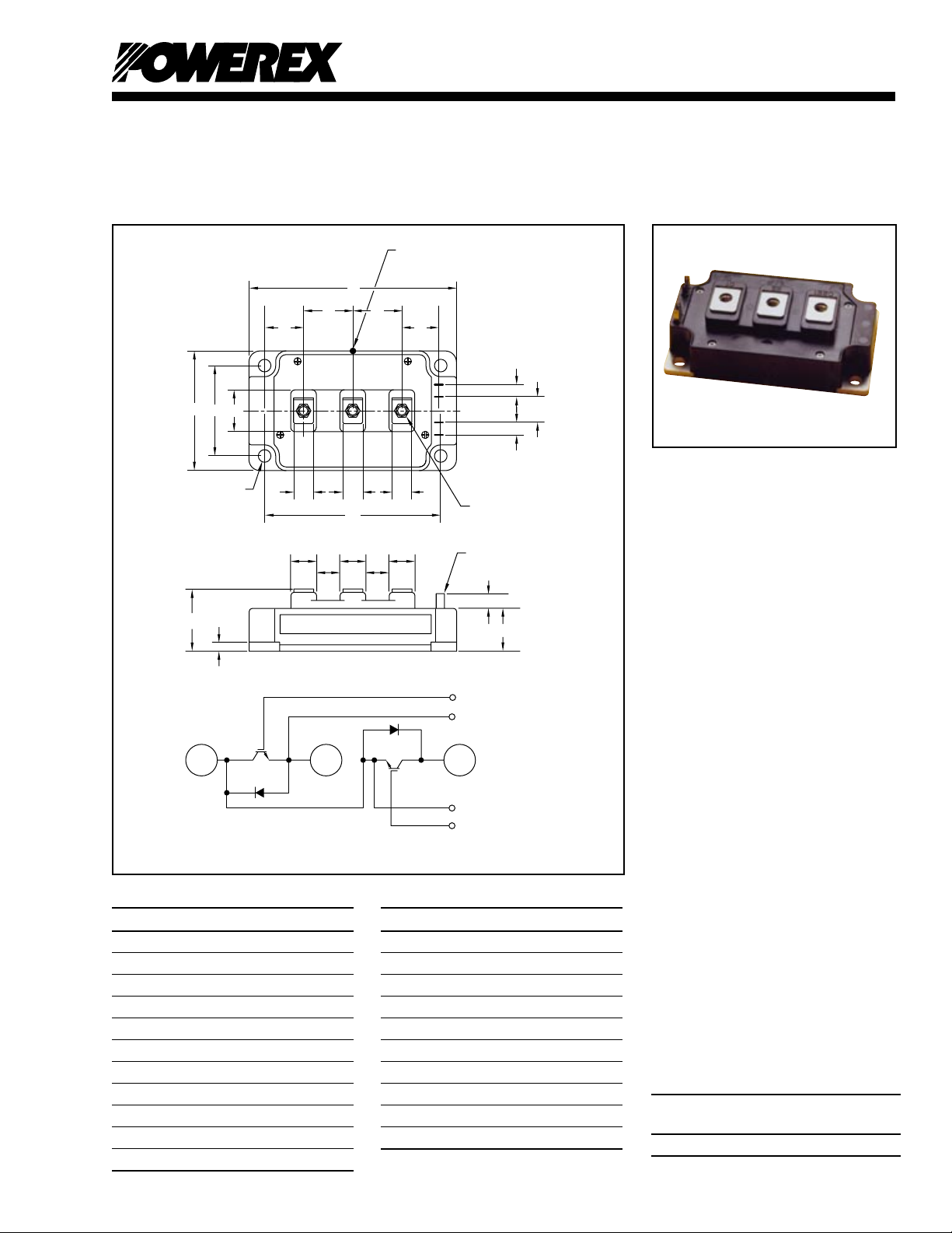
Dual IGBTMOD™
NF-Series Module
400 Amperes/600 Volts
Description:
Powerex IGBTMOD™ Modules
are designed for use in switching
applications. Each module consists
of two IGBT Transistors in a halfbridge conguration with each transistor having a reverse-connected
super-fast recovery free-wheel
diode. All components and interconnects are isolated from the heat
sinking baseplate, offering simplied system assembly and thermal
management.
Features:
£ Low Drive Power
£ Low V
CE(sat)
£ Discrete Super-Fast Recovery
Free-Wheel Diode
£ Isolated Baseplate for Easy
Heat Sinking
Applications:
Outline Drawing and Circuit Diagram
Dimensions Inches Millimeters
A 4.25 108.0
B 2.44 62.0
C 1.18+0.04/-0.02 30.0+1.0/-0.5
D 3.66±0.01 93.0±0.25
E 1.89±0.01 48.0±0.25
F 0.98 25.0
G 0.24 6.0
H 0.59 15.0
K 0.55 14.0
L 0.26 Dia. Dia. 6.5
M M6 Metric M6
Dimensions Inches Millimeters
N 1.18 30.0
P 0.71 18.0
Q 0.28 7.0
R 0.87 22.2
S 0.33 8.5
T 0.02 0.5
U 0.110 2.8
V 0.16 4.0
W 0.85 21.5
X 0.94 24.0
£ AC Motor Control
£ UPS
£ Battery Powered Supplies
Ordering Information:
Example: Select the complete
part module number you desire
from the table below -i.e.
CM400DY-12NF is a 600V (V
400 Ampere Dual IGBTMOD™
Power Module.
Type Current Rating
Amperes Volts (x 50)
CM 400 12
CES
V
CES
),
1
Page 2

Powerex, Inc., 200 E. Hillis Street, Youngwood, Pennsylvania 15697-1800 (724) 925-7272
3
CM400DY-12NF
Dual IGBTMOD™ NF-Series Module
400 Amperes/600 Volts
Powerex, Inc., 200 E. Hillis Street, Youngwood, Pennsylvania 15697-1800 (724) 925-7272
CM400DY-12NF
Dual IGBTMOD™ NF-Series Module
400 Amperes/600 Volts
Absolute Maximum Ratings, Tj = 25 °C unless otherwise specied
Ratings Symbol CM400DY-12NF Units
Junction Temperature Tj –40 to 150 °C
Storage Temperature T
Collector-Emitter Voltage (G-E Short) V
Gate-Emitter Voltage (C-E Short) V
Collector Current*** (DC, T
' = 92°C) I
C
–40 to 125 °C
stg
600 Volts
CES
±20 Volts
GES
C
400 Amperes
Peak Collector Current ICM 800* Amperes
Emitter Current** (TC = 25°C) IE 400 Amperes
Peak Emitter Current** IEM 800* Amperes
Maximum Collector Dissipation (TC = 25°C, Tj ≤ 150°C) PC 1130 Watts
Mounting Torque, M6 Main Terminal — 40 in-lb
Mounting Torque, M6 Mounting — 40 in-lb
Weight — 400 Grams
Isolation Voltage (Main Terminal to Baseplate, AC 1 min.) V
.
2500 Volts
ISO
Static Electrical Characteristics, Tj = 25 °C unless otherwise specied
Characteristics Symbol Test Conditions Min. Typ. Max. Units
Collector-Cutoff Current I
Gate Leakage Current I
Gate-Emitter Threshold Voltage V
Collector-Emitter Saturation Voltage V
IC = 400A, VGE = 15V, Tj = 125°C — 1.7 — Volts
Total Gate Charge QG VCC = 300V, IC = 400A, VGE = 15V — 1600 — nC
Emitter-Collector Voltage** VEC IE = 400A, VGE = 0V — — 2.6 Volts
VCE = V
CES
VGE = V
GES
IC = 40mA, VCE = 10V 5.0 6.0 7.5 Volts
GE(th)
IC = 400A, VGE = 15V, Tj = 25°C — 1.7 2.2 Volts
CE(sat)
, VGE = 0V — — 1.0 mA
CES
, VCE = 0V — — 0.5 µA
GES
Dynamic Electrical Characteristics, Tj = 25 °C unless otherwise specied
Characteristics Symbol Test Conditions Min. Typ. Max. Units
Input Capacitance C
Output Capacitance C
Reverse Transfer Capacitance C
Inductive Turn-on Delay Time t
— — 60 nf
ies
VCE = 10V, VGE = 0V — — 7.3 nf
oes
— — 2.4 nf
res
— — 300 ns
d(on)
Load Rise Time tr VCC = 300V, IC = 400A, — — 200 ns
Switch Turn-off Delay Time t
d(off)
V
GE1
= V
= 15V, RG = 3.1Ω, — — 450 ns
GE2
Time Fall Time tf Inductive Load — — 300 ns
Diode Reverse Recovery Time** trr Switching Operation, — — 250 ns
Diode Reverse Recovery Charge** Qrr IE = 400A — 6.8 — µC
*Pulse width and repetition rate should be such that device junction temperature (Tj) does not exceed T
**Represents characteristics of the anti-parallel, emitter-to-collector free-wheel diode (FWDi)
***Tc' measured point is just under the chips. If this vaule is used, Rth(f-a) should be measured just under the chips .
j(max)
rating.
2
Page 3
Powerex, Inc., 200 E. Hillis Street, Youngwood, Pennsylvania 15697-1800 (724) 925-7272
COLLECTOR-EMITTER VOLTAGE, VCE, (VOLTS)
CAPACITANCE, C
ies
, C
oes
, C
res
, (nF)
CAPACITANCE VS. V
CE
(TYPICAL)
10
0
10
2
10
2
10
1
10
0
10
-1
10
1
0 1 3 42 5
10
1
EMITTER-COLLECTOR VOLTAGE, VEC, (VOLTS)
FREE-WHEEL DIODE
FORWARD CHARACTERISTICS
(TYPICAL)
10
2
10
3
EMITTER CURRENT, I
E
, (AMPERES)
GATE-EMITTER VOLTAGE, VGE, (VOLTS)
COLLECTOR-EMITTER
SATURATION VOLTAGE,
V
CE(sat)
, (VOLTS)
COLLECTOR-EMITTER
SATURATION VOLTAGE CHARACTERISTICS
(TYPICAL)
10
6 8
10 1412 16 18 20
8
6
4
2
0
Tj = 25°C
COLLECTOR-CURRENT, IC, (AMPERES)
COLLECTOR-EMITTER
SATURATION VOLTAGE,
V
CE(sat)
, (VOLTS
)
COLLECTOR-EMITTER
SATURATION VOLTAGE CHARACTERISTICS
(TYPICAL)
4
3
0
200
600
2
1
0
800
VGE = 15V
Tj = 25°C
Tj = 125°C
VGE = 0V
C
ies
C
oes
C
res
IC = 800A
IC = 400A
IC = 160A
COLLECTOR-EMITTER VOLTAGE, VCE, (VOLTS)
COLLECTOR CURRENT, I
C
, (AMPERES)
OUTPUT CHARACTERISTICS
(TYPICAL)
0 2 4 6 8 10
200
0
VGE =
20V
10
11
12
15
13
9
8
Tj = 25
o
C
400
600
800
400
10
-1
COLLECTOR CURRENT, IC, (AMPERES)
10
3
10
1
10
2
10
2
10
0
10
1
SWITCHING TIME, (ns)
HALF-BRIDGE
SWITCHING CHARACTERISTICS
(TYPICAL)
t
d(off)
t
d(on)
t
r
VCC = 300V
VGE = ±15V
RG = 3.1Ω
Tj = 125°C
Inductive Load
t
f
10
3
Tj = 25°C
Tj = 125°C
CM400DY-12NF
Dual IGBTMOD™ NF-Series Module
400 Amperes/600 Volts
Thermal and Mechanical Characteristics, Tj = 25 °C unless otherwise specied
Characteristics Symbol Test Conditions Min. Typ. Max. Units
Thermal Resistance, Junction to Case R
Point per Outline Drawing
Thermal Resistance, Junction to Case R
Point per Outline Drawing
Thermal Resistance, Junction to Case R
TC Reference Point Under Chips
Contact Thermal Resistance R
External Gate Resistance RG 1.6 — 16 Ω
Q Per IGBT 1/2 Module, TC Reference — — 0.11 °C/W
th(j-c)
D Per FWDi 1/2 Module, TC Reference — — 0.19 °C/W
th(j-c)
'Q Per IGBT 1/2 Module, — — 0.066 °C/W
th(j-c)
Per 1/2 Module, Thermal Grease Applied — 0.04 — °C/W
th(c-f)
3
Page 4

Powerex, Inc., 200 E. Hillis Street, Youngwood, Pennsylvania 15697-1800 (724) 925-7272
TIME, (s)
TRANSIENT THERMAL
IMPEDANCE CHARACTERISTICS
(IGBT & FWDi)
10
0
10
-5
10
-4
10
-3
10
-1
10
-2
10
-3
10-310
-2
10
-1
10
0
10
1
10
-1
10
-2
10
-3
Z
th
= R
th
• (NORMALIZED VALUE)
Single Pulse
TC = 25°C
Per Unit Base =
R
th(j-c)
=
0.11°C/W
(IGBT)
R
th(j-c)
=
0.19°C/W
(FWDi)
NORMALIZED TRANSIENT THERMAL IMPEDANCE, Z
th(j-c')
GATE CHARGE, QG, (nC)
GATE-EMITTER VOLTAGE, V
GE
, (VOLTS)
GATE CHARGE VS. V
GE
20
0
16
12
8
4
0
500 1000 1500 25002000
VCC = 300V
EMITTER CURRENT, IE, (AMPERES)
REVERSE RECOVERY TIME, t
rr
, (ns)
REVERSE RECOVERY CHARACTERISTICS
(TYPICAL)
10
3
10
1
10
2
10
2
10
1
10
3
10
2
10
1
REVERSE RECOVERY CURRENT, I
rr
, (AMPERES)
VCC = 300V
VGE = ±15V
RG = 3.1Ω
Tj = 25°C
Inductive Load
VCC = 200V
IC = 400A
10
3
COLLECTOR CURRENT,
IC, (AMPERES)
SWITCHING LOSS, E
SW( on)
, E
SW( off)
, (mJ/PULSE)
10
2
10
1
10
2
10
1
10
0
VCC = 300V
VGE = ±15V
RG = 3.1Ω
Tj = 125°C
Inductive Load
C Snubber at Bus
VCC = 300V
VGE = ±15V
IC = 400A
Tj = 125°C
Inductive Load
C Snubber at Bus
10
3
SWITCHING LOSS VS.
COLLECTOR CURRENT (TYPICAL)
GATE RESISTANCE, RG, (Ω)
SWITCHING LOSS, E
SW( on)
, E
SW( off)
, (mJ/PULSE)
10
2
10
0
10
1
10
1
10
0
10
2
SWITCHING LOSS VS.
GATE RESISTANCE (TYPICAL)
E
SW(on)
E
SW(off)
E
SW(on)
E
SW(off)
I
rr
t
rr
CM400DY-12NF
Dual IGBTMOD™ NF-Series Module
400 Amperes/600 Volts
4
 Loading...