

Page 1
CM100TX-24S
Powerex, Inc., 173 Pavilion Lane, Youngwood, Pennsylvania 15697 (724) 925-7272
www.pwrx.com
AE
AC
A
E
F
G
K
K
JMMM T
52 51 50 49 48 47 46 45 44 43 42 41 40 39 38 37 36 35 34 33 32 31
H
L
X
53
54
K
55
K
56
57
58
59
K
60
K
61
12345678910111213141516171819202122
LLLLL
P(54~56)
UP(1)
G
E
UP(2)
U(48~50) V(42~44) W(36~38)
G
UN(5)
N(59~61)
K
K
D
DETAIL "A"
KQ
DETAIL "B"
VP(9)
G
E
VP(10)
G
VN(13)
K
K
K
K
KKKKKK
U
Y
K
K
G
E
G
EWN(22)EVN(14)EUN(6)
H
30
29
28
27
26
25
24
23
W
WP(17)
WP(18)
WN(21)
V
S
R B
L
N (4 PLACES)
P
P1(28~30)
N1(23~25)
TH1
(31)
AA
AB
K
AD
DETAIL "A"
C
Z
AJ
AH
AG
DETAIL "B"
TH
2
(32)
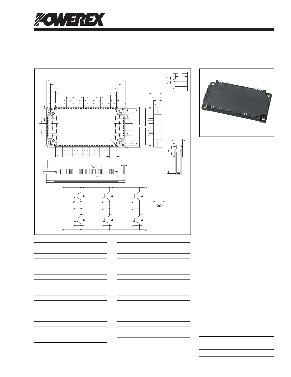
Outline Drawing and Circuit Diagram
Dimensions Inches Millimeters
A 4.79 121.7
B 2.44 62.0
C 0.51 13.0
D 4.65 118.1
E 4.33±0.02 110.0±0.5
F 3.9 99.0
G 3.72 94.5
H 0.61 15.415
J 1.125 28.575
K 0.15 3.81
L 0.45 11.43
M 0.6 15.24
N 0.22 Dia. 5.5 Dia.
P 2.30 58.4
Q 0.21 5.34
R 1.97±0.02 50.0±0.5
S 2.26 57.5
Dimensions Inches Millimeters
U 0.285 7.245
V 0.018 0.45
W 0.625 15.865
X 0.14 3.5
Y 0.03 0.8
Z 0.28 7.0
AA 0.81 20.5
AB 0.67 17.0
AC 0.03 0.65
AD 0.05 1.15
AE 0.29 7.4
AF 0.05 6.2
AG 0.49 12.5
AH 0.06 1.5
AJ 0.17 Dia. 4.3 Dia.
AK 0.10 Dia. 2.5 Dia.
AL 0.08 Dia. 2.1 Dia.
T 0.465 11.805
Six IGBTMOD™
NX-S Series Module
100 Amperes/1200 Volts
AF
AK
AL
Description:
Powerex IGBTMOD™ Modules
are designed for use in switching
applications. Each module
consists of six IGBT Transistors in
a three phase bridge configuration,
with each transistor having a
reverse-connected super-fast
recovery free-wheel diode. All
components and interconnects
are isolated from the heat sinking
baseplate, offering simplified
system assembly and thermal
management.
Features:
£ Low Drive Power
£ Low V
CE(sat)
£ Discrete Super-Fast Recovery
Free-Wheel Diode
£ Isolated Baseplate for Easy
Heat Sinking
Applications:
£ AC Motor Control
£ Motion/Servo Control
£ Photovoltaic/Fuel Cell
Ordering Information:
Example: Select the complete
module number you desire from
the table below -i.e.
CM100TX-24S is a 1200V (V
100 Ampere Six-IGBTMOD™ Power Module.
Type Current Rating
Amperes Volts (x 50)
CM 100 24
),
CES
V
CES
110/10 Rev. 1
Page 2

Powerex, Inc., 173 Pavilion Lane, Youngwood, Pennsylvania 15697 (724) 925-7272 www.pwrx.com
CM100TX-24S
Six IGBTMOD™ NX-S Series Module
100 Amperes/1200 Volts
Absolute Maximum Ratings, Tj = 25°C unless otherwise specied
Characteristics Symbol CM100TX-24S Units
Maximum Junction Temperature T
Operating Power Device Junction Temperature T
Storage Temperature T
+175 °C
j(max)
-40 to 150 °C
j(op)
-40 to 125 °C
stg
Mounting Torque, M5 Mounting Screws — 31 in-lb
Module Weight (Typical) — 270 Grams
Isolation Voltage (Terminals to Baseplate, f = 60Hz, AC 1 minute) V
2500 V
ISO
rms
Inverter Sector
Collector-Emitter Voltage (VGE = 0V) V
Gate-Emitter Voltage (VCE = 0V) V
Collector Current (DC, TC = 118°C)
*1,*5
IC 100 Amperes
Collector Current (Pulse)*4 I
Total Power Dissipation (TC = 25°C)
Emitter Current, Free Wheeling Diode Forward Current (TC = 25°C)
*1,*5
P
*1,*5
I
Emitter Current, Free Wheeling Diode Forward Current (Pulse)*4 I
*1 Case temperature (TC) and heatsink temperature (Tf) measured point is just under the chips.
*3 Represent ratings and characteristics of the anti-parallel, emitter-to-collector free wheeling diode (FWDi).
*4 Pulse width and repetition rate should be such that device junction temperature (Tj) does not exceed T
*5 Junction temperature (Tj) should not increase beyond maximum junction temperature (T
j(max)
) rating.
j(max)
rating.
1200 Volts
CES
±20 Volts
GES
200 Amperes
CRM
750 Watts
tot
*3
100 Amperes
E
*3
200 Amperes
ERM
2 10/10 Rev. 1
Page 3

Powerex, Inc., 173 Pavilion Lane, Youngwood, Pennsylvania 15697 (724) 925-7272 www.pwrx.com
CM100TX-24S
Six IGBTMOD™ NX-S Series Module
100 Amperes/1200 Volts
Electrical and Mechanical Characteristics, Tj = 25°C unless otherwise specied
Inverter Sector
Characteristics Symbol Test Conditions Min. Typ. Max. Units
Collector Cutoff Current I
Gate Leakage Current I
Gate-Emitter Threshold Voltage V
Collector-Emitter Saturation Voltage V
(Chip) IC = 100A, VGE = 15V, Tj = 125°C — 1.9 — Volts
IC = 100A, VGE = 15V, Tj = 150°C — 1.95 — Volts
Collector-Emitter Saturation Voltage V
(Terminal) IC = 100A, VGE = 15V, Tj = 125°C*6 — 2.0 — Volts
IC = 100A, VGE = 15V, Tj = 150°C*6 — 2.05 — Volts
Input Capacitance C
Output Capacitance C
Reverse Transfer Capacitance C
Total Gate Charge QG VCC = 600V, IC = 100A, VGE = 15V — 233 — nC
Inductive Turn-on Delay Time t
Load Turn-on Rise Time tr VCC = 600V, IC = 100A, *7 — — 200 ns
Switch Turn-off Delay Time t
Time Turn-off Fall Time tf RG = 27Ω, Inductive Load, — — 300 ns
Reverse Recovery Time t
Reverse Recovery Charge Q
Turn-on Switching Loss per Pulse Eon VCC = 600V, IC (IE) = 100A, *7 — 16.7 — mJ
Turn-off Switching Loss per Pulse E
Reverse Recovery Loss per Pulse E
Emitter-Collector Voltage V
(Chip) IE = 100A, VGE = 0V, Tj = 125°C — 1.7 — Volts
IE = 100A, VGE = 0V, Tj = 150°C — 1.7 — Volts
Emitter-Collector Voltage V
(Terminal) IE = 100A, VGE = 0V, Tj = 125°C*6 — 1.8 — Volts
IE = 100A, VGE = 0V, Tj = 150°C*6 — 1.8 — Volts
VCE = V
CES
±VGE = V
GES
IC = 10mA, VCE = 10V 5.4 6 6.6 Volts
GE(th)
IC = 100A, VGE = 15V, Tj = 25°C — 1.7 2.15 Volts
CE(sat)
IC = 100A, VGE = 15V, Tj = 25°C*6 — 1.8 2.25 Volts
CE(sat)
— — 10 nF
ies
VGE = 0V, VCE = 10V — — 2 nF
oes
— — 0.17 nF
res
— — 300 ns
d(on)
VGE = ±15V, — — 600 ns
d(off)
*3
IE = 100A — — 300 ns
rr
*3
— 5.3 — µC
rr
VGE = ±15V, RG = 27Ω, — 10.7 — mJ
off
*3
Tj = 150°C, Inductive Load — 6.0 — mJ
rec
*3
IE = 100A, VGE = 0V, Tj = 25°C — 1.7 2.15 Volts
EC
*3
IE = 100A, VGE = 0V, Tj = 25°C*6 — 1.8 2.25 Volts
EC
, VGE = 0V — — 1 mA
CES
, VCE = 0V — — 0.5 µA
GES
Thermal and Mechanical Characteristics, Tj = 25°C unless otherwise specied
Characteristics Symbol Test Conditions Min. Typ. Max. Units
Thermal Resistance, Junction to Case*1 R
Thermal Resistance, Junction to Case*1 R
Internal Gate Resistance rg Per Switch — 0 — Ω
*1 Case temperature (TC) and heatsink temperature (Tf) measured point is just under the chips.
*3 Represent ratings and characteristics of the anti-parallel, emitter-to-collector free wheeling diode (FWDi).
*6 Pulse width and repetition rate should be such as to cause negligible temperature rise.
*7 Recommended maximum collector supply voltage VCC is 800Vdc.
Q Per IGBT — — 0.2 K/W
th(j-c)
D Per FWDi — — 0.29 K/W
th(j-c)
310/10 Rev. 1
Page 4

Powerex, Inc., 173 Pavilion Lane, Youngwood, Pennsylvania 15697 (724) 925-7272 www.pwrx.com
CM100TX-24S
Six IGBTMOD™ NX-S Series Module
100 Amperes/1200 Volts
NTC Thermistor Sector, Tj = 25°C unless otherwise specied
Characteristics Symbol Test Conditions Min. Typ. Max. Units
Zero Power Resistance R TC = 25°C 4.85 5.00 5.15 kΩ
Deviation of Resistance ∆R/R TC = 100°C, R
B Constant B
Approximate by Equation*9 — 3375 — K
(25/50)
= 493Ω –7.3 — +7.8 %
100
Power Dissipation P25 TC = 25°C — — 10 mW
Module, Tj = 25°C unless otherwise specied
Characteristics Symbol Test Conditions Min. Typ. Max. Units
Lead Resistance (Main Terminals-Chip) R
Contact Thermal Resistance*1 R
(Case to Heatsink) (Per 1 Module)
*1 Case temperature (TC) and heatsink temperature (Tf) measured point is just under the chips.
*2 Typical value is measured by using thermally conductive grease of λ = 0.9 [W/(m • K)].
*9 B
(25/50)
R
T25 = 25 [°C] + 273.15 = 298.15 [K], T50 = 50 [°C] + 273.15 = 323.15 [K]
= In(
R
25
)/( 1 –
50 T25 T50
1
) R25; Resistance at Absolute Temperature T25 [K], R50; resistance at Absolute Temperature T50 [K],
TC = 25°C (Per Switch) — — 2.2 mΩ
lead
Thermal Grease Applied — 0.015 — K/W
th(c-f)
*2
4 10/10 Rev. 1
Page 5

Powerex, Inc., 173 Pavilion Lane, Youngwood, Pennsylvania 15697 (724) 925-7272 www.pwrx.com
CM100TX-24S
Six IGBTMOD™ NX-S Series Module
100 Amperes/1200 Volts
OUTPUT CHARACTERISTICS
(INVERTER PART - CHIP - TYPICAL)
200
150
, (AMPERES)
C
100
Tj =
25°
C
15
VGE = 20V
13.5
50
COLLECTOR CURRENT, I
0
0 2 4 6 8 10
COLLECTOR-EMITTER VOLTAGE, VCE, (VOLTS)
FREE-WHEEL DIODE
FORWARD CHARACTERISTICS
(INVERTER PART - CHIP - TYPICAL)
3
10
10
, (AMPERES)
E
10
EMITTER CURRENT, I
10
10
10
Tj = 25°C
= 125°C
T
j
= 150°C
T
2
1
0
3
2
j
0 1.0 0.5 2.51.5 2.0 3.0
EMITTER-COLLECTOR VOLTAGE, V
SWITCHING TIME VS.
GATE RESISTANCE
(INVERTER PART - TYPICAL)
t
f
t
d(off)
12
11
10
9
, (VOLTS)
EC
SATURATION VOLTAGE CHARACTERISTICS
3.5
3.0
, (VOLTS)
2.5
CE(sat)
2.0
COLLECTOR-EMITTER
(INVERTER PART - CHIP - TYPICAL)
VGE = 15V
Tj = 25°C
= 125°C
T
j
= 150°C
T
j
1.5
COLLECTOR-EMITTER
1.0
0.5
SATURATION VOLTAGE, V
0
0
COLLECTOR CURRENT, IC, (AMPERES)
CAPACITANCE VS. V
(INVERTER PART - TYPICAL)
2
10
VGE = 0V
, (nF)
1
10
res
, C
oes
, C
ies
0
10
-1
10
CAPACITANCE, C
-2
10
-1
10
COLLECTOR-EMITTER VOLTAGE, VCE, (VOLTS)
REVERSE RECOVERY CHARACTERISTICS
3
10
(ns)
rr
(A), t
rr
2
10
0
10
(INVERTER PART - TYPICAL)
CE
C
ies
C
oes
C
res
1
10
VCC = 600V
V
= ±15V
GE
R
= 27Ω
G
T
= 150°C
j
Inductive Load
I
rr
t
rr
SATURATION VOLTAGE CHARACTERISTICS
10
8
, (VOLTS)
CE(sat)
6
4
COLLECTOR-EMITTER
COLLECTOR-EMITTER
(INVERTER PART - CHIP - TYPICAL)
Tj = 25°C
IC = 200A
IC = 100A
IC = 40A
2
SATURATION VOLTAGE, V
0
20010050 150
2
10
6 8 10 1412 16 18 20
GATE-EMITTER VOLTAGE, VGE, (VOLTS)
HALF-BRIDGE
SWITCHING CHARACTERISTICS
(INVERTER PART - TYPICAL)
3
10
t
d(off)
t
f
t
2
10
SWITCHING TIME, (ns)
1
10
1
10
COLLECTOR CURRENT, IC, (AMPERES)
20
IC = 100A
V
= 600V
CC
15
, (VOLTS)
GE
GATE CHARGE VS. V
d(on)
t
r
2
10
(INVERTER PART)
VCC = 600V
V
= ±15V
GE
R
= 27Ω
G
T
= 150°C
j
Inductive Load
GE
3
10
10
SWITCHING TIME, (ns)
1
10
0
10
t
d(on)
t
r
1
10
GATE RESISTANCE, R
VCC = 600V
V
= ±15V
GE
I
= 100A
C
T
= 150°C
j
Inductive Load
, (Ω)
G
2
10
REVERSE RECOVERY, I
1
10
1
10
EMITTER CURRENT, IE, (AMPERES)
5
GATE-EMITTER VOLTAGE, V
2
10
3
10
0
100 200 300 400
0
GATE CHARGE, QG, (nC)
510/10 Rev. 1
Page 6

Powerex, Inc., 173 Pavilion Lane, Youngwood, Pennsylvania 15697 (724) 925-7272 www.pwrx.com
CM100TX-24S
Six IGBTMOD™ NX-S Series Module
100 Amperes/1200 Volts
SWITCHING LOSS VS.
COLLECTOR CURRENT
(INVERTER PART - TYPICAL)
2
10
, (mJ/PULSE)
off
, E
on
1
10
VCC = 600V
V
R
T
L
Inductive Load
SWITCHING LOSS, E
0
10
1
10
COLLECTOR CURRENT, IC, (AMPERES)
REVERSE RECOVERY SWITCHING LOSS VS.
2
10
, (mJ/PULSE)
rr
1
10
REVERSE RECOVERY
SWITCHING LOSS, E
0
10
10
GATE RESISTANCE
(INVERTER PART - TYPICAL)
VCC = 600V
V
= ±15V
GE
I
= 100A
C
T
= 150°C
j
L
= 50nH
s
Inductive Load
0
GATE RESISTANCE, R
2
10
E
rr
1
10
= ±15V
GE
= 27Ω
G
= 150°C
j
= 50nH
s
E
E
, (Ω)
G
SWITCHING LOSS VS.
GATE RESISTANCE
(INVERTER PART - TYPICAL)
2
10
VCC = 600V
V
= ±15V
GE
I
= 100A
C
T
= 150°C
j
L
= 50nH
, (mJ/PULSE)
off
, E
on
on
off
SWITCHING LOSS, E
3
10
th(j-c')
2
NORMALIZED TRANSIENT THERMAL IMPEDANCE, Z
10
s
Inductive Load
1
10
0
10
0
10
10
0
10
-1
10
• (NORMALIZED VALUE)
-2
10
th
= R
th
Z
-3
10
GATE RESISTANCE, RG, (Ω)
TRANSIENT THERMAL
IMPEDANCE CHARACTERISTICS
(INVERTER vvPART - TYPICAL)
-3
-2
10
Single Pulse
T
= 25°C
C
Per Unit Base =
R
=
th(j-c)
0.20°C/W
(IGBT)
R
=
th(j-c)
0.29°C/W
(FWDi)
1
10
-1
10
-5
10
TIME, (s)
E
on
E
off
2
10
0
10
-4
10
1
10
-1
10
-2
10
-3
10
-3
10
REVERSE RECOVERY SWITCHING LOSS VS.
2
10
, (mJ/PULSE)
rr
1
10
REVERSE RECOVERY
SWITCHING LOSS, E
0
10
10
EMITTER CURRENT
(INVERTER PART - TYPICAL)
VCC = 600V
V
= ±15V
GE
R
= 27Ω
G
T
= 150°C
j
L
= 50nH
s
Inductive Load
E
rr
1
EMITTER CURRENT, IE, (AMPERES)
2
10
3
10
6 10/10 Rev. 1
 Loading...