MITSUBISHI SEMICONDUCTOR 〈TRIAC〉
BCR08AS
LOW POWER USE
NON-INSULATED TYPE, PLANAR PASSIVATION TYPE
BCR08AS
•IT (RMS) .....................................................................0.8A
•V
DRM .......................................................................600V
•I
FGT !, IRGT !, IRGT # ..............................................5mA
•I
FGT # .....................................................................10mA
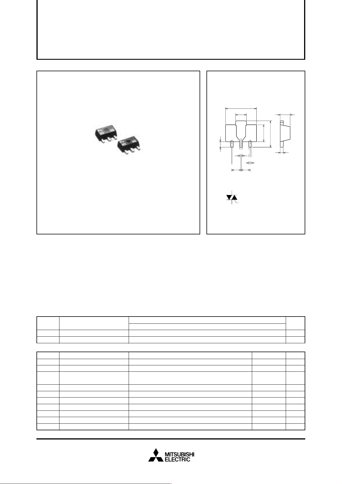
OUTLINE DRAWING
4.4±0.1
1.6±0.2
2
1
0.8 MIN
1.5±0.11.5±0.1
(Back side)
2
1
3
0.5±0.07
0.4±0.07
3
SOT-89
Dimensions
1.5±0.1
2.5±0.1
3.9±0.3
+0.03
0.4
–0.05
T
1
TERMINAL
1
T
2
TERMINAL
2
GATE TERMINAL
3
in mm
APPLICATION
Hybrid IC, solid state relay,
control of household equipment such as electric fan · washing machine,
other general purpose control applications
MAXIMUM RATINGS
Symbol
V
DRM
VDSM
Symbol
T (RMS)
I
ITSM
2
t
I
PGM
PG (AV)
VGM
IGM
Tj
Tstg
—
✽1.Gate open.
Parameter
Repetitive peak off-state voltage
Non-repetitive peak off-state voltage
Parameter
RMS on-state current
Surge on-state current
2
t
for fusing
I
Peak gate power dissipation
Average gate power dissipation
Peak gate voltage
Peak gate current
Junction temperature
Storage temperature
Weight
✽1
✽1
Commercial frequency, sine full wave 360° conduction, T
60Hz sinewave 1 full cycle, peak value, non-repetitive
Value corresponding to 1 cycle of half wave 60Hz, surge on-state
current
Typical value
Voltage class
12 (marked “BF”)
600
720
Conditions
a=40°C
✽3
Ratings
0.8
8
0.26
1
0.1
6
1
–40 ~ +125
–40 ~ +125
48
Unit
V
V
Unit
A
A
2
A
s
W
W
V
A
°C
°C
mg
Mar. 2002

MITSUBISHI SEMICONDUCTOR 〈TRIAC〉
NON-INSULATED TYPE, PLANAR PASSIVATION TYPE
ELECTRICAL CHARACTERISTICS
Symbol
I
DRM
VTM
VFGT !
VRGT !
VRGT #
VFGT #
IFGT !
IRGT !
IRGT #
IFGT #
VGD
Rth (j-a)
(dv/dt)c
✽2.Measurement using the gate trigger characteristics measurement circuit.
✽3.Mounted on 25mm × 25mm × t0.7mm ceramic plate with solder.
✽4.Test conditions of the critical-rate of rise of off-state commutating voltage is shown in the table below.
Repetitive peak off-state current
On-state voltage
Gate trigger voltage
Gate trigger current
Gate non-trigger voltage
Thermal resistance
Critical-rate of rise of off-state
commutating voltage
Parameter
✽2
✽2
T
j=125°C, VDRM applied
c=25°C, ITM=1.2A, Instantaneous measurement
T
!
@
T
j=25°C, VD=6V, RL=6Ω, RG=330Ω
#
$
!
@
T
j=25°C, VD=6V, RL=6Ω, RG=330Ω
#
$
T
j=125°C, VD=1/2VDRM
Junction to case
✽4
Tj=125°C
Test conditions
✽3
BCR08AS
LOW POWER USE
Limits
Typ.
Min.
—
—
—
—
—
—
—
—
—
—
—
—
—
—
—
—
—
—
—
—
—
0.1
—
—
—
0.5
Max.
1.0
2.0
2.0
2.0
2.0
2.0
10
—
65
—
Unit
mA
V
V
V
V
V
5
mA
5
mA
5
mA
mA
V
°C/W
V/µs
Test conditions
1. Junction temperature
T
j=125°C
2. Rate of decay of on-state commutating current
(di/dt)
c=–0.4A/ms
3. Peak off-state voltage
V
D=400V
PERFORMANCE CURVES
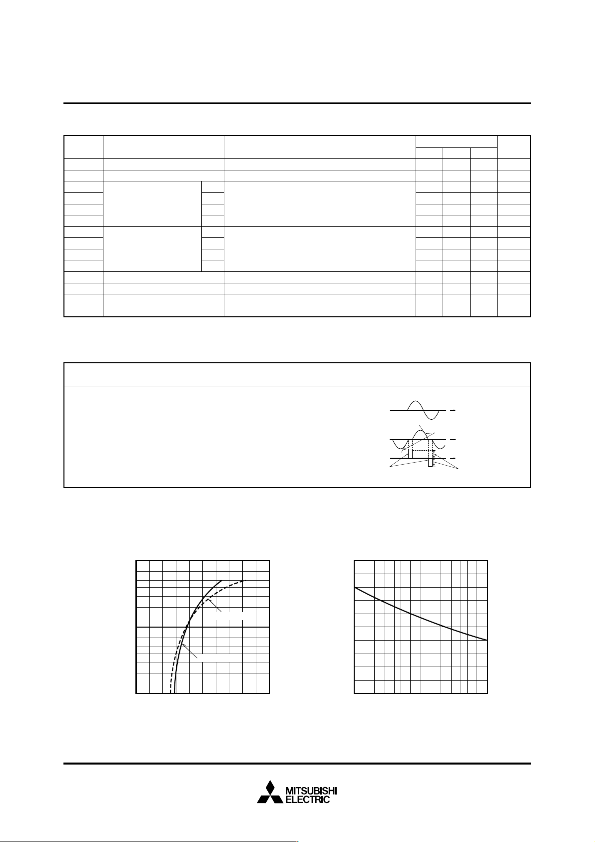
MAXIMUM ON-STATE CHARACTERISTICS
1
10
7
5
4
3
2
0
10
7
5
4
3
ON-STATE CURRENT (A)
2
–1
10
012
Tj = 125°C
Tj = 25°C
345
Commutating voltage and current waveforms
SUPPLY
VOLTAGE TIME
MAIN CURRENT
MAIN
VOLTAGE
(inductive load)
(di/dt)c
(dv/dt)c
RATED SURGE ON-STATE CURRENT
10
8
6
4
2
SURGE ON-STATE CURRENT (A)
0
10023 5710
44
1
23 5710
TIME
TIME
V
D
2
ON-STATE VOLTAGE (V)
CONDUCTION TIME
(CYCLES AT 60Hz)
Mar. 2002

GATE CHARACTERISTICS
2
10
7
5
3
VGM = 10V
2
1
10
7
5
V
GT
3
2
0
10
7
GATE VOLTAGE (V)
5
3
2
–1
10
0
2310
5710123 5710223 5710
I
FGT I
I
RGT I
FGT III
P
G(AV)
= 0.1W
,
, I
RGT III
PGM = 1W
IGM = 1A
VGD = 0.2VI
MITSUBISHI SEMICONDUCTOR 〈TRIAC〉
BCR08AS
LOW POWER USE
NON-INSULATED TYPE, PLANAR PASSIVATION TYPE
GATE TRIGGER CURRENT VS.
JUNCTION TEMPERATURE
3
10
7
100 (%)
5
4
3
2
= t°C)
= 25°C)
j
j
2
10
7
5
4
3
2
1
10
GATE TRIGGER CURRENT (T
3
GATE TRIGGER CURRENT (T
–40 0 40 80 120
–60 –20 20
TYPICAL EXAMPLE
I
FGT III
I
FGT I IRGT III IRGT I
60 100 140
GATE CURRENT (mA)
GATE TRIGGER VOLTAGE VS.
JUNCTION TEMPERATURE
3
100 (%)
)
)
= t°C
= 25°C
j
j
T
T
(
(
10
10
7
5
4
3
2
2
7
5
4
V
RGT I VRGT III
TYPICAL EXAMPLE
V
FGT I VFGT III
3
2
1
10
GATE TRIGGER VOLTAGE
GATE TRIGGER VOLTAGE
–40 0 40 80 120
–60 –20 20
60 100 140
JUNCTION TEMPERATURE (°C)
MAXIMUM ON-STATE POWER
DISSIPATION
2.0
1.6
1.2
0.8
0.4
ON-STATE POWER DISSIPATION (W)
0
0.4 0.8 1.2 1.6
360°
CONDUCTION
RESISTIVE,
INDUCTIVE
LOADS
JUNCTION TEMPERATURE (°C)
MAXIMUM TRANSIENT THERMAL
IMPEDANCE CHARACTERISTICS
TRANSIENT THERMAL IMPEDANCE (°C/W)
10
10
10
10
2
2310
3
7
5
3
2
2
7
5
3
2
1
7
5
3
2
0
5710323 5710423 5710
JUNCTION TO AMBIENT
JUNCTION TO CASE
–1
2310
5710023 5710123 5710
5
2
CONDUCTION TIME
(CYCLES AT 60Hz)
ALLOWABLE CASE TEMPERATURE
VS. RMS ON-STATE CURRENT
160
CURVES APPLY REGARDLESS
OF CONDUCTION ANGLE
140
NATURAL CONVECTION
120
RESISTIVE,
INDUCTIVE
100
LOADS
80
60
40
CASE TEMPERATURE (°C)
20
2.00
0
0.2 0.6 1.0 1.4
0.4 0.8 1.2
1.60
RMS ON-STATE CURRENT (A)
RMS ON-STATE CURRENT (A)
Mar. 2002

REPETITIVE PEAK OFF-STATE
CURRENT VS. JUNCTION
100 (%)
5
10
)
)
= t°C
= 25°C
j
j
T
T
(
(
REPETITIVE PEAK OFF-STATE CURRENT
REPETITIVE PEAK OFF-STATE CURRENT
TYPICAL EXAMPLE
7
5
3
2
4
10
7
5
3
2
3
10
7
5
3
2
2
10
TEMPERATURE
–20 0 20 60 80 100120
JUNCTION TEMPERATURE (°C)
MITSUBISHI SEMICONDUCTOR 〈TRIAC〉
BCR08AS
LOW POWER USE
NON-INSULATED TYPE, PLANAR PASSIVATION TYPE
HOLDING CURRENT VS.
JUNCTION TEMPERATURE
3
10
7
100 (%)
5
3
)
)
(
2
= t°C
= 25°C
j
j
T
T
(
2
10
7
5
3
2
HOLDING CURRENT
HOLDING CURRENT
1
14040–40–60
10
JUNCTION TEMPERATURE (°C)
TYPICAL EXAMPLE
14040–40–60 –20 0 20 60 80 100120
LACHING CURRENT VS.
JUNCTION TEMPERATURE
2
10
7
DISTRIBUTION
5
3
2
1
10
7
5
3
2
0
10
7
5
+
+
T
2
10
, G
3
2
–1
TYPICAL
–
–
T
2
, G
EXAMPLE
–
+
T
2
, G
0 40 80 120
LACHING CURRENT (mA)
JUNCTION TEMPERATURE (°C)
BREAKOVER VOLTAGE VS.
RATE OF RISE OF
OFF-STATE VOLTAGE
160
100 (%)
)
TYPICAL EXAMPLE
140
)
120
100
dv/dt = 1V/µs
dv/dt = xV/µs
80
(
(
60
III QUADRANT
40
20
0
BREAKOVER VOLTAGE
BREAKOVER VOLTAGE
0
5710123 5710223 5710
2310
+
–
T
2
, G
TYPICAL EXAMPLE
Tj = 125°C
I QUADRANT
BREAKOVER VOLTAGE VS.
JUNCTION TEMPERATURE
160
TYPICAL EXAMPLE
140
100 (%)
120
)
)
100
= t°C
= 25°C
j
j
T
T
(
(
80
60
40
20
BREAKOVER VOLTAGE
BREAKOVER VOLTAGE
160–40
0
100120
14040–40–60 –20 0 20 60 80
JUNCTION TEMPERATURE (°C)
COMMUTATION CHARACTERISTICS
1
10
10
7
5
3
2
0
7
TYPICAL
EXAMPLE
j
= 125°C
T
T
= 1A
I
τ = 500µs
D
= 200V
V
f = 3Hz
III QUADRANT
5
MINIMUM
3
CHARAC-
2
10
TERISTICS
VALUE
–1
–1
10
23 5710
COMMUTATING VOLTAGE (V/µs)
3
CRITICAL RATE OF RISE OF OFF-STATE
I QUADRANT
0
23 5710
1
RATE OF RISE OF OFF-STATE VOLTAGE (V/µs)
RATE OF DECAY OF ON-STATE
COMMUTATING CURRENT (A/ms)
Mar. 2002

MITSUBISHI SEMICONDUCTOR 〈TRIAC〉
BCR08AS
LOW POWER USE
NON-INSULATED TYPE, PLANAR PASSIVATION TYPE
GATE TRIGGER CURRENT VS.
GATE CURRENT PULSE WIDTH
3
10
7
5
100 (%)
4
3
)
)
tw
DC
2
(
(
2
10
7
I
RGT I IRGT III IFGT I
5
I
4
FGT III
3
2
GATE TRIGGER CURRENT
GATE TRIGGER CURRENT
1
10
10
0
44
23 5710
GATE CURRENT PULSE WIDTH (µs)
TYPICAL EXAMPLE
1
23 5710
GATE TRIGGER CHARACTERISTICS
TEST CIRCUITS
6Ω 6Ω
6V 6V
A
R
V
G RG
TEST PROCEDURE 1
TEST PROCEDURE 2
A
V
6Ω 6Ω
2
6V 6V
TEST PROCEDURE 3
A
V
RG RG
TEST PROCEDURE 4
A
V
Mar. 2002
 Loading...