POWEREX AY08A3-14, AY08A3-12, AY08A4-8, AY08A4-14, AY08A4-12 Datasheet
...
AY08A3-**
AY08A4-**
Powerex, Inc., 200 Hillis Street, Youngwood, Pennsylvania 15697-1800 (724) 925-7272
916
C
D
E
N∞
81
SEATING PLANE
B
A
M
L
F
J
G
H
K
16-Pin Multiple
Circuit T riac
0.8 Amperes/400-700 Volts
Description:
A triac is a solid state silicon AC
switch which may be gate
triggered from an off-state to an
on-state for either polarity of
applied voltage.
Features:
M Planar Passivation
M Surface Mount Type
M Multiple Circuits in
one Package
Applications:
M Electric Fan
M Air Cleaner
M Small Motor Control
T
16
1
T
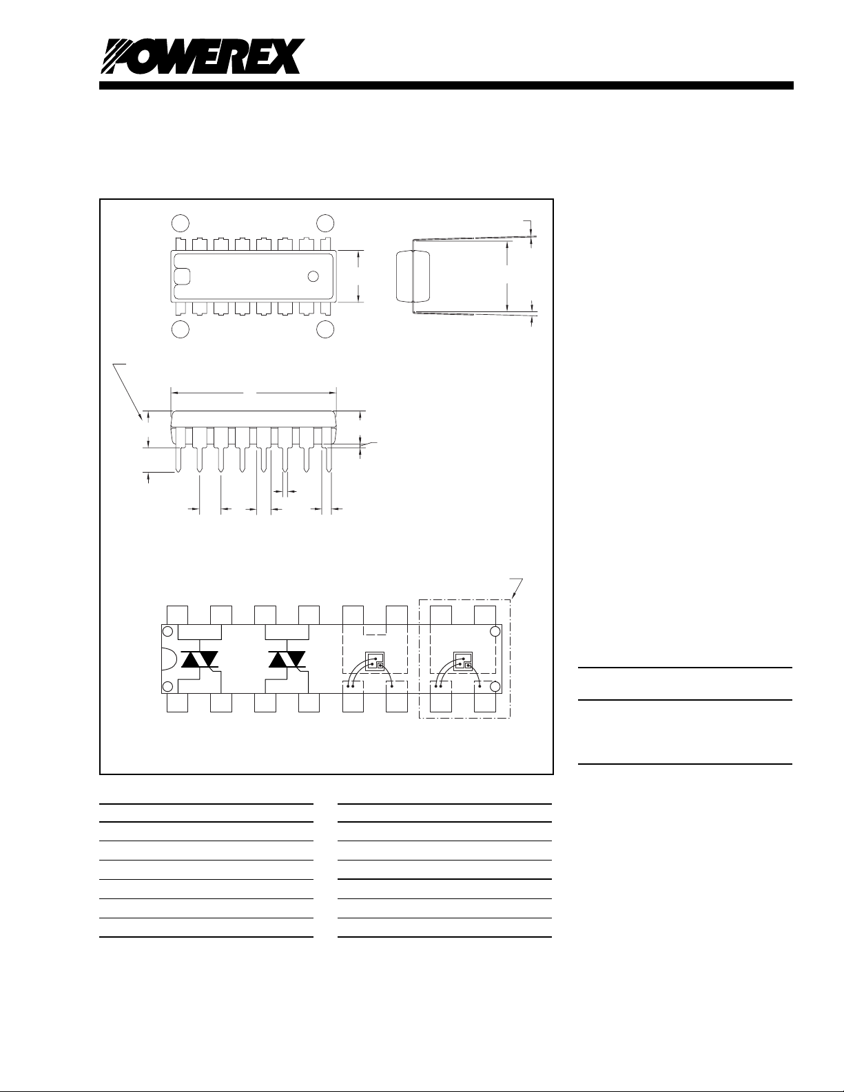
Outline Drawing
Dimension Inches Millimeters
A 1.8 Max. 4.5 Max.
B 0.75±0.01 19.0±0.2
C 0.25±0.01 6.3±0.15
D 0.01 0.27 +0.07/-0.05
E 0.3 7.62
F 0.12 Min. 3.0 Min.
T
2
GT1GT1GT1G
1
T
2
2
AY08A3-**: No chip
T
T
2
Dimension Inches Millimeters
T
2
G 0.1 2.54
H 0.06 +0.01/-0 1.5 +0.3/-0.1
J 0.02 0.5±0.1
K 0.04 +0.01/-0 1.0 +0.3/-0.1
L 0.02 Min. 0.51 Min.
M 0.13 3.3
T
2
2
Ordering Information:
Example: Select the complete
part number from the table
T
2
9
8
below -i.e. AY08A4-14 is a
0.8 Ampere, 4 Circuit, 700V,
16-Pin Multiple Circuit Triac.
Number Voltage
Type of Circuits (x 50)
AY08A 3 -8
4 -12
-14
1

Powerex, Inc., 200 Hillis Street, Youngwood, Pennsylvania 15697-1800 (724) 925-7272
AY08A3-**
AY08A4-**
16-Pin Multiple Circuit Triac
0.8 Amperes/400-700 Volts
Absolute Maximum Ratings (for One Chip), Tj = 25°C unless otherwise specified
Characteristics Symbol AY08A*-08 AY08A*-12 AY08A*-14 Units
Repetitive Peak Off-state Voltage, Gate Open V
Non-Repetitive Peak Off-state Voltage, Gate Open V
On-state Current, Tc = 86°CI
Non-repetitive Peak Surge, One Cycle (60Hz) I
DRM
DSM
T(RMS)
TSM
400 600 700 Volts
500 720 840 Volts
0.8 0.8 0.8 Amperes
8 8 8 Amperes
I2t for Fusing, t = 8.3 msec I2t 0.26 0.26 0.26 A2sec
Peak Gate Power Dissipation, 20 msec P
Average Gate Power Dissipation P
G(avg)
Peak Gate Current I
Peak Gate Voltage V
Storage Temperature T
Operating Temperature T
GM
GM
GM
stg
j
1 1 1 Watts
0.1 0.1 0.1 Watts
0.8 0.8 0.8 Amperes
6 6 6 Volts
-40 to 125 -40 to 125 -40 to 125 °C
-40 to 125 -40 to 125 -40 to 125 °C
Electrical and Thermal Characteristics (for One Chip), Tj = 25°C unless otherwise specified
Characteristics Symbol Test Conditions Min. Typ. Max. Units
Repetitive Off-state Current, Peak I
Peak On-state Voltage V
DRM
TM
Thermal Resistance
Junction to Ambient R
th(j-a)
Gate — Parameters
Gate Current to Trigger II I
Gate Current to Trigger III I
Gate Voltage to Trigger II V
Gate Voltage to Trigger III V
Non-triggering Gate Voltage V
Critical Rate-of-Rise of Commutating (dv/dt)
IT
RGT
III RL = 6V, RG = 330V – – 5.0 mA
RGT
IT
RGT
III RL = 6V, RG = 330V – – 2.0 Volts
RGT
GD
c
Off-state Voltage (dv/dt)c = -0.4A/ms, VD = 400V
V
applied, Tj = 125°C – – 1.0 mA
DRM
Tc = 25°C, ITM = 1.2A – – 2.0 Volts
– – – 120 °C/Watt
= 25°C, VD = 6V – – 5.0 mA
j
= 25°C, VD = 6V – – 2.0 Volts
j
Tj = 125°C, VD = 1/2 V
DRM
0.1 – – Volts
Tj = 125°C 0.5 V/µs
2
 Loading...