

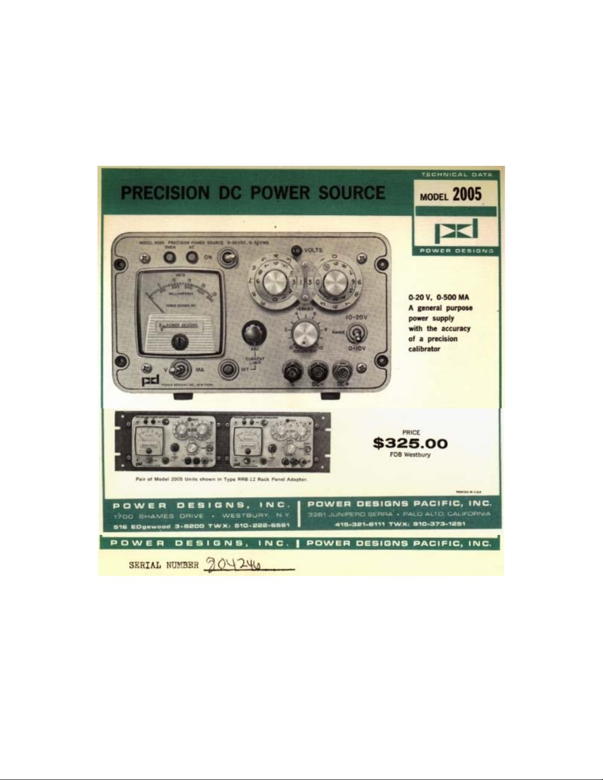
Page 1
Page 2

Description
New high-stability, low-noise silicon semiconductor devices
and advanced solid-state circuit technology are the basis for
this unusually stable voltage regulator. The improved
performance of the Model 2005 permits dial readout of the
output voltage to five places. Interpolation of the last place is
provided by a potentiometer with a resolution of 10 microvolts.
Conventional, more complex chopper techniques for DC
amplifier stabilization are avoided by maintaining critical
amplifier stages and a specially processed zener diode voltage
reference in a temperature-controlled oven. The design
simplicity results in a low-cost unit, half the size and weight of
comparable instrumentation.
Design Features of the Model 2005
• Self-restoring electronic overload and short-circuit
protection.
• All silicon-semiconductor regulator system.
• Critical semiconductors and components maintained
at constant ambient in temperature-controlled oven.
• Accurate remote programming at 1000 ohms-per.volt.
• Front and rear access to output terminals.
• 100 hour pre-aging of power supply before test and
calibration. Individual calibration data furnished with
each unit.
• Line and load circuits separately fused. Accessible at
rear. Performance specifications based on anticipated
ratings after 5 years service.
• "Controlled-Parameter" semiconductor program
• Calibrated decade voltage readout to four significant
figures at outputs below 10 volts, to five significant
figures above 10 volts. Interpolation of the last place
is provided by a potentiometer with 10-microvolts
resolution.
• Provisions for rear-panel zero calibration (may be
used to offset lead drop during remote sensing).
• Adjustable current limiting.
insures long life expectancy. Features "controlled
avalanche" silicon rectifiers and power transistors,
pre-aged zener voltage references and transistors,
noise-testing techniques for establishing predictable
device reliability, derating to 50% of rated voltage and
current, etc.
• Modular package construction suitable for rack
mounting. Single or dual mounting in 5¼"x 19" panel.
See Cat. RPA-62 for rack panel adapters.
General Description
• OUTPUT - 0 to 20 VDC, continuously adjustable, at 0 to 500 MA.
• INPUT - 105 to 125 V, 50 to 440 Hz, 40 W max. (Including oven heater).
• CALIBRATION AND ACCURACY - Two dual, concentric, decade switches provide dial
readout to four places with an accuracy of 0.1% ± 1 MV at outputs below 10 V. A 1-MV
range, single-turn potentiometer permits interpolation of the last place. This potentiometer
has a resolution of 10 uV. A toggle switch extends the range of the dial readout from 10 to
20 V, without affecting resolution or accuracy (five-place readout). An illuminated
indicator identifies the range in operation.
• REGULATION - Output voltage change less than 100 uV (at sense connection points) for
line or load variations over the operating range.
• RIPPLE AND NOISE - Less than 100 uV peak-to-peak.
• SOURCE IMPEDANCE - Less than 0.2 milliohm at DC, 0.04 ohm at 20 KHz, 0.5 ohm at
1 MHz.
• RECOVERY TIME - Less than 10 uS to return to within 250 uV or 0.005% (whichever is
greater) of the set voltage for a 10% to 100% step change in rated load; less than 40 uS to
return with 100 uV.
• OPERATING TEMPERATURE RANGE - 15 to 4 °C ambient; 0 to 60 °C ambient with
reduced accuracy.
• TEMPERATURE COEFFICIENT - DC output voltage change less than 0.001% or 50 uV
(whichever is greater) per °C over the range of +15 to +45°C; less than 0.002% or 100uV
(whichever is greater) per °C from 0 to +15°C and +45 to +60 °C.
i
Page 3

• STABILITY - Better than 0.001% + 100 MV/8 hrs.; better than 1 MV/wk (at constant
ambient temperature, load and line voltage, after warmup).
• OUTPUT TERMINALS - Three front-panel binding posts and rear-panel barrier block.
Either positive or negative output terminal may be grounded.
• METER - Front-panel volt-ammeter permits monitoring output voltage or current with an
accuracy of ±2%.
• REMOTE SENSING - Two terminals on rear-panel barrier block are provided for remote
sensing of voltage at the load.
• REMOTE PROGRAMMING - Rear terminals are provided for remote programming of
the output voltage at 1000 ohms-per-volt. Accuracy of programming is better than 0.01%
of value of resistance (including connecting leads).
• CURRENT LIMITING - The output current can be limited to any value from 0 to 500
MA by a front-panel control. A push-button permits easy adjustment without the need for
shorting the output terminals.
ii
Page 4
SECTION 1
GENERAL DESCRIPTION
1-1. DESCRIPTION
The Model 2005 is a precision DC power source designed to supply an extremely stable 0 to 20 volt, 0 to
500 milliampere output. The instrument combines the accuracy of a precision calibrator with the power
capability of a general-purpose regulated supply. Two dual, concentric decade switches provide a digital
readout of the selected output voltage to within 0.1% +1 millivolt of the selected value. A 1-millivolt
range, single-turn potentiometer permits interpolation of the last place. This potentiometer has a
resolution of 10 microvolts. A toggle switch selects the range of the dial readout; either from 0 to 10
volts, or from 10 to 20 volts. The output voltage of the supply may be remotely programmed with the
same accuracy, using an external resistance. The supply also includes provisions for remote sensing of the
output voltage at the load. Compact and light, the power source is self-contained in a portable housing
designed for bench use. The modular construction of the Model 2005 makes it suitable for rack mounting.
Panel adapters are available for mounting one or two units in a standard 19-inch rack having a panel
height of 5 1/4 inches.
1-2. ELECTRICAL SPECIFICATIONS
Refer to Table 1 for a complete list of electrical specifications.
TABLE 1. ELECTRICAL SPECIFICATIONS
Parameter Value
Output 0 to 20 volts DC, continuously adjustable, 0 to 500 milliamperes
105 to 125 volts, 50 to 440 Hz, 40 watts (nominal) Regulation DC voltage change less
Input
Ripple and
Noise
Source
Impedance
Recovery Time
Stability
Temperature
Coefficient
Calibration
Accuracy
than 100 microvolts for line variations of ±10% or load variations of 100% (at sense
lead connection points)
Less than 100 microvolts peak-to-peak
Less than 0.2 milliohm at DC, 0.04 ohm at 20 KHz, 0.5 ohm at 1 MHz
Less than 10 microseconds to return to within 250 microvolts or 0.005% (whichever is
greater) of the set voltage for a step change in rated load (1 microsecond rise time) of
10% to 100% or 100% to 10%; less than 40 microseconds to return to within 100
microvolts
Better than 0.001% +100 microvolts per 8 hours; better than 1 millivolt per week (at
constant line, load and ambient temperature after warm-up).
DC output voltage change less than 0.001% or 50 microvolts (whichever is greater) per
°C over the range of +15 °C to +45 °C, less than 0.002% or 100 microvolts (whichever
is greater) per0 °C from °C from 0 °C to +15°C and from +45 °C to +60 °C
Better than 0.1% +1 millivolt
Current
Limiting
0 to 500 milliamperes continuously adjustable by a front panel control. A front panel
push button permits easy adjustment without shorting the output terminals.
1‐1
Page 5
Output Terminals
Front Panel Three insulated binding posts for positive output, negative output, and chassis ground
Rear Panel
Remote Sensing
Screw terminals on a molded barrier block for positive output, negative output, chassis
ground, remote voltage programming and remote sensing.
Two terminals are provided on a rear panel barrier block for remote sensing of the
voltage at the load.
Parameter Specifications
Rear panel barrier block terminals are provided for remote programming of the output
Remote
Programming
voltage. The ratio of the programming resistance to the output voltage is 1000 ohms
per volt. The programming accuracy is better than 0.01% of the resistance value,
including the resistance of the programming leads.
Front panel volt-ammeter permits monitoring output voltage or current with an
Metering
accuracy of ±2% of full scale.NOTE: This accuracy is considerably less than that of the
power source.
Circuit
Protection
The AC line and DC load circuits are separately fused. The fuses are accessible at the
rear of the unit.
Indicator Lamps
AC Lamp Lights when AC toggle switch is set to ON and power is applied to the unit.
Lights when AC input is applied and oven heater is energized (operates even when AC
OVEN Lamp
toggle switch is turned off). Lamp cycles on and off as oven maintains constant
temperature environment for critical components.
+10 V Lamp
Lights when RANGE switch is set to 1O-20V position to indicate that output is 10
volts plus the dial readout.
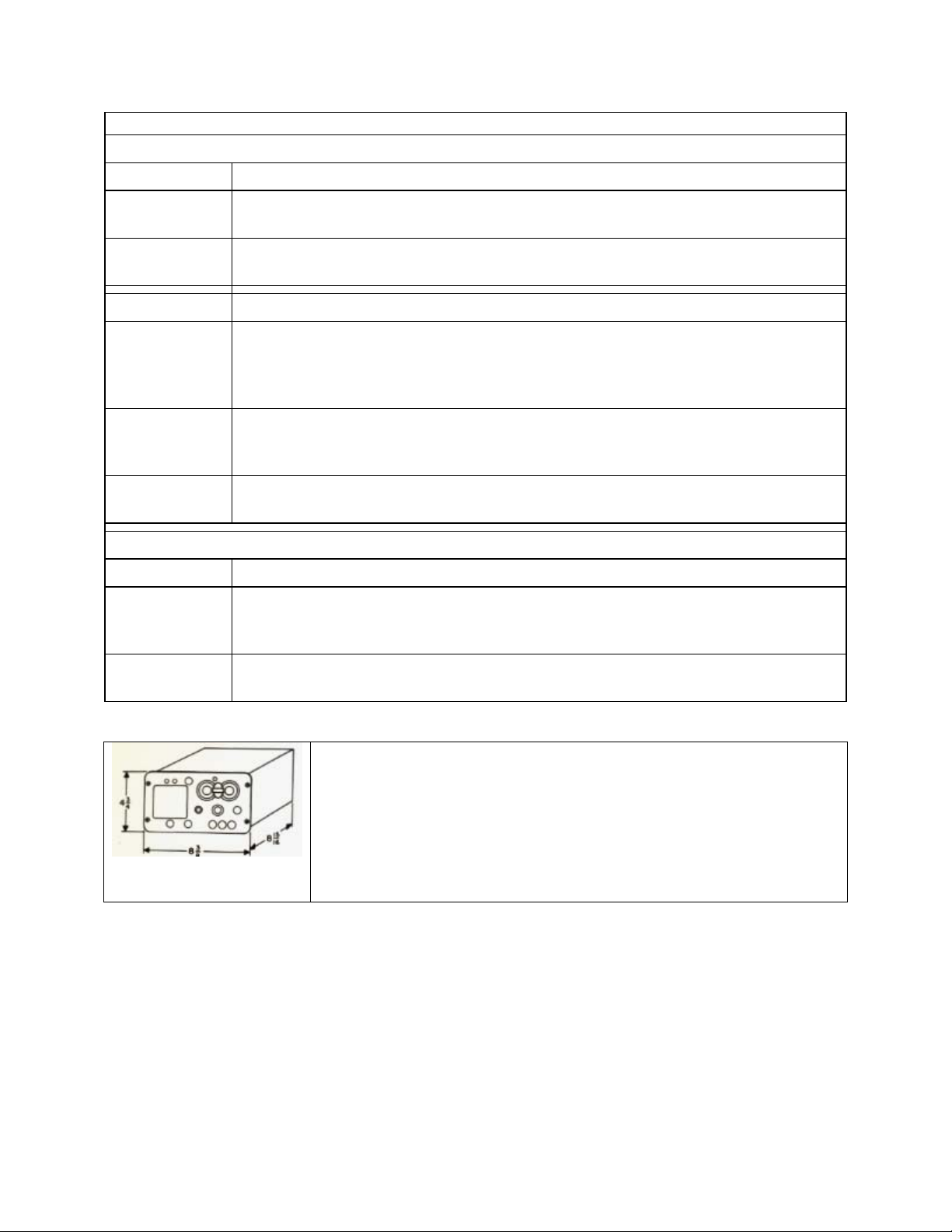
1-3. MECHANICAL SPECIFICATIONS
• Dimensions : 8-3/8 inches wide by 4-3/4 inches high by 8-
• Weight : 9 pounds.
• Finish : The panel is finished in brushed aluminum and has
15/16 inches deep behind the front panel.
etched black lettering. The housing is finished in blue-gray
vinyl enamel. The chassis and bottom plate are gold iridite.
1‐2
Page 6

SECTION 2
2) INSTALLATION AND OPERATION
2-1 INSTALLATION
a) Laboratory Bench . The Model 2005 is a portable unit designed for bench use. No
preliminary processing or special unpacking procedures are required. The power source is
ready for operation as shipped from the factory.
b) Rack Mounting . Panel adapters are available for mounting one or two units in a standard 19-
inch relay rack. Hardware kits are provided with each panel adapter. The power source is
fastened to the rear surface of the adapter with the black anodized rivnuts in each corner of its
front panel. If the rubber bumper feet interfere with the assembly of the equipment to the
rack, they may be removed by disassembling the bottom plate of the power source and
unscrewing them.
2-2 OPERATION
a) Operating Procedures:
(i) Ensure that the power source is turned off and the shorting links are connected between
the following rear-panel terminals: DC+ and S+; S+ and RV; and S- and DC-.
(ii) Set the CURRENT LIMIT ADJ control fully clockwise.
(iii) Connect the AC line cord to a source of 105 to 125 volts, 50 to 440 Hz. NOTE: The
OVEN indicator will normally light as soon as line voltage is applied to the unit, even
when the power source is turned off. The indicator will remain lighted until the oven
reaches operating temperature (approximately 10 minutes). The indicator will cycle on
and off as the oven maintains a constant- temperature environment for critical circuit
components.
(iv) Read the information in paragraphs b through e to connect for remote sensing, series
operation, remote programming of the output voltage, or current limiting.
(v) Set the AC switch to ON.
(vi) Set the output voltage to the desired value, using the front panel dials. Set the
VERNIER control to zero if interpolation between 1 millivolt steps is not desired.
(vii) Connect the DC+ and DC- terminals (on the front or rear panel) across the load. If
desired, connect the positive or negative output terminal to ground.
b) Sensing: The regulator circuit maintains the potential between the sense leads (s+ and S-) at
the set output voltage. When these leads are connected to the positive and negative output
terminals, the power source is connected for local sensing. When the sense leads are
connected to the load, the source is connected for remote sensing. Remote sensing is used
when an appreciable voltage drop is anticipated in the leads connecting the positive and
negative output terminals to the load. The Model 2005 is connected for local sensing when
shipped from the factory. For remote sensing, proceed as follows:
(i) Remove the shorting links from between the rear panel DC+ and S+ terminals and from
between the DC- and S- terminals.
(ii) Connect the DC+ and DC- leads across the load.
(iii) Connect the S+ and S- leads to the positive and negative sides of the load, respectively.
Run the sense leads as a tightly twisted, shielded pair. Connect the shield to the G
(chassis ground) terminal to minimize output ripple
(iv) Turn on the Model 2005.
2‐1
Page 7

c) Series Operation: As many as four Model 2005 units may be connected in series to provide
up to 80 volts. Connect the positive DC output terminal of one supply to the negative output
terminal of the next, in the same manner as connecting batteries in series. The ground
terminals on all units may be left floating or they may be tied together and connected to either
the most positive or the most negative output terminal. To insure optimum voltage regulation,
disconnect the shorting links between all S+ and DC+ output terminals except those at the
most positive potential. Then connect jumper wires between each S+ terminal and the Sterminal on the next more positive power source. In this way, the voltage drops in the leads
connecting the power sources will be compensated for by the regulator circuits of the
individual units. For remote sensing, proceed as directed above, except connect the most
positive and most negative S+ and S- leads across the load.
d) Remote Voltage Programming: The output voltage can be programmed remotely by an
external fixed or variable resistance. Proceed as follows:
(i) Turn off the power source, set all output voltage controls to zero and set the RANGE
switch to 0 -10V.
(ii) Remove the shorting link from between the rear panel RV and S+ terminals.
(iii) Select a programming resistance by multiplying the desired output voltage by 1000 (the
programming constant is 1000 ohms per volt). A constant current of 1 milliampere will
flow through this resistance, and its wattage rating should be chosen to minimize drift
due to heating.
(iv) Connect the external programming resistance between the RV and S+ terminals using
twisted, shielded wire. Connect the shield to the G (chassis ground) terminal to minimize
output ripple.
(v) Turn on the power source.
CAUTION: IF THE REMOTE PROGRAMMING CONNECTIONS ARE OPENED
WHILE THE SUPPLY IS OPERATING, THE OUTPUT VOLTAGE WILL RISE
SLIGHTLY ABOVE THE SET VALUE. WHEN A SWITCH IS USED TO SELECT
RESISTORS FOR OUTPUT VOLTAGE PROGRAMMING, IT SHOULD HAVE
SHORTING TYPE CONTACTS TO AVOID VOLTAGE SPINES.
e) Current Limiting: The maximum output may be limited to a value below 500 milliamperes as
follows:
(i) Turn on the power source and set the meter switch to MA.
(ii) Depress the CURRENT LIMIT SET button and adjust the CURRENT LIMIT ADJ
control until the meter indicates the maximum desired output current. Release the
CURRENT LIMIT SET button.
2‐2
Page 8

SECTION 3
3) PRINCIPLES OF OPERATION
3-1 GENERAL
The Model 2005 is a highly accurate, series regulated, DC voltage source. Basically, it consists of
a full-wave rectifier circuit, a series regulator circuit and a current limiting circuit.
The series regulator circuit is essentially an electronically variable resistance interposed between
the unregulated source and the load. The resistance value is controlled by an amplifier that
compares the source output voltage with a reference voltage. The amplifier adjusts the series
resistance to reduce the error signal to zero.
The reference voltage is generated by an internal auxiliary power source. The error signal
resulting from the voltage comparison is amplified and applied through a driver stage to the series
transistor to vary its effective resistance.
3-2 FULL-WAVE RECTIFIER OPERATION
The full-wave rectifier consists of diodes CR1 and CR2. Its output is applied through fuse F2
to series regulator transistor Q1. The output of the full-wave rectifier is filtered by capacitor
C1.
3-3 SERIES REGULATOR OPERATION
The series regulator circuit consists of differential amplifier Q5, amplifiers Q4, Q6 and Q7; driver
Q2 and series regulator Q1. The voltage reference for the differential amplifier is zener diode
CR13. A constant current is maintained through CR13 by transistors Q9 and Q10 and zener diode
CR11. These components are powered by an auxiliary 20-volt supply.
The constant voltage across CR13 is impressed across the base- emitter junction of one-half of
Q5. Potentiometer R12 is adjusted to bias the base-emitter junction of the input half of Q5 to the
same potential. Zener diode CR10 provides a constant collector voltage for the input section of
the differential amplifier. A constant current for this zener diode is provided by CR22 and Q10,
which are powered by an auxiliary 20-volt supply.
The differential amplifier, its voltage reference and the transistors that maintain a constant current
through the voltage reference are located on oven board assembly A1. The oven maintains these
components in a constant-temperature environment to provide highly stable operation.
The input to the differential amplifier is applied from a voltage divider across the supply output.
Any change in output voltage changes the bias on the differential amplifier and, consequently,
changes the collector current on the output half of this stage. This changes the drive on amplifiers
Q4, Q6, and. Q7. The changed output of Q7 changes the drive of Q2, and therefore of series
regulator Q1. This change in drive on Q1 is in the correct direction to oppose any change in the
supply output voltage.
3‐1
Page 9

For example, if the output voltage tends to increase, the forward bias on the input stage of the
differential amplifier increases. This reduces the collector current of the output half of this stage,
reducing the drive of amplifiers Q4, Q6, and Q7. The reduced collector current of Q7 lowers the
forward bias of driver Q2. The reduced collector current of Q2 reduces the forward bias of series
regulator Q1, increasing its effective resistance. The increased resistance of Q1 increases the
voltage drop across it, reducing the output voltage.
3-4 CURRENT-LIMITING CIRCUIT
The current-limiting circuit consists of transistor Q8, diode CR18, and their associated
components. This stage is connected across the auxiliary 20-volt supply. The current through
resistors R21 and R25 through R27 sets the normal bias on this stage. Potentiometer R27 sets the
range of CURRENT LIMIT ADJ R25. This potentiometer is adjusted to forward bias transistor
Q8 at the current-limiting point.
When the output load demand exceeds the value set by potentiometer R25, transistor Q8 conducts
heavily. The collector current of Q8, flowing through R29, forward biases diode CR18. When
diode CR18 conducts, it reduces the forward bias of amplifier Q4. This reduces the drive of the
series regulator transistor, lowering the output voltage.
Any further increase in load demand further reduces the bias on Q4, further reducing the output
voltage. In this manner, the circuit will maintain the load current at the set value for loads down
to a short circuit. When the output current demand is reduced, the circuit conditions reverse and
the voltage regulating circuits regain control of the output.
3‐2
Page 10

SECTION 4
4) MAINTENANCE
4-1 GENERAL
Under normal conditions, no special maintenance of the Model 2005 is required. If servicing is
necessary, the information in this section should be read thoroughly before starting repair or
calibration.
4-2 ADJUSTMENT AND CALIBRATION
Make the following adjustments whenever a component is replaced or periodic recalibration is
scheduled:
a) Preliminary Meter Adjustment:
(i) Mechanically zero the meter using the adjustment screw on the front panel.
(ii) NOTE: Before completing any meter adjustment, lightly tap the meter face. This will
overcome any pivot friction and insure proper calibration.
(iii) Set the CURRENT LIMIT ADJ control fully clockwise.
(iv) Connect a 40-ohm, 10-watt resistor, in series with a standard a mmeter, across the
output of the supply.
(v) Set the AC switch to ON and adjust the output voltage controls for a convenient
reading, approximately ampere on a standard ammeter.
(vi) Set the meter switch to MA.
(vii) Adjust potentiometer R42 (on the board behind the meter) until the panel meter reading
agrees with that of the standard ammeter.
b) Zero Voltage Calibration:
(i) Connect a high precision voltmeter across the output of the supply.
(ii) Set the RANGE switch to the 0-10V position and the output voltage controls for 0.000
volt output.
(iii) Set the AC switch to ON and observe the voltmeter. If the voltmeter does not indicate
0.000 volt ±1 MV, adjust CALIBRATE potentiometer R39 (on the rear panel) for this
reading. If the adjustment is beyond the range of R39, proceed as follows:
(a) Set CALIBRATE potentiometer R39 to the middle of its range.
(b) Disconnect any jumper wires connected across resistors R9, R13, R40 and/or
R41.
(c) Connect jumper wires, in various combinations, across resistors R9, R13, R40,
and R41 until the output is within 2.5 MV of zero. Solder the jumper wires in these
positions.
(d) Adjust CALIBRATE potentiometer R39 for an output of 0.000 volt ±1 MV.
c) 20-Volt Adjustment:
NOTE: Make this adjustment only after the zero voltage calibration.
(i) Set the RANGE switch to 10-20V and adjust the supply output to 20.000 volts. Set the
VERNIER control fully counterclockwise.
(ii) Check that the dots on the VERNIER control and front panel are aligned. A setscrew is
located in the VERNIER control for any necessary adjustment.
(iii) Set the VERNIER control to 0.
(iv)
Connect a high precision voltmeter across the output of the supply.
(v) Set the AC switch to ON and observe the voltmeter.
4‐1
Page 11

(vi) If necessary, adjust potentiometer R12 (on the amplifier board) until the voltmeter
reads 20.000 ±0.007 volts.
d) CURRENT LIMIT ADJ Range Adjustment:
(i) Set the power supply output voltage to 20.000 volts.
(ii) Set the meter switch to MA.
(iii) Set potentiometer R27 (on the amplifier board) to the center of its range.
(iv) Adjust CURRENT LIMIT ADJ potentiometer R25 through its entire range while
depressing CURRENT LIMIT SET push-button S3.
(v) Adjust potentiometer R27 until the CURRENT LIMIT ADJ potentiometer varies the
output current from 0 to 500 MA over its entire range.
(vi) Set the CURRENT LIMIT ADJ potentiometer to the desired maximum output current,
or set it fully clockwise/
4-3 TROUBLE SYMPTOMS AND SUGGESTED REMEDIES
a) Circuit faults can be isolated most rapidly by measuring the voltage and resistance. Use the
data given on the schematic diagram in the Appendix as a first stop in servicing the supply.
CAUTION: WHEN UNSOLDERING SEMICONDUCTORS FOR TEST, USE A HEAT
SINK TO PREVENT THERMAL DAMAGE. A LONG NOSE PLIERS BETWEEN THE
SEMICONDUCTOR AND THE SOLDER JUNCTION IS ADEQUATE. NEVER
OPERATE THE POWER SUPPLY WITH ANY LEADS DISCONNECTED OR
SEMICONDUCTORS REMOVED. OPERATING POTENTIALS IN THE DC AMPLIFIER
MAY CHANGE RADICALLY WHEN A COMPONENT IS REMOVED OR
DISCONNECTED.
b) Power Supply Does Not Go On : If the OVEN and AC lamps do not light, check the AC fuse.
If the fuse blows repeatedly, check the oven circuit and diodes CR1, CR2 and CR4 through
CR7. Use an ohmmeter to take a resistance reading across each diode. Then, reverse the
meter leads and take another reading. If one reading is not at least five times greater than the
other, the diode is defective. If one diode in any pair is defective, replace both. A short circuit
in one will produce high surge currents in the other, which can result in junction damage.
c) No DC Output Voltage: If both the AC and OVEN lamps light, but no output voltage is
available, insure that the CURRENT LIMIT ADJ control is not turned fully
counterclockwise. Set the meter switch to MA and increase the output voltage. If no current is
indicated, check the DC fuse and input capacitor C1. If current is present when the outputvoltage controls are adjusted, check safety diode CR12 and for incorrect programming or
sensing connections. Diode CR12 is connected in the opposite polarity to the DC output
voltage. If the reverse current flow is greater than 1 ampere, this diode may weld, placing a
permanent short circuit across the supply output. Normal operation can be restored by
replacing the diode (located on the amplifier board).
d) Regulator Failure : Check for correct potentials on amplifier transistors, voltage reference,
etc. If any voltage appears incorrect, disconnect AC power and make a rapid check for
defective transistors. This can be done without removing the transistors from the circuit. Use
an ohmmeter sot to its low resistance scale (R x1), and measure the forward and reverse
resistances at the collector-base and base-emitter junctions. A resistance ratio of less than 5 to
1 indicates that the transistor is defective. Carefully remove it and check it on a transistor
checker.
CAUTION: THIS TEST IS NOT RECOMMENDED FOR HIGH FREQUENCY OR LOW
CURRENT DEVICES IN OTHER INSTRUMENTATI0N, AS CURRENTS FROM S0ME
OHMMETERS MAY BE SUFFICIENT TO DAMAGE SMALL SEMICONDUCTOR
JUNCTIONS.
e) To test a component located in the oven:
(i) Unplug the line cord and remove the cover from the power supply.
4‐2
Page 12

(ii) Loosen the three screws that secure the oven cover.
(iii) Rotate the cover counterclockwise and pull it away from the oven.
(iv) Remove the two screws that secure the oven cap; then remove the cap.
(v) Reach into the oven and extract the oven board. NOTE: To test the oven board while
the unit is operating, remove it from its socket and insert a test adapter (Vector Electronic
Corp. Type P-9-N-S, or equal) in its place. The board can then be plugged into the
adapter.
(vi) To reassembl e the oven, replace the board and cap. Secure the cap in position with two
screws. Slide the oven cover down until the screws slide into the slots in the cover. Turn
the cover clockwise and tighten the three screws.
f) Poor Regulation, High Ripple: No specific check can be suggested since failure to regulate
within specifications may be caused by any of the components in the supply. Make a pointto-point voltage and resistance chock. Check all capacitors for open circuits and all
electrolytic capacitors for excessive leakage. Make stage-gain measurements by changing the
output load current and noting the change in base current of each amplifier stage. Use low
resistance milliammeters and microammeters to avoid upsetting the regulator. The open-loop
current gain of the regulator should be more than 106 from the base current of the input
differential amplifier to the collector current of the series regulator.
4‐3
Page 13

APPENDIX
INTRODUCTION
This appendix contains an electrical parts list, schematic diagram, parts location diagram and equipment
warranty.
ELECTRICAL PARTS LIST
All electrical and electronic parts are listed in the sequence of their circuit numbers as shown on the
schematic diagram. A brief description of each part is given, followed by the code number of the
manufacturer and his part number. All manufacturers' code numbers are taken from Cataloging
Handbooks H4-1 and H4-2, Federal Supply Code for Manufacturers. These handbooks are available
through Federal Agencies. They may also be ordered directly from the Superintendent of Documents, U.
S. Government Printing Office, Washington, D.C. 20402.
We recommend that all parts having the code number 98095 be ordered directly from Power Designs Inc.
The commercial equivalents of these parts either have wide parameter tolerances or require special
factory inspection or modification before they are suitable for use in the power supply.
All components used in the power supply or supplied as replacements are carefully inspected at the
factory. Inspections are performed on a 100% basis or at AQL levels in accordance with Military
Specification MIL-Q-9858 under which Power Designs Inc. has been qualified.
All semiconductors are inspected on a 100% basis. They are inspected not only for operating parameters,
but also for critical characteristics related to reliability and predictable life expectancy. Some of those
characteristics are observed when the device is taken beyond its normal operating regions. These test
techniques have been developed under a "predictable-reliability" program in operation at Power Designs
Inc. for the past ten years. Under this program, quality- control procedures arc constantly revaluated and
updated as new advances are made in solid-state technology and additional experience is gleaned from
field history.
Semiconductor manufacturers are constantly modifying their products. Complete lines are frequently
discontinued and replaced by devices having improved gain, operating voltage levels and frequency
response. The high-gain, closed-loop DC amplifiers used in regulator circuits are particularly sensitive to
slight changes in these parameters. Commercial or military "equivalent" transistors used as replacements
may affect the power supply performance. Compliance with the original specifications can be assured if
replacement semiconductors are ordered from the factory.
All replacement semiconductors are processed and stocked at the factory to insure complete
interchangeability with the devices in the original equipment. To insure that proper replacements are
provided, the original devices are coded with a Power Designs Inc. part number as follows:
Semiconductor Manufacturer' s Code Power Designs Inc. Type Suffix Identifying Special Parameters
5‐1
Page 14

When ordering replacements, please identify the device as completely as possible, listing the model and
serial number if available.
In some cases, the replacement part received may have a different part number from that given in the
Electrical Parts List. This can be due to several factors:
• A different prefix indicates that Power Designs Inc. is using a different vendor source. The
operating characteristics of the devices are identical.
• A completely different part number indicates:
• The original vendor discontinued manufacture of the item or could no longer manufacture it
to the original specifications
• A better device for use in the particular circuit has been substituted.
• Tighter controls for interchangeability have provided greater assurance of
5‐2
Page 15

ADDENDA
The Schematic Diagram and Electrical Parts List have been modified as follows:
1. Capacitor C21 has been added directly across CR9 on the auxiliary board. This capacitor is
tantalum, 10 uf, 35 vdc, part number CE-106-.35 (manufacturer 98095).
2. Capacitor C22 has been added across diode CR14. This is plastic film, 0.01 uf, 200 vdc, part
number CP-16-2 (manufacturer 98095).
6‐1
Page 16

ELECTRICAL PARTS LIST
NOTE: When replacing semiconductors or investigating their part numbers, note the information in
paragraph 2 above.
ELECTRICAL PARTS LIST
Circuit
Number
C1 Capacitor,electrolytic,1000 uf, 50 vdc 98095 CE-94-.5
C2,C3 Capacitor,electrolytic,100 uf, 80 vdc 98095 CE-91-.8
C4 Capacitor,electrolytic,8 uf,100 vdc 98095 CE-42-1
C5 Capacitor,electrolytic,400 uf, 85 vdc 98095 CE-83-.85
C6 Capacitor, ceramic disc,0.02 uf, 500 vdc 98095 CC-23-5
C7 Capacitor,electrolytic,100 uf,80 vdc 98095 CE-91-.8
C8 Capacitor, plastic film,0.1 uf, 200 vdc 98095 CP-17-2
Description
Mfr Code
Number
Part Number
C9 Capacitor, ceramic disc,0.05 uf, 600 vdc 98095 CC-34-6
C10,C11 Capacitor, plastic film,0.1 uf, 200 vdc 98095 CP-17-2
C12 Capacitor, ceramic disc,0.01 uf, 1 kvdc 98095 CC-13-10
C13 Capacitor, plastic film,680 pf, 200 vdc 98095 CP-27-2
C14 Capacitor, ceramic disc,O.O1 uf, 1 kvdc 98095 CC-13-10
C15 Capacitor, ceramic tubular,330 pf, 500 vdc 98095 CC-26-5
C16,C17 Capacitor, ceramic disc,1 uf, 3 vdc 98095
C20,C21 Capacitor,tantalum,10 uf, 35 vdc 98095 CE-106-.35
CR1 thru
CR7
CR8, CR9 Diode, silicon, zener 98095 UZ587
CR10,
CR11
CR12 Diode, silicon 98095 GI44
CR13 Diode, silicon, zener (See Note 1) 98095 AC359BT
CR14 thru
CR21
Diode, silicon 98095 G144
Diode, silicon, zener 98095 AC359C, D
Diode, silicon 98095 GI44
CC100M3AD
CR22 Diode, silicon, zener 98095 AC359C,D
F1 Fuse, "Slo-Blo," 3/8 ampere 71400 MDL3/8
F2 Fuse, "Slo-Blo," 1 ampere 71400 MDL 1
I1, I2 Lamp assembly, neon 98095 PLA-7
7‐1
Page 17

Circuit
Number
I3 Lamp assembly, neon 98095 PLA-10
M1 Meter, volt-ammeter, 0-25 V, 0-500 MA 98095 MVA-109
Q1 Transistor, silicon, NPN 98095 RC1700
Q2 Transistor, silicon, PNP 98095 MS1028A
Q3 Transistor, silicon, NPN 98095 MS2270/U
Q4 Transistor, silicon, PNP 98095 MS1028L
Q5 Transistor, dual, silicon,NPN(See Note1) 98095 AS2056
Q6 thru Q8 Transistor, silicon, NPN 98095 MS2270/U
Q9, Q10 Transistor, silicon, PNP 98095 MS1028A
R1 Resistor,wirewound,1 k ohm, 5%, 5 w 98095
R2 Resistor,wirewound,800 ohms,5%, 5 w 98095
R3 Resistor,composition,390 ohms,5%,1/2 w 01121 EB3915
R4 Resistor, precision, metal film,150 k ohms,1%,* w 98095 RD-154-1QA
R5
Description
Resistor, composition, 6.8 megohms to 15 megohms,
10%,1/2 w (precise value selected on test)
Mfr Code
Number
01121 Type EB
Part Number
RW-1023DA
RW-8013DA
R6 Resistor, precision, metal filrn,562 ohms,1%,* w 98095
R7 Resistor, composition, 4.7 k ohms,10%,1/2 w 01121 E34721
R8 Resistor, precision, metal film, 22.1 k ohms,1%,1/4 w 98095
R9 Resistor, precision, metal film, 16.2 k ohms,1%,1/4 w 98095
R10 Resistor, precision, metal film, 35.7k ohms,1%,1/4w 98095
R11 Resistor, precision, wirewound, 5.2k ohms,1%,1/4w 98095
R12 Resistor, variable, wirewound, 200 ohms,10%,3w 98095
R13 Resistor, precision, metal film, 8.25k ohms,1%,1/4w 98095
R15 Resistor, composition, 1.8k ohms,5%,1/2 w 1121 EB1825
R16 Resistor, composition, 560 ohms,10%,1/2 w 1121 EB5611
R17 Resistor, composition, 4.7k ohms,10%,1/2 w 1121 EB4721
R18 Resistor, composition, i.8k ohms,10%,1/2 w 1121 EB1821
RD-56201QA
RD-22121QA
RD-16221QA
RD-35721QA
RW-5228QA
RWV201K4-.68
RD-82511QA
R19 Resistor, composition, 560 ohms,10%,1/2 w 1121 EB5611
7‐2
Page 18

Circuit
Number
R20 Resistor, composition, 100 ohms,10%,1/2 w 1121 EB1011
R21 Resistor, wirewound, 2 ohms,5%, 5 w 98095
R22 Resistor, precision, metal film, 475 ohms,1%,1/4w 98095
R23 Resistor, precision, metal film, 150 ohms,1%,1/4w 98095 RD-151-1QA
R24 Resistor, composition, 5.6 k ohms,10%,1/2 w 1121 EB5621
R25 Resistor, variable, wirewound, 1 k ohm,10%, 2 w 98095
R26 Resistor, composition, 4.7 k ohms,10%,1/2 w 1121 EB4721
R27 Resistor, variable, wirewound, i k ohm, 10%,1 1/4w 98095 RWT-102-C4
R28 Resistor,composition,3.9 k ohms, 10%,2 w 1121 HB3921
R29 Resistor,composition,22 k ohms, 5%,1/2 w 1121 EB2235
R30 Resistor,composition,2.7 k ohms, 10%,1/2 w 1121 EB2721
R31 Resistor, wirewound, 500 ohrns, 5%,5 w 98095
Description
Mfr Code
Number
Part Number
RW-0203DA
RD-47501QA
RWV102C4-.78
RW-5013DA
R32 Resistor,composition,560 ohms, 10%,1/2 w 1121 EB5611
R33 Resistor, precision, wirewound, 24.9k ohms,O.5%,*w 98095
R37,R38 Resistor, precision, metal film, 221 ohms,1%,1/4w 98095
R39 Resistor, variable, wirewound, 5 k ohms,10%,4 w 98095
R40 Resistor, precision, metal film, 4.32 k ohms,1%,1/4w 98095
R41 Resistor, precision, metal film, 32.4 k ohms,1%,1/4w 98095
R42 Resistor, variable, wirewound, 50 ohms,10%,1 1/4w 98095 RWT-500-C4
R43 Resistor, wirewound, 0.2 ohm shunt 98095 RW-FA-4A
R45 Resistor, precision, wirewound, 10 k ohms,0.1%,0.4w 98095
R46 Resistor, variable, wirewound, 1 ohm,10%,2 w 98095
R47 Resistor, precision, wirewound, 1 k ohm, 0.1%, 0.4w 98095 RW-l02-8UR
R48,R49 Resistor, precision, wirewound, 2 k ohms,0.1%,0.4w 98095
RW-24926QA
RD-22101QA
RWV502M4-.87
RD-43211QA
RD-32421QA
RW-1038UR
RWV010C4-.81
RW-2028UR
R50 Resistor, precision, wirewound, 5 k ohms,0.1%,0.4w 98095
RW-5028UR
7‐3
Page 19

Circuit
Number
R51 Resistor,composition,4.7 k obms,10%, 1/4 w 1121 CB4721
R52 Resistor,composition,6.8 k ohms,10%, 1/4 w 1121 CB6821
R53 Resistor,composition,18 k ohms,10%, 1/4 w 1121 CB1831
R54 Resistor,composition,27 k ohms,10%, 1/4w 1121 CB2731
R55 Resistor,precision,wirewound,100 ohms, 0.1%,0.4w 98095
R56,R57 Resistor, precision, wirewound, 200 ohms,0.1%,0.4w 98095
R58 Resistor, precision, wirewound, 500 ohms, 0.1%,0.4w 98095
R59 Resistor, composition, 470 ohms, 10%,1/4 w 1121 CB4711
R60 Resistor, composition, 680 ohms,1 0%,1/4 w 1121 CB6811
R61 Resistor, composition, 1.8 k ohms, 10%,1/4, w 1121 CBi821
R62 Resistor, composition, 2.7 k ohms, 10%,1/4 w 1121 CB2721
R63 Resistor, precision, wirewound, 10 ohms,1%, 0.4 w 98095
Description
Mfr Code
Number
Part Number
RW-1O18UR
RW-2018UR
RW-5018UR
RW-1001UR
R64,R65 Resistor, precision, wirewound, 20 ohms, 0.5%,0.4 w 98095
R66 Resistor, preeision, wirewound,50 ohms ,0. 5%,0. 4 w 98095
R67 Resistor, composition, 47 ohms,10%,1/4 w 1121 CB4701
R68 Resistor, composition, 68 ohms, 10%, w 1121 CB6801
R69 Resistor,composition,180 ohms, 10%, 1/4 w 1121 CB1811
R70 Resistor,composition,270 ohms,10%, 1/4 w 1121 CB2711
R71 Resistor,precision,wirewound,1 ohm, 3%, 0.4 w 98095
R72,R73 Resistor,precision,wirewound,2 ohms,3%, 0.4 w 98095
R74 Resistor,precision,wirewound,5 ohms,3%, 0.4 w 98095
R75 Resistor,composition,4.7 ohms,10%,1/4 w 1121 CB47G1
R76 Resistor,composition,6.8 ohms,10%,1/4 w 1121 CB68G1
R77 Resistor,composition,18 ohms,10%,1/4 w 1121 CB1801
R78 Resistor,composition,27 ohms,10%,1/4 w 1121 CB2701
RW-2006UR
RW-5006UR
RW-O1O7UR
RW-0207UR
RW-0507UR
R79 Resistor,composition,200 ohms,5%,1/2 w 1121 EB2015
R80 Resistor, precision, metal film (See Note1)
7‐4
Page 20

Circuit
Number
R81 Resistor,composition,l.5 k ohms,5%,1/2 w 1121 EB1525
R82 Resistor,compositicn,47 k ohms,10%,1/2 w 1121 EB4731
R83 Resistor, precision, metal film, (See Note 1)
RT1 Disc thermistor, 1000 ohms, 10%, at 25°C 73168 KA31L1
S1 Switch, toggle, SPST 98095 ST-S
S2 Switch, toggle, DPDT 98095 ST-16
S3 Switch, pushbutton, SPST 98095 ST-19
S4 Switch, toggle, DPDT 98095 ST-16
S5 Switch, rotary 98095 PS-2005-7-3
S6 Switch, rotary 98095 PS-2005-7-4
T1 Transformer, power 98095 TTM-56
Z1 Oven Assembly 98095 PS-2005-1
NOTE 1: This item is a matched component. If it requires replacement, the complete oven board should
be sent back to the factory for repair and recalibration. When the repaired and recalibrated board is
returned by the factory, the procedure described in paragraph 4-2b of the manual should be followed. It
may also be necessary to retrim resistor R11 and/or adjust the value of R80. To do this, set potentiometer
R12 approximately 2/3 clockwise and, using a high precision voltmeter, measure the voltage across R45
(located on board at rear of decade switch assembly) with switch S4 in "10V-20V" position. Trim R11
and/or adjust the value of R80 (using type RN60 precision resistors) until the voltage across R45 reads
close to 10.00 volts.
Description
Mfr Code
Number
Part Number
(An alternative to the foregoing procedure is to return the entire unit to the factory for repair and
recalibration).
CODE LIST OF MANUFACTURERS
Code Number Manufacturer Address
01121 Allen-Bradley Company Milwaukee, Wisconsin
71400 Bussman Manufacturing Div. St. Louis, Missouri
73168 Fenwal, Inc. Ashland, Massachusetts
98095 Power Designs Inc. Westbury, New York
7‐5
Page 21

Simplified Schematic
8‐1
 Loading...