SMP402
PI-555A-123091
48 VDC
5 VDC
+
-
+
-
SMP402
OUT
PI-553B-012892
POLARITY
V
S
EA IN
EA OUT
V
BIAS
C
EXT
V
IN
V
LS
ENABLE
D GND
SENSE -
R
EXT
16
15
14
13
12
11
10
9
1
2
3
4
5
6
7
8
LEVEL
A GND
SENSE+
1-Watt Buck Regulator IC
20-72 VDC Input
Non-isolated DC Output
Product Highlights
Integrated Power Switch and CMOS Controller
• Output power > 1 W from 48 VDC input
• Adjustable output voltage
• Integrated solution minimizes overall size
High-voltage, Low-capacitance MOSFET Output
• Designed for ISDN T1 telecommunications applications
• Low capacitance allows for high frequency operation
High-voltage Buck Regulator
• Internal pre-regulator self-powers the IC on start-up
• Designed for low power consumption
• Minimum external parts required
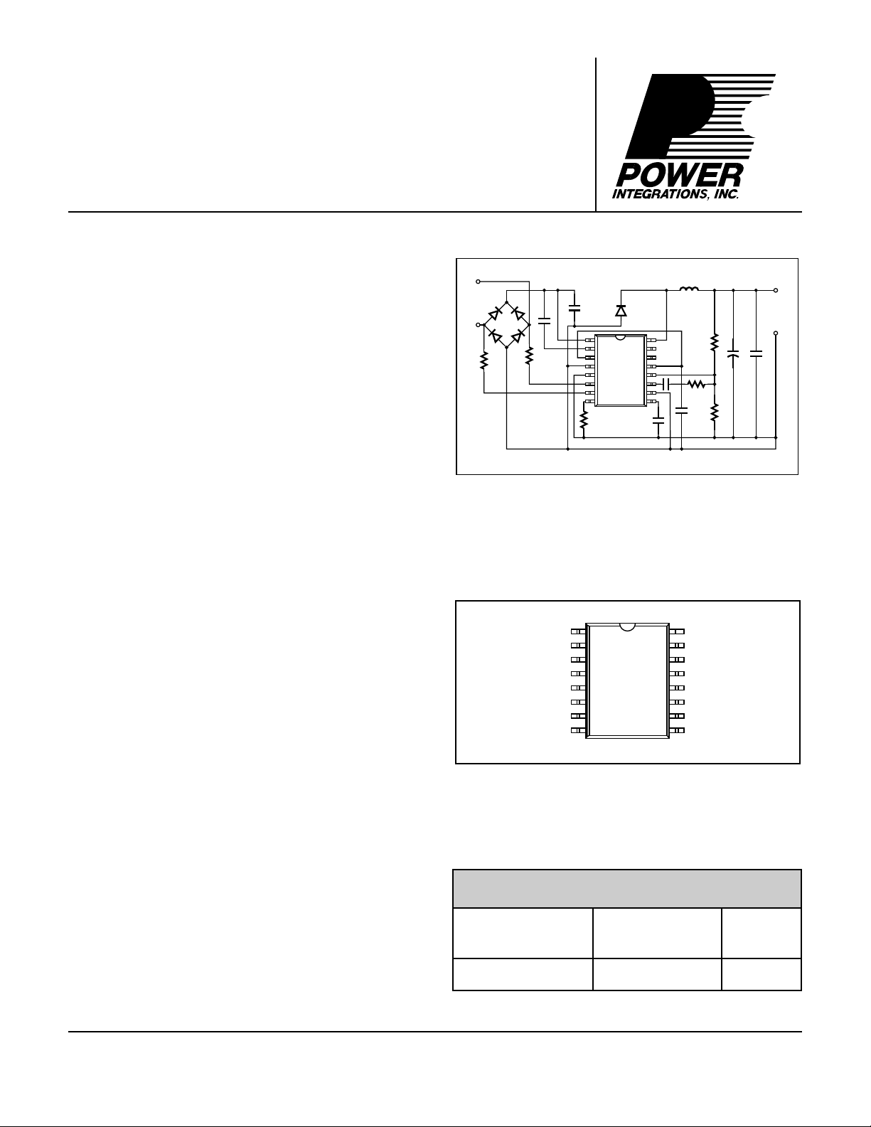
Figure 1. Typical Application.
Built-In Self-protection Circuits
• Undervoltage lockout
• Thermal shutdown
• Input polarity/level sense
®
Description
The SMP402, intended for non-isolated ISDN
telecommunications power supply applications, combines a
high voltage power MOSFET switch with a switchmode power
system controller in a monolithic integrated circuit. Few
external components are required to implement a low cost
power supply which meets stringent ISDN specifications. High
frequency operation reduces total power supply size.
The P-channel power MOSFET switch features include high
voltage, low R
results in a reduction in gate drive power, and also facilitates
higher frequency operation.
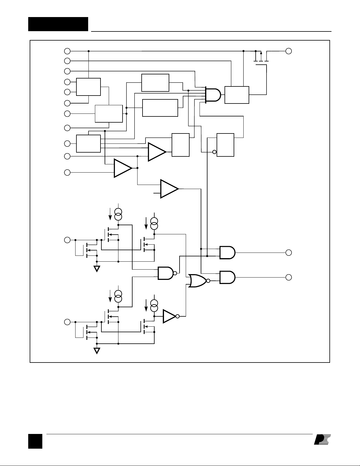
The controller section of the SMP402 contains all the blocks
required to drive and control the power stage: start-up preregulator circuit, oscillator, bandgap reference, error amplifier,
gate driver and level shift. Protection features include
undervoltage lockout, thermal shutdown, and input polarity
and level sensing.
The SMP402 is available in a 16-pin plastic SOIC package.
, and low capacitance. Lower capacitance
DS(ON)
Figure 2. Pin Configuration.
ORDERING INFORMATION
PART PACKAGE T
NUMBER OUTLINE RANGE
SMP402SC S16A 0 to 120°C
j
January 1996

SMP402
V
IN
V
LS
ENABLE
V
BIAS
V
A GND
R
EXT
D GND
C
EXT
EA OUT
EA IN
OUT
HV
S
REG
V
REF
UV
LOCKOUT
LEVEL
SHIFT
THERMAL
BANDGAP
SHUTDOWN
REF
OSC
SRQ
+
-
+
-
PWM COMPARATOR
SRQ
ERROR
AMPLIFIER
23 µA
V
S
5 µA
4 V
+
V
S
SENSE+
23 µA
SENSE-
Figure 3. Functional Block Diagram.
LEVEL
V
S
V
S
5 µA
POLARITY
PI-552B-062293
D
2
1/96

Pin Functional Description
SMP402
Pin 1:
V
is the high-voltage input to the
IN
switching regulator. This is the Source
connection of the P-Channel power
MOSFET pass transistor.
Pin 2:
V
is an internal supply for the level
LS
shift circuit that drives the P-Channel
MOSFET. A capacitor should be placed
between VLS and VIN for bypassing. V
is normally 10 V below VIN.
Pin 3:
The power supply can be shut down by
pulling ENABLE low.
Pin 4:
D GND is the common return point for
the power and logic portions of the
circuit.
Pin 5:
A GND is the common return point.
R
EXT
and C
are directly connected to
EXT
this point.
Pin 6:
The SENSE+ input monitors the polarity
and level of the input voltage through an
external resistor for ISDN emergency
Pin 11:
EA OUT is the error amplifier output
pin for connection to the external
compensation network.
standby sensing.
Pin 12:
Pin 7:
The SENSE- input monitors the polarity
and level of the input voltage through an
EA IN is the error amplifier negative
input for connection to the feedback and
compensation networks.
external resistor for ISDN emergency
LS
standby sensing.
Pin 13:
VS is the internal supply voltage. This
Pin 8:
pin is brought out for external bypassing.
A 20.5 kΩ resistor connected between
R
and A GND sets the internal bias
EXT
currents including oscillator charge and
discharge currents.
Pin 14:
The LEVEL output indicates when the
input voltage is in its normal operating
range.
Pin 9:
The oscillator frequency can be
programmed by selecting the value of
the capacitor connected between C
EXT
and A GND.
Pin 10:
V
can be connected to the output 5 V
BIAS
rail of the converter to reduce power
Pin 15:
The POLARITY output is used to notify
a microprocessor of an emergency
standby condition for ISDN applications.
Pin 16:
OUT is the Drain connection of the P-
Channel pass transistor.
dissipation. The internal 5 V regulator is
cut off when the output is in regulation.
Functional Description
High Voltage Regulator
The high-voltage regulator provides the
bias current required by the controller
and driver circuitry. The pre-regulator
consists of a high voltage MOSFET, a
gate bias current source, and an error
amplifier. The error amplifier regulates
VS to approximately 5 V by controlling
the gate of the MOSFET.
In 5 V output applications, the control
circuitry may also be operated by
connecting the V
V rail of the converter to reduce power
dissipation. The internal 5 V regulator is
cut off automatically when the converter
output is in regulation. Only the supply
pin to the output 5
BIAS
current for the level shift stage (≈50 µA)
and the AC switching currents for the PChannel output device are drawn from
the VIN supply under this condition. If
unused, V
must be hardwired to A
BIAS
GND to disable the automatic switchover
during power-up.
VLS is the level-shift supply for driving
the gate of the internal P-channel
MOSFET. The voltage at VLS is
approximately 10 V below VIN. VS is the
supply voltage for the controller and
driver circuitry. External bypass
capacitors connected to VLS and VS are
required for filtering and reducing noise.
UV Lockout
During power-up, the undervoltage
lockout circuit keeps the P-channel
output transistor in the off state until the
internal VS supply is in regulation and
the voltage sensed by the input monitor
circuit is within the normal operation
range (>12 V).
Band Gap Reference
V
is the 1.3 V reference voltage
REF
generated by the temperature-
compensated bandgap reference and
buffer. This voltage is used for setting
thresholds for the error amplifier and
over temperature circuit.
D
3
1/96

SMP402
Functional Description (cont.)
Oscillator
The oscillator frequency can be adjusted
by changing the external C
capacitor.
EXT
This capacitor is charged and discharged
by switched constant current sources.
The voltage switch points are determined
by hysteresis built into a comparator.
The period of the waveform is
determined by values of the current
sources which set the rising and falling
slopes of the sawtooth waveform.
Maximum duty cycle is equal to the ratio
of the charge time to the period. Clock
and blanking signals are synthesized
from the comparator output for use by
the modulator.
Error Amplifier
The error amplifier consists of a high
performance operational amplifier with
the non-inverting input connected to the
internal bandgap reference voltage. The
output of the error amplifier directly
controls the duty cycle of the power
switch.
Pulse Width Modulator
The pulse width modulator implements
a voltage-mode control loop, and
generates the digital driver signal which
controls the power switch. The duty
cycle of the driver signal will change as
a function of input voltage and load.
Increasing the duty cycle causes the
power supply output voltage to go up.
Conversely, decreasing the duty cycle
causes the output voltage to go down.
The pulse width modulator compares
the control voltage (error amplifier
output) with the sawtooth voltage
generated by the oscillator to produce
the required duty cycle.
Thermal Shutdown
Temperature protection is provided by a
precision analog circuit that turns the
power switch off when the junction gets
too hot (typically 140°C). The device
will automatically reset and turn back on
again when the junction has cooled past
the hysteresis temperature level.
SENSE+ and SENSE- Inputs
SENSE+ and SENSE-are both current
mirror inputs consisting of N-channel
MOSFETs connected as diodes. The
threshold voltage of each transistor is
typically 1.7 V. An input current which
exceeds the indicated threshold current
will turn on the mirror transistor for an
active-low signal.
POLARITY and LEVEL Outputs
The LEVEL output is high when the
input current to either SENSE+ or
SENSE- exceeds the LEVEL current
threshold and the output voltage is in
regulation. During normal operation,
the POLARITY output is high when the
input current to SENSE+ is above the
POLARITY current threshold and the
output voltage is in regulation. During
emergency operation (when the DC
input voltage is inverted), the
POLARITY output is low when the input
current to SENSE- exceeds the
48 V
32 V
INPUT
5 V OUT
LEVEL
POLARITY
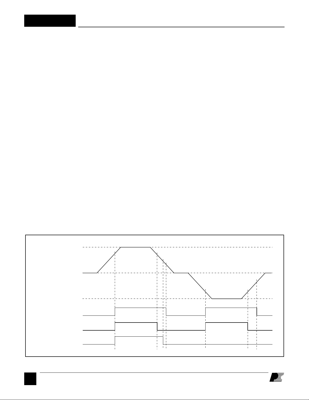
Figure 4. Turn-on and Turn-off Waveforms of the SMP402.
D
4
1/96
0
-48 V
5 V
0 V
5 V
0 V
5 V
0 V
30 V
12 V
10 V
-32 V
-10 V
-30 V
PI-960A-032293

Functional Description (cont.)
SMP402
POLARITY current threshold.
Regulation of the output voltage is
detected by a comparator which looks
for error amplifier saturation in the output
high (maximum duty cycle) state.
Power supply turn on and turn off with a
slowly changing input voltage is shown
in Figure 4 as measured using the circuit
shown in Figure 6. Also shown are the
level and polarity outputs. The input
voltage must rise above 32 V before the
SMP402 will turn on. At this input
voltage the current through R1 into the
SENSE+ input exceeds the threshold
current (typically 23 µA), the LEVEL
and POLARITY outputs go high, and
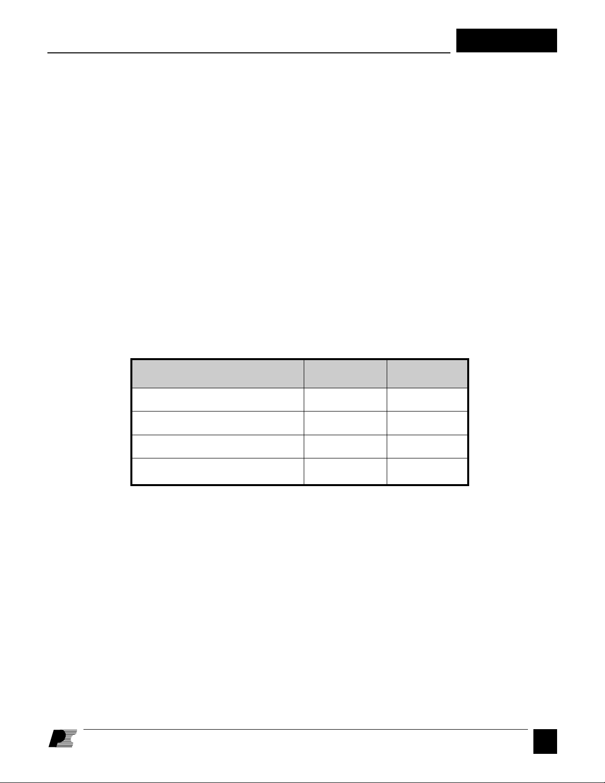
INPUT VOLTAGE CONDITION POLARITY LEVEL
the power supply turns on. As the input
voltage goes down, LEVEL will go low
at approximately 30 V, but POLARITY
will stay high. As the input voltage
continues to drop, POLARITY goes low
at approximately 12 V and the converter
loses regulation at approximately 10 V
and turns off. The LEVEL output will
go high and the power supply turns on
when the input voltage reaches -32 V.
POLARITY stays low to indicate that
the input voltage has reversed polarity.
As the negative input voltage falls toward
zero, LEVEL goes low at approximately
-30 V and the converter loses regulation
and turns off at approximately -10 V.
Enable
The power supply can be shut down by
pulling the ENABLE pin low. It is
internally pulled up to VS with a 100 µA
(nominal) current source. However, it is
recommended that this pin be tied to V
if it is unused.
P-Channel Output Transistor
The output MOSFET is a 90 V pass
transistor capable of supplying >200
mA. To minimize switching noise and
EMI, it is important to keep the path
from OUT through the output diode, the
input storage capacitor, and into VIN as
short as possible.
S
Negative voltage, level too low 0 0
Negative voltage, correct level 0 1
Positive voltage, level too low 1 0
Positive voltage, correct level 1 1
Figure 5. LEVEL/POLARITY Truth Table. The LEVEL and POLARITY signals are only valid when the output voltage is in regulation.
1/96
D
5
 Loading...