RD9
TM
TinySwitch
Flyback Prototyping Board
User Configurable Input and Output Voltages
Product Highlights
Unpopulated Prototyping Board
• Complete layout for construction of TinySwitch flyback
supply
• Convenient prototyping area on secondary side of board
• Single-sided construction
• RD9 boards can be combined for rapid prototyping with
RD8 (available separately)
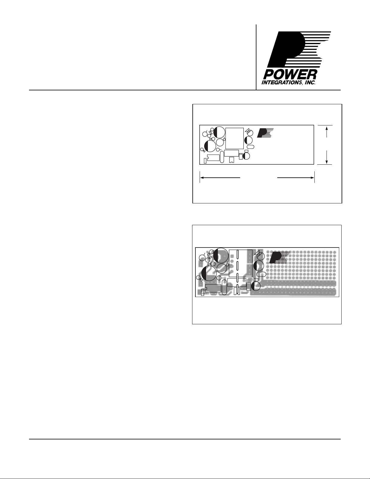
3.86 in. (97.9 mm)
Figure 1. RD9 Board Overall Physical Dimensions.
POWER
INTEGRATI ONS, INC
TinySwitch
RD9 Rev. B
®
®
.
1.31 in.
(33.2 mm)
PI-2313-0092398
Description
The RD9 is a special printed circuit board (Figure 1) designed
for rapid prototyping of TinySwitch-based flyback power
supplies in the 1-3 W range. Component positions and an
optimized layout are provided for a complete single output
power supply as shown in Figure 2. Component size and
placement are identical to evaluation board RD8. The board is
designed to accommodate a transformer using an EE16 core
with a 10 pin bobbin (Ying Chin YC-1607 or equivalent*). In
addition to the power supply circuitry, the RD9 also provides a
prototyping area on the secondary side of the board for circuitry
such as additional outputs or voltage and current regulators.
Some typical application circuits that can be constructed using
the RD9 printed circuit board can be found in the TinySwitch
and RD8 data sheets, and Design Ideas DI-4 through DI-8.
For extremely rapid prototyping, the RD8 TinySwitch evaluation
board and the RD9 prototyping board are perforated between
the primary and secondary circuit areas, so that the primary half
of the RD8 can be separated and combined with the secondary
half of the RD9.
D1
R1
L
D3
C2
D4
N
U1
C4
C1
D2
L1
R2
R4
C3
U2
T1
C6
EE16_10P2
L2
JMP1
C5
+
C7
VR1
[Not Actual Size]
TinySwitch
Figure 2. PC Board Layout of the RD9.
POWER
INTEGRA TIONS, INC
RD9 Rev. B
PI-2319-100898
®
.
* Available from B&B Products Corp +1 (520) 884-4818
September 1998

RD9
L1
AC
D1
R1
Fusible
D2
C1
R2
R4
C2
Input
C3
D3
D4
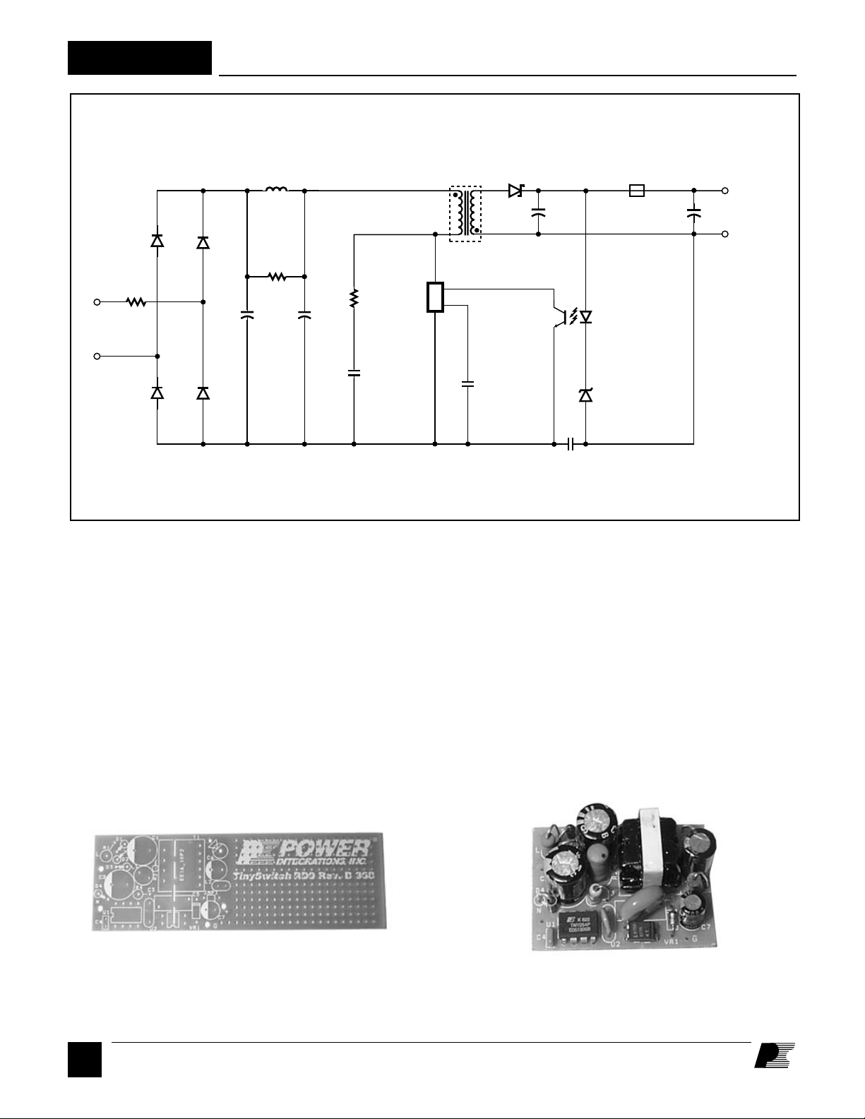
Figure 3. Schematic Diagram of a Typical RD9 Circuit.
3
4
TinySwitch
D
EN
BP
U1
S
T1
8-10
5-7
C4
D5
U2
C6
L2
Bead
Output
C7
RTN
VR1
C5
PI-2315-092298
Using RD8 and RD9 Together
A complete RD9 board is shown in Figure 4, and an RD8 board
in Figure 5. To combine the secondary side of RD9 with the
primary side of RD8, follow the instructions below:
Figure 4. RD9 Printed Circuit Board.
A
2
9/98
Figure 5. RD8 Printed Circuit Board.

• Break the RD9 board along the perforations to separate the
primary and secondary halves. The secondary half of the
board contains the prototyping area (Figure 6).
RD9
Figure 6. Prepared RD9 Board.
• Prepare the RD8 board by removing T1, C5, and U2. Set
these aside for reuse. Break the board along the perforations
to separate the primary and secondary circuitry. The board
should then look as shown in Figure 7.
• Fit the primary half of RD8 and the secondary half of RD9
together, using T1, C5, and U2 removed from the RD8
board to bridge between the two board halves (Figure 8). A
different transformer can be substituted for T1. Use the
cores and bobbins suggested in the text for best mechanical
fit.
Figure 7. Prepared RD8 Board.
Figure 8. Combined RD8 and RD9.
9/98
A
3

RD9
For the latest updates, visit our website: www.powerint.com
Power Integrations reserves the right to make changes to its products at any time to improve reliability or manufacturability.
Power Integrations does not assume any liability arising from the use of any device or circuit described herein, nor does it
convey any license under its patent rights or the rights of others.
PI Logo and
TOPSwitch
are registered trademarks of Power Integrations, Inc.
©Copyright 1998, Power Integrations, Inc. 477 N. Mathilda Avenue, Sunnyvale, CA 94086
WORLD HEADQUARTERS
NORTH AMERICA - WEST
Power Integrations, Inc.
477 N. Mathilda Avenue
Sunnyvale, CA 94086 USA
Main: +1•408•523•9200
Customer Service:
Phone: +1•408•523•9265
Fax: +1•408•523•9365
KOREA
Power Integrations International
Holdings, Inc.
Rm# 402, Handuk Building,
649-4 Yeoksam-Dong, Kangnam-Gu,
Seoul, Korea
Phone: +82•2•568•7520
Fax: +82•2•568•7474
A
4
9/98
NORTH AMERICA - EAST
& SOUTH AMERICA
Power Integrations, Inc.
Eastern Area Sales Office
1343 Canton Road, Suite C1
Marietta, GA 30066 USA
Phone: +1•770•424•5152
Fax: +1•770•424•6567
JAPAN
Power Integrations, K.K.
Keihin-Tatemono 1st Bldg.
12-20 Shin-Yokohama 2-Chome,
Kohoku-ku, Yokohama-shi,
Kanagawa 222, Japan
Phone: +81•45•471•1021
Fax: +81•45•471•3717
EUROPE & AFRICA
Power Integrations (Europe) Ltd.
Mountbatten House
Fair Acres Windsor
Berkshire SL4 4LE,
United Kingdom
Phone: +44•1753•622•208
Fax: +44•1753•622•209
INDIA (Technical Support)
Innovatech
#1, 8th Main Road
Vasanthnagar
Bangalore 560052, India
Phone: +91•80•226•6023
Fax: +91•80•228•2191
TAIWAN
Power Integrations International
Holdings, Inc.
2F, #508, Chung Hsiao E. Rd., Sec. 5,
Taipei 105, Taiwan
Phone: +886•2•2727•1221
Fax: +886•2•2727•1223
APPLICATIONS HOTLINE
World Wide +1•408•523•9260
APPLICATIONS FAX
World Wide +1•408•523•9361
 Loading...