

Page 1
RD8
PI-2252-091098
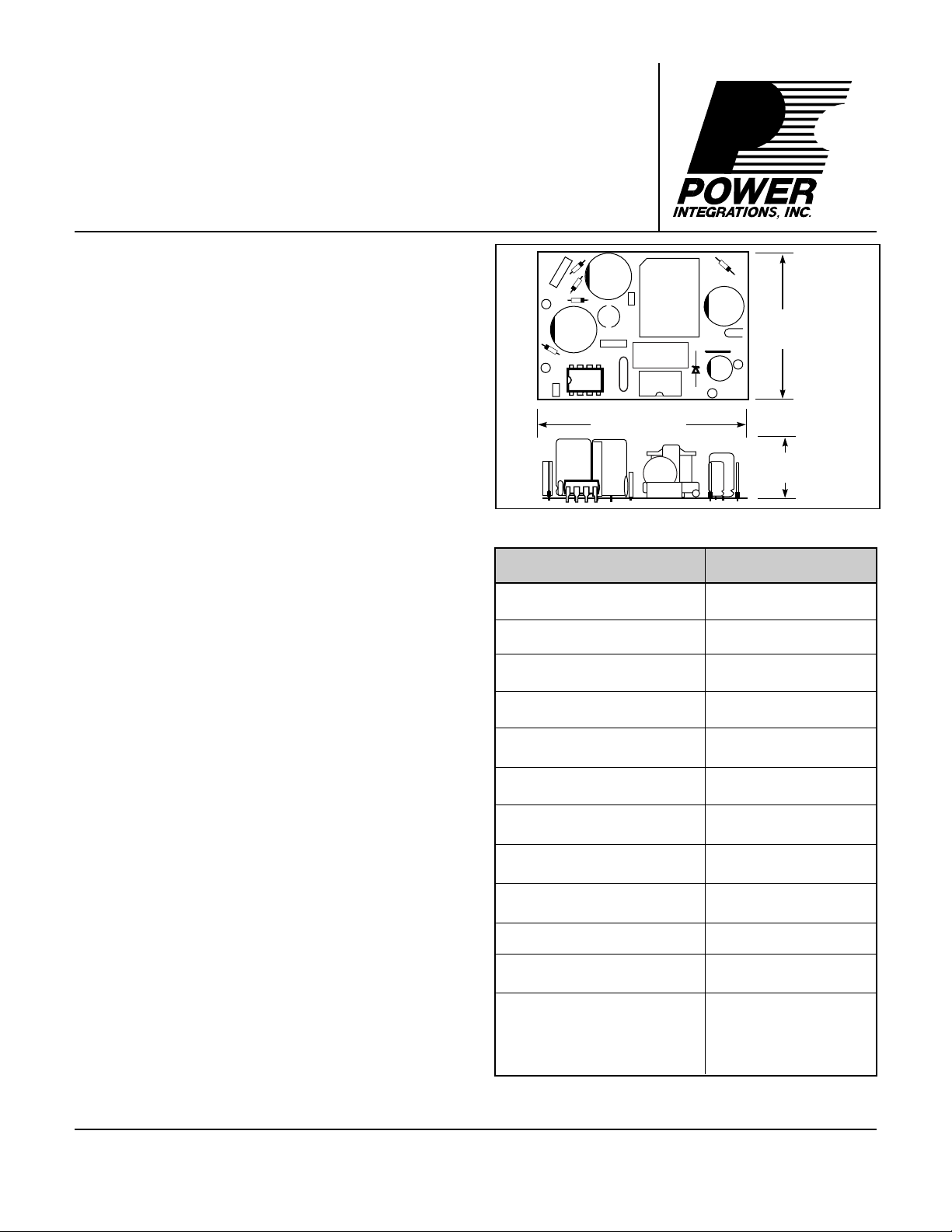
0.80 in.
(20 mm)
1.30 in.
(33 mm)
1.80 in. (45 mm)
®
TinySwitch
TM
Reference Design Board
85 to 265 VAC Input, 3 W Output
Low Cost Production Worthy AC
Adapter Reference Design
• Cost competitive with linear solutions (regulated 50/
60 Hz transformers)
• Lowest component count switching solution
• Ultra low no-load power consumption (30/70 mW @115/
230 VAC)
• Simple low cost two-winding transformer
• Greater than 72% efficiency
• Low average EMI, only one inductive component
required for EMI filtering
• Small size
Designed for World Wide Operation
• Designed for IEC/UL safety requirements
• Meets FCC/VDE Class B EMI specifications
• Wide range input voltage
Figure 1. RD8 Board Overall Physical Dimensions.
PARAMETER LIMITS
Description
The RD8 reference design board is an example of a low cost
production worthy design for an AC wall adapter or similar
applications requiring small size, high efficiency, and low cost.
The RD8 utilizes the TNY254 member of the TinySwitch
family of low cost Off-line Switchers from Power Integrations.
It is intended to help TinySwitch users develop their products
quickly by providing a production ready design which needs
little or no modification to meet system requirements. The RD8
is designed to replace conventional linear AC wall adapters,
offering universal input range, smaller size, and high efficiency,
all at a competitive cost. The RD8 is cost-competitive with
linear solutions (regulated 50/60 Hz transformers).
The unique ON/OFF control scheme of Tinyswitch virtually
eliminates energy consumption at no load. Typical linear wall
adapters consume 1-4 watts at no load, which costs $1-$4 per
year ( based on $0.12/kWhr). In comparison, a typical TinySwitch
supply consumes 30-70 mW at no load, offering substantial
energy savings.
Input Voltage Range 85 to 265 VAC
Input Frequency Range 47 to 440 Hz
Temperature Range 0 to 50°C
Output Voltage (I = 0.33 A) 9 V ± 7%*
Output Power (continuous) 3 W
Line Regulation (85-265 VAC) ± 0.5%
Load Regulation (0%-100%) ± 1%
Efficiency (PO = 3 W) 72% (min)
Standby Power Consumption
(115/230 VAC)
Output Ripple Voltage ± 75 mV
Safety IEC 950 / UL1950
EMI
* Can be improved to ± 5% by using a more accurate Zener (± 2%).
Table 1. Table of Key Electrical Parameters.
o
30/70 mW (typical)
VFG243B (Quasi-Peak)
VFG46 B (Average)
CISPR22 B
FCC Part 15 "B"
March 1999
Page 2
RD8
L1
5 mH
R2
85-265
VAC
D3
1N4005
R1
2.2 Ω
Fusible
D4
1N4005
D1
1N4005
4.7 µF
400 V
D2
1N4005
C1
4.7 kΩ
C2
4.7 µF
400 V
R4
1.5 kΩ
1/2 W
C3
68 pF
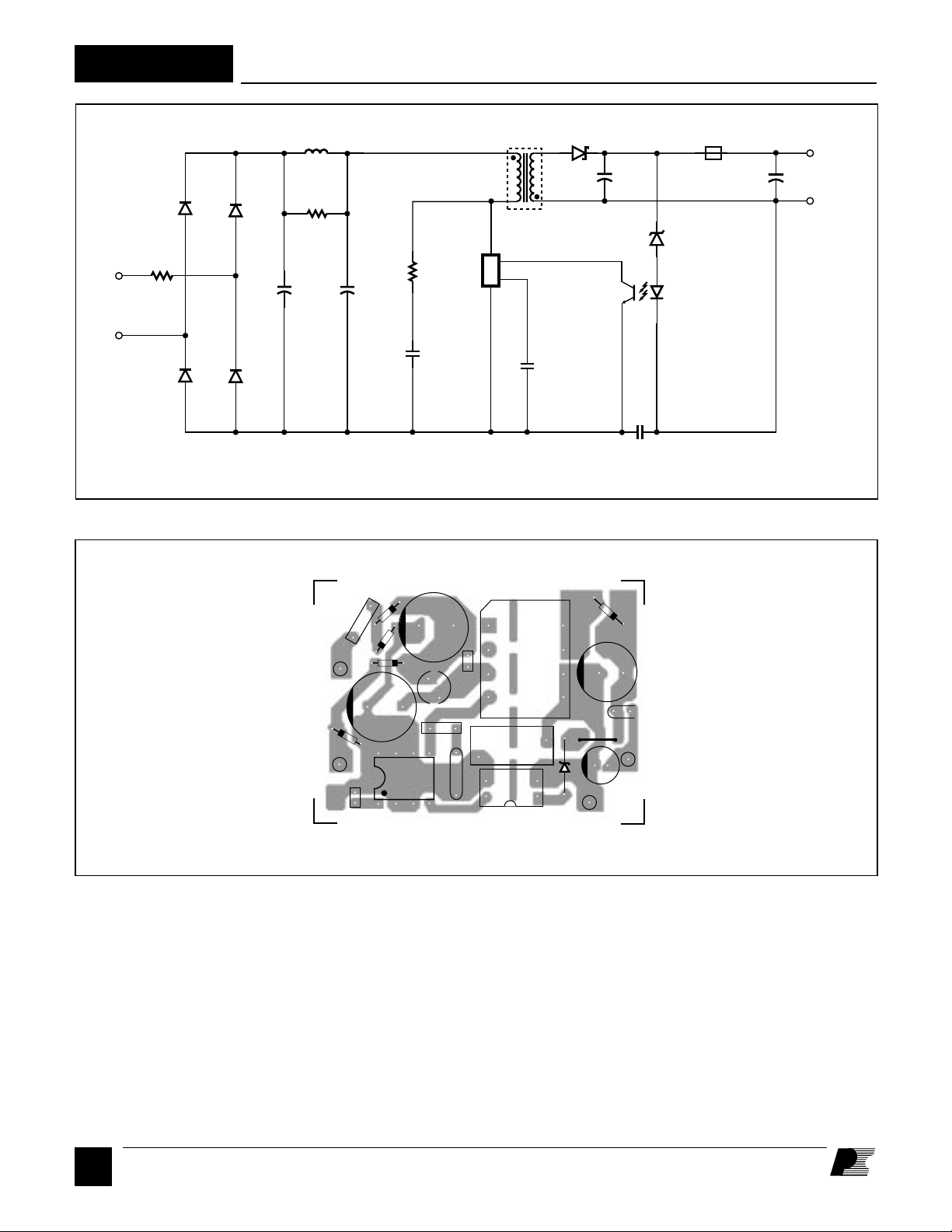
Figure 2. Schematic Diagram of the 3 W RD8 Power Supply.
U1
TNY254P
T1
3
4
TinySwitch
D
EN
BP
S
11DQ06
9
6
C4
0.1 µF
D5
U2
LTV817
C6
330 µF
16 V
C5
2.2 nF
Y1 Safety
Bead
VR1
1N5237B
L2
C7
100 µF
25 V
+ 9 V
RTN
PI-2250-090398
R1
D1
D3
D2
L1
R4
U1
L
C2
D4
N
C4
COMPONENT SIDE SHOWN*
Figure 3. Component Legend for the RD8.
General Circuit Description
The RD8 is a low-cost flyback switching power supply using
the TNY254P integrated circuit. The circuit shown in Figure 2
details a 9 V, 3 W power supply that operates from 85 to
265 VAC input voltage, suitable for replacing conventional
linear supplies in cost-sensitive applications such as AC wall
adapters.
AC power is rectified and filtered by D1-4, C1, and C2 to create
C1
R2
C3
U2
T1
C5
VR1
D5
C6
L2
Jmp 1
+
C7
G
* Shown 1.5 X actual size
the high voltage DC bus applied to the primary winding of T1.
R4 and C3 clamp the primary leakage spike and also reduce
EMI. At this power level, a simple RC network is sufficient for
snubbing leakage spikes. Because of the relatively low switching
frequency of TinySwitch (44 kHz), and its ON/OFF control
method, the additional capacitive loading of the RC snubber
network has a much smaller effect on efficiency than for
conventional PWM switchers running at higher switching
frequencies. Since TinySwitch runs in current limit mode at all
times regardless of output load, the worst case leakage spike
PI-2254-091597
C
2
3/99
Page 3

Component Listing
Reference Value Part Number Manufacturer
C1, C2 4.7 µF, 400 V 475CKH400M Illinois Capacitors
C3 68 pF, 1 kV DD680 Philips
C4 0.1 µF, 50 V RPE121Z5U104M50V Murata
C5 2.2 nF, 250 VAC Y1 440LD22 Cera-Mite
C6 330 µF, 16 V Low ESR ECA-1CFQ331L Panasonic
C7 100 µF, 25 V ECE-A1EGE101 Panasonic
D1-4 600 V, 1 A 1N4005 General Instrument
D5 60 V, 1A, Schottky 11DQ06 International Rectifier
L1 5.5 mH (min), 0.1 A
L2 Ferrite Bead, 3.5 X 11.4 mm 2743008112 Fair-Rite
R1 2.2 Ω, 1 W BW2F2.2Ω5% RCD
R2 4.7 kΩ, 1/4 W 5043CX4K700J Philips
R4 1.5 kΩ, 1/2 W, 5% 5053CX1K500J Philips
T1* TRD8 Custom
U1 TNY254P Power Integrations
U2 Optocoupler LTV817 Liteon
VR1 8.2 V 5% Zener 1N5237B Motorola
* For transformer sources, please visit the Power Integrations website at www.powerint.com.
RD8
Table 2. Parts List for the RD8.
and the appropriate values of R4 and C3 required for snubbing
are easily determined. Traditional RCD or diode-Zener clamping
can also be used at a small additional cost for higher efficiency.
The secondary winding of T1 is rectified and filtered by D5, C6,
L2, and C7 to create the 9 V output voltage.
Zener diode VR1 and U2 sense the output voltage and provide
feedback to TinySwitch U1. The output voltage is set by the
combined voltage drops of Zener diode VR2 and the LED of
U2. Other output voltages are also possible by adjusting the
transformer turns ratio and the value of Zener diode VR1. A
resistor can be placed across the LED of U2 to provide
additional bias current (1-5 mA) to VR1. This improves
regulation and voltage accuracy. The extra bias current slightly
increases no load power consumption (15-75 mW).
Capacitors C1, C2, L1, R2, and Y1-capacitor C5 provide EMI
filtering for the power supply. At lower output power levels (or
for supplies designed to operate at 115 VAC only), L1 can be
replaced with a resistor, reducing system cost at the expense of
slightly lower efficiency.
on-time for each switching cycle is set by the transformer
primary inductance, TinySwitch current limit and the high
voltage DC input bus. Output regulation is accomplished by
skipping switching cycles in response to an ON/OFF feedback
signal applied to the ENABLE pin. This differs significantly
from traditional PWM schemes that control the duty factor of
each switching cycle. Due to the ON/OFF nature of the
TinySwitch control scheme, the feedback optocoupler operates
in switching rather than in linear mode. Therefore the current
transfer ratio is not a critical factor as long as the optocoupler
provides enough current (50 µA) to activate the ENABLE pin
of the TinySwitch. This allows a low cost ungraded optocoupler
to be used.
For 115 V applications, 200 V rated capacitors can be used for
C1 and C2, and D5 can be replaced with a 40 V device (1N5819
or similar). If 200 V capacitors are used, then L1 can be
replaced with a resistor.
The circuit performance data shown in Figures 4-17 were
measured with AC voltage applied to the RD8.
Resistor R1 is a fusible resistor for protection against primary
fault conditions. This is a low cost alternative to a standard fuse,
accepted by safety agencies.
The RD8 power supply is designed to run in discontinuous
conduction mode, with the primary peak current set by the
TNY254P internal current limit. In this mode of operation, the
Load Regulation (Figure 4) – The change in the DC output
voltage for a given change in output current is referred to as load
regulation. RD8 output voltage stays within ± 1% of nominal
from 0% to 100% of rated load current. The TinySwitch
regulation scheme enables this level of performance without the
use of a preload. The slight rise in output voltage at no load is
due to an increase in the voltage drop across VR1, caused by
C
3
3/99
Page 4

RD8
General Circuit Description (cont.)
higher average Zener current. This effect can be corrected by
adding a Zener bias resistor across the LED side of U2. This
resistor also provides a small preload, further improving no load
regulation.
Line Regulation (Figure 5) - The change in the DC output
voltage for a given change in the AC input voltage is called line
regulation. The maximum change in output voltage versus line
for the RD8 is within ± 0.5%.
Efficiency (Line Dependent) – Efficiency is the ratio of the
output power to the input power. The curves in Figures 6 and 7
show the efficiency as a function of input voltage. Note that the
efficiency is relatively constant over the entire input voltage
range.
Efficiency (Load Dependent) – The curves in Figures 8 and 9
show how the efficiency changes with output power for 115 VAC
and 230 VAC inputs. Due to the TinySwitch regulation scheme,
the efficiency is relatively constant from 0-100% of output load.
Power Supply Turn On Sequence –The waveforms shown in
Figure 10 illustrate the relationship between the high-voltage
DC bus and the 9 V output voltage. Since the TinySwitch
internal power consumption is extremely small and is derived
entirely from the DRAIN, the supply starts switching almost as
soon as power is applied, as shown in Figure 10. The output
achieves regulation approximately 8 ms after power is applied,
with no overshoot.
Power Supply Turn Off Sequence - Figure 11 shows the decay
of the 9 V output when the AC input is removed. The 9 V
decays monotonically to zero after AC power is removed, with
no spurious pulses.
Output Ripple - Line frequency ripple voltage is shown in
Figure 12 for 115 VAC input and 3 W output. Switching
frequency ripple voltage is shown in Figure 13 for the same test
condition. In Figure 13, note the skipped pulses due to the
TinySwitch ON/OFF control.
The RD8 is designed to meet worldwide safety and EMI (FCC
B and VDE B) specifications. Measured conducted emissions
are shown in Figure 16 for 115 VAC and Figure 17 for
230 VAC. In the RFI measurements performed on the RD8,
peak measurements were applied to the quasi-peak limits
specified by the test agencies. A peak measurement is more
stringent than a quasi-peak or average measurement, since there
is no averaging of the EMI signal form the supply under test.
Peak measurements are also simpler and easier to perform using
a standard spectrum analyzer.
Figure 16 shows the results of a peak EMI scan at 115 VAC and
full output load, compared to the FCC B quasi-peak limit. The
RD8 passes the FCC B quasi-peak limits with margin using a
peak EMI measurement. Applying quasi-peak measurement to
the RD8 will result in EMI levels 3-4 dB lower than shown in
Figure 16. This is true because the RD8 skips pulses to achieve
regulation, resulting in substantially lower quasi-peak and
average EMI levels than for a peak measurement.
Most European EMI standards specify test limits for both
quasi-peak and average measurement. The supply under test
must pass both the average and quasi-peak limits to achieve
certification. Figure 17 shows peak and average EMI scans
performed at 230 VAC input and full load, compared to the
VFG243 B quasi-peak limit and the VFG46 B average limit.
The VFG243 and VFG46 specifications incorporate the same
test limits as CISPR22, but also include frequencies below
150 kHz. The RD8 peak measurement passes the VFG 243 B
quasi-peak limit with substantial margin, and almost passes the
VFG46 B average limit. The average measurement passes the
VFG46 B average limit with a minimum of 6 dB margin.
In both the 115 V and 230 V measurements, there is almost no
EMI at frequencies of 4 MHz and above. This is due in part to
the relatively low operating frequency of TinySwitch (44 kHz
nominal). The lack of high frequency emissions allows easy
compliance with international radiated emissions limits.
Transformer Specification
Load Transient Response - The output transient response to a
step load change from 0.26 to 0.33 A (75% to 100%) is shown
in Figure 14. Note that the load transient is extremely small
(< 20 mV), and recovers within 100 µs. The small step in the
load response is due to the finite load regulation of the RD8.
No Load Power Consumption - Figure 15 shows no load power
consumption as a function of input voltage. The no load power
consumption for the RD8 is only 10 to 20% of the standby
power consumption of a typical linear power supply.
C
4
3/99
The electrical specifications and construction details for
transformer TRD8 are shown in Figures 18 and 19. Transformer
TRD8 is supplied with the RD8 reference design board. Since
no auxiliary bias winding is required to power TinySwitch, the
transformer design is very simple, requiring only a primary and
secondary winding.
The TRD8 design utilizes an EE16 core and a triple insulated
wire secondary winding. The use of triple insulated wire allows
the transformer to be constructed using a smaller core and
bobbin than a conventional magnet wire design due to the
Page 5

RD8
elimination of the margins required for safety spacing in a
conventional design.
If a conventional margin wound transformer is desired, the
design of Figures 20-21 can be used. This design (TRD8-1)
uses an EEL16 core and bobbin to accommodate the 6 mm total
creepage distance required to meet international safety standards
105
100
95
0
100
Load Current (mA)
105
100
Output Voltage (% of Nominal)
95
0 100 200 300
Load Current (mA)
VIN = 115 VAC
200 300
VIN = 230 VAC
PI-2256-091698
400
400
when using magnet wire rather than triple insulated wire. It has
the same pinout and printed circuit foot print as TRD8. The
margin wound transformer is approximately 50% taller than the
triple insulated wire design due to the inclusion of creepage
margins required to meet international safety standards.
105
100
95
50 100 150 200 250 300
Input Voltage (VAC)
105
100
Output Voltage (% of Nominal)
95
50 100 150 200 250 300
PO = 0.6 W
Input Voltage (VAC)
PO = 3 W
PI-2258-091698
Figure 4. Load Regulation. Figure 5. Line Regulation.
100
Po = 3 W
80
60
40
20
Output Efficiency (%)
0
50 100 300200
Input Voltage (VAC)
PI-2260-091698
100
Po = 0.6 W
80
60
40
Output Efficiency (%)
20
0
50 100 300200
Input Voltage (VAC)
Figure 6. Efficiency vs. Input Voltage, 3 W Output. Figure 7. Efficiency vs. Input Voltage, 0.6 W Output.
PI-2262-091698
3/99
C
5
Page 6

RD8
100
VIN = 115 VAC
80
60
40
Output Efficiency (%)
20
0
0.5
01 32
1.5
2.5
Output Power (W)
Figure 8. Efficiency vs. Output Power, 115 VAC Input.
DC BUS VOLTAGE
150
100
50
PI-2264-091798
PI-2268-101598
100
VIN = 230 VAC
80
60
40
Output Efficiency (%)
20
0
0.5
01 32
1.5
2.5
Output Power (W)
Figure 9. Efficiency vs. Output Power, 230 VAC Input.
14
12
10
PI-2266-091798
PI-2270-101598
10
0
OUTPUT
VOLTAGE
5
0
0
10 20
8
6
Output Voltage (V)
4
2
0
0
Time (ms)
Figure 10. Turn On Delay, 115 VAC Input. Figure 11. Output Turn Off.
60
40
20
0
-20
Output Voltage (mV)
-40
-60
PI-2272-101598
100
50
0
-50
Output Voltage (mV)
-100
12
Time (s)
PI-2274-101598
0
25 50
Time (ms)
Figure 12. Line Frequency Ripple, 115 VAC Input, 3 W Output.
C
6
3/99
0
100 200
Time (µs)
Figure 13. Switching Frequency Ripple, 115 VAC Input, 3 W
Output.
Page 7

RD8
20
0
-20
PI-2276-101598
Output Voltage (mV)
300
200
100
0
Output Current (A)
012
Time (ms)
Figure 14. Transient Load Response (75% to 100% of load).
120
100
80
60
PI-2284-101698
Figure 15. No Load Power Consumption.
80
60
40
Power (mW)
20
0
50 100 150 200 250 300
PO = 0 W
AC Input Voltage (V)
120
VFG243B (QP)
100
80
60
VFG46B (AV)
Peak Scan
Average Scan
PI-2282-101698
PI-2323-101698
40
Amplitude (dBµV)
20
0
0.01 0.1
FCC 15 B (QP)
Peak Scan
1
10
Frequency (MHz)
Figure 16. EMI Characteristics at 115 VAC Input.
40
Amplitude (dBµV)
20
0
0.01 0.1
1
10
Frequency (MHz)
Figure 17. EMI Characteristics at 230 VAC Input.
3/99
C
7
Page 8

RD8
TRIPLE INSULATED SECONDARY TRANSFORMER (TRD8)
3
174 T
#34 AWG
4
CORE# - PC40 EE16-Z (TDK)
GAP FOR AL OF 112 nH/T
9
14 T
#26 AWG
Triple-insulated
6
2
BOBBIN# - YC-1607 (Ying Chin Co., Ltd.)
ELECTRICAL SPECIFICATIONS
Electrical Strength
Creepage
Primary Inductance
Resonant Frequency
PIN FUNCTION
3
HIGH-VOLTAGE DC BUS
4
TinySwitch
6
SECONDARY RETURN
9
OUTPUT
60 Hz, 1 minute,
from pins 1-4 to pins 5-10
Between pins 1-4 and pins 5-10
All windings open
All windings open
DRAIN
1
4
3000 VAC
6.00 mm (min)
3400 µH ±10%
420 kHz (min)
10
5
Primary Leakage Inductance
NOTE: All inductance measurements should be made at 40 kHz
Figure 18. Electrical specification of transformer TRD8.
Pins 6 and 9 shorted
120 µH (max)
PI-2226-082498
C
8
3/99
Page 9

TRIPLE INSULATED SECONDARY TRANSFORMER CONSTRUCTION
RD8
WINDING INSTRUCTIONS
Primary
Secondary Winding
Final Assembly
* Triple insulated wire sources.
P/N: T27A01TXXX-3
Rubudue Wire Company
5150 E. La Palma Avenue
Suite 108
Anaheim Hills, CA 92807
(714) 693-5512
(714) 693-5515 FAX
9
6
4
3
Start at Pin 3. Wind 174 turns of 34 AWG heavy nyleze
wire in four layers. Finish on Pin 4.
Start at Pin 6. Wind 14 turns of 26 AWG
from left to right. Finish on Pin 9.
Assemble and secure core halves. Glue according to
Power Integrations instructions (see Power Integrations
website:
www.powerint.com
P/N: order by description
Furukawa Electric America, Inc.
200 Westpark Drive
Suite 190
Peachtree City, GA 30269
(770) 487-1234
(770) 487-9910 FAX
SECONDARY
PRIMARY
triple insulated wire
).
P/N: order by description
The Furukawa Electric Co., Ltd
6-1, Marunouchi 2-chome,
Chiyoda-ku, Tokyo 100, Japan
81-3-3286-3226
81-3-3286-3747 FAX
Figure 19. Construction details of transformer TRD8.
PI-2228-082498
C
9
3/99
Page 10

RD8
MARGIN WOUND TRANSFORMER
3
174 T
#34 AWG
4
CORE# - PC40 EE16/24/5-Z (TDK)
GAP FOR AL OF 182 nH/T
BOBBIN# - YC1605 (Ying Chin Co., Ltd.)
9
14 T
#26 AWG
6
2
ELECTRICAL SPECIFICATIONS
Electrical Strength
Creepage
Primary Inductance
PIN FUNCTION
3
HIGH-VOLTAGE DC BUS
4
TinySwitch
6
RETURN
9
OUTPUT
60 Hz, 1 minute,
from pins 1-4 to pins 5-10
Between pins 1-4 and pins 5-10
All windings open
DRAIN
10
1
3000 VAC
6.0 mm (min)
3400 µH ±10%
5
4
Resonant Frequency
Primary Leakage Inductance
NOTE: All inductance measurements should be made at 40 kHz
Figure 20. Electrical specification of transformer TRD8-1.
All windings open
Pins 6 and 9 shorted
420 kHz (min)
120 µH (max)
PI-2222-082198
10
C
3/99
Page 11

MARGIN WOUND TRANSFORMER CONSTRUCTION
TAPE MARGINS
(2 PLACES)
SECONDARY
TAPE
9
6
RD8
4
TAPE
3
WINDING INSTRUCTIONS
Primary
Reinforced Insulation
Safety Margin
Secondary Winding
Outer Insulation
PRIMARY
Start at Pin 3. Wind 174 turns of 34 AWG heavy nyleze
wire in four layers. Finish on Pin 4.
Apply 3 layers of tape (polyester film, 17.5 mm (0.689 in)
wide and 0.056 mm (2.2 mil) thick) for reinforced
insulation.
Construct margins on each side of bobbin using 3 mm
wide tape on flange side of bobbin and 6 mm wide tape
on pin side of bobbin. Match height of secondary winding.
Start at Pin 6. Wind 14 turns of 26 AWG heavy nyleze wire
from left to right in a single layer. Finish on Pin 9.
Apply 3 layers of 17.5 mm tape for outer insulation.
Final Assembly
Figure 21. Construction details of transformer TRD8-1.
Assemble and secure core halves. Glue according to
Power Integrations instructions (see Power Integrations
website:
www.powerint.com
).
PI-2224-082498
C
11
3/99
Page 12

RD8
For the latest updates, visit our website: www.powerint.com
Power Integrations reserves the right to make changes to its products at any time to improve reliability or manufacturability.
Power Integrations does not assume any liability arising from the use of any device or circuit described herein, nor does it
convey any license under its patent rights or the rights of others.
PI Logo and
TOPSwitch
are registered trademarks of Power Integrations, Inc.
©Copyright 1999, Power Integrations, Inc. 477 N. Mathilda Avenue, Sunnyvale, CA 94086
WORLD HEADQUARTERS
NORTH AMERICA - WEST
Power Integrations, Inc.
477 N. Mathilda Avenue
Sunnyvale, CA 94086 USA
Main: +1•408•523•9200
Customer Service:
Phone: +1•408•523•9265
Fax: +1•408•523•9365
KOREA
Power Integrations International
Holdings, Inc.
Rm# 402, Handuk Building,
649-4 Yeoksam-Dong, Kangnam-Gu,
Seoul, Korea
Phone: +82•2•568•7520
Fax: +82•2•568•7474
NORTH AMERICA - EAST
& SOUTH AMERICA
Power Integrations, Inc.
Eastern Area Sales Office
1343 Canton Road, Suite C1
Marietta, GA 30066 USA
Phone: +1•770•424•5152
Fax: +1•770•424•6567
JAPAN
Power Integrations, K.K.
Keihin-Tatemono 1st Bldg.
12-20 Shin-Yokohama 2-Chome,
Kohoku-ku, Yokohama-shi,
Kanagawa 222, Japan
Phone: +81•45•471•1021
Fax: +81•45•471•3717
EUROPE & AFRICA
Power Integrations (Europe) Ltd.
Centennial Court
Easthampstead Road
Bracknell
Berkshire RG12 1YQ,
United Kingdom
Phone: +44•1753•622•208
Fax: +44•1753•622•209
INDIA (Technical Support)
Innovatech
#1, 8th Main Road
Vasanthnagar
Bangalore 560052, India
Phone: +91•80•226•6023
Fax: +91•80•228•2191
TAIWAN
Power Integrations International
Holdings, Inc.
2F, #508, Chung Hsiao E. Rd., Sec. 5,
Taipei 105, Taiwan
Phone: +886•2•2727•1221
Fax: +886•2•2727•1223
APPLICATIONS HOTLINE
World Wide +1•408•523•9260
APPLICATIONS FAX
World Wide +1•408•523•9361
12
C
3/99
 Loading...