

February 1996
Product Highlights
Floating Control Inputs
• Connects directly to INT200 or INT202 HSD outputs
• No external level translators or transformers required
Gate Drive Output for an External MOSFET
• Provides 300 mA sink/150 mA source current
• Can drive MOSFET gate at up to 15 V
• Floating source for driving high-side N-channel MOSFET
• External MOSFET allows flexibility in design for various
motor sizes
Built-in Protection Circuits
• Logic inputs include noise rejection circuitry
• Undervoltage lockout
Description
The INT201 high-side driver IC provides gate drive for an
external high-side MOSFET switch. When used in conjunction
with the INT200 or INT202 low-side drivers, the INT201
provides a simple, cost-effective interface between low-voltage
control logic and high-voltage loads.
Built-in noise rejection circuitry shared between the INT201
and the INT200 or INT202 provides reliable operation in the
harshest industrial environments. The INT201 is powered from
a ground-referenced low-voltage supply. A floating supply is
derived from this rail by using a simple bootstrap technique to
provide adequate gate drive for the external N-channel MOSFET.
Applications include motor drives, electronic ballasts, and
uninterruptible power supplies. The INT201 can also be used
to implement full-bridge and multi-phase configurations.
The INT201 is available in 8-pin plastic DIP and SOIC packages.
INT201
High-side Driver IC
Floating Inputs
Floating High-side Drive
®
ORDERING INFORMATION
PART PACKAGE TEMP
NUMBER OUTLINE RANGE
INT201PFI P08A -40 to 85°C
INT201TFI T08A -40 to 85°C
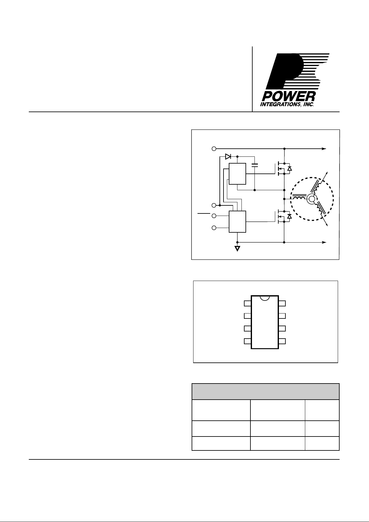
Figure 1. Typical Application.
Figure 2. Pin Configuration.
PI–285D–091191
HSD2
8
5
7
6
SOURCE
HS OUT
N/C
HSD1
1
4
2
3
V
DDH
N/C
N/C
HV
HS IN
LS IN
INT201
INT200
PI-1764-020196
V
DD
3-PHASE
BRUSHLESS
DC MOTOR
INT201
F
2/96
2
Pin Functional Description
Pin 1:
No connection.
Pin 2:
No connection.
Pin 3:
Level shift input HSD 1 works in
conjunction with HSD 2 to provide
interface from the low side control logic
and to give noise immunity.
Pin 4:
Level shift input HSD 2 works in
conjunction with HSD 1 to provide
interface from the low side control logic
and to give noise immunity.
Pin 5:
SOURCE connection. Analog reference
point for the circuit, normally connected
to the source of the high side MOSFET.
Pin 6:
HS OUT is the output of the MOSFET
driver for the high side.
Pin 7:
No connection.
Pin 8:
V
DDH
supplies power to the control logic
and output driver.
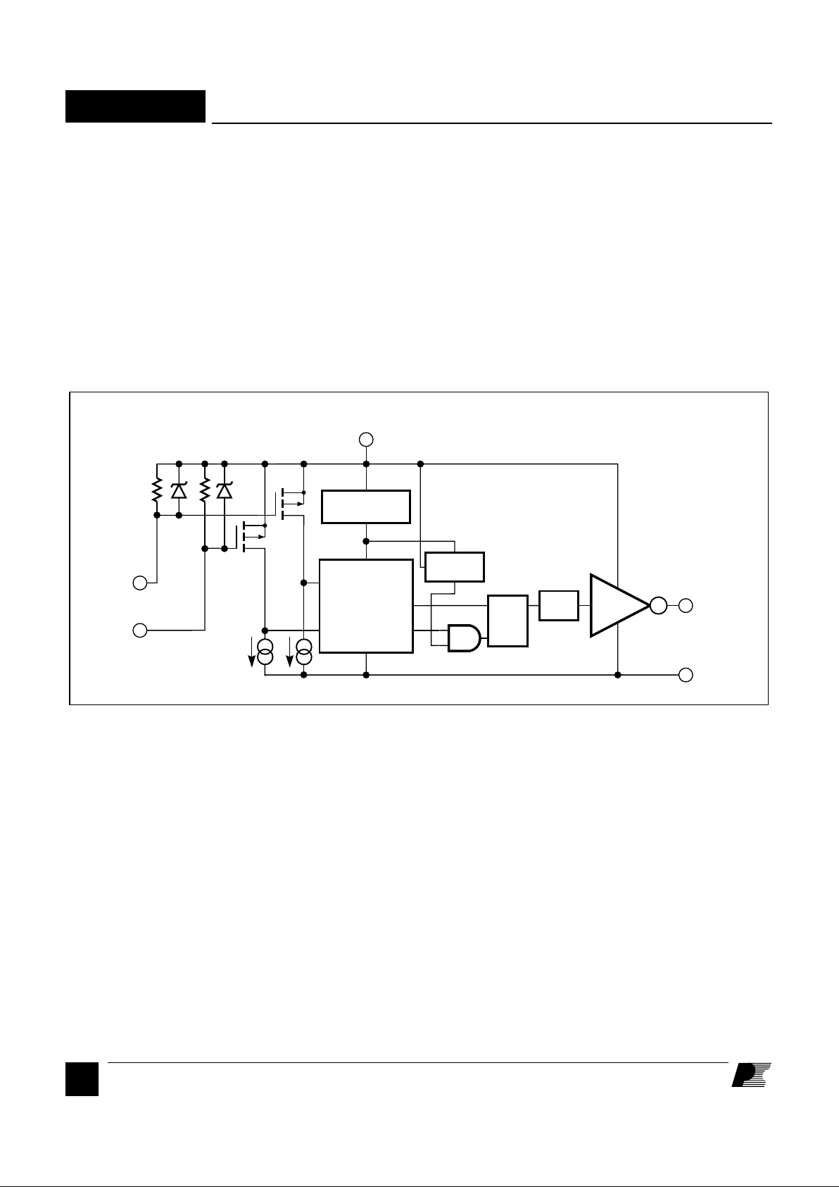
INT201 Functional Description
5 V Regulator
The 5 V linear regulator circuit provides
the supply voltage for the noise rejection
circuitry and control logic. This allows
the logic section and the driver circuitry
to be directly compatible with 5 V CMOS
logic without the need of an external 5 V
supply.
Undervoltage Lockout
The undervoltage lockout circuit disables
the HS OUT pin whenever the V
DDH
power supply falls below 9.0 V, and
maintains this condition until the V
DDH
power supply rises above 9.35 V. This
guarantees that the high side MOSFET
will be off during power-up or fault
conditions.
Noise Immunization Circuit
This circuit provides noise immunity by
combining a sampling circuit with a
flip-flop to turn on and off the driver
only when required to and not when
there is noise on the HSD inputs.
Driver
The CMOS driver circuit provides drive
power to the gate of the MOSFET used
on the high side of the half bridge circuit.
The driver consists of a CMOS buffer
capable of driving external transistors at
up to 15 V. The SOURCE pin is
connected to the source of the external
MOSFET to establish a reference for the
gate voltage.
Figure 3. Functional Block Diagram of the INT201.
HSD1
HSD2
V
DDH
SOURCE
PI-514B-021792
HS OUT
LINEAR
REGULATOR
UV
LOCKOUT
DISCRIMINATOR
DELAY
R
QS
F
2/96
INT201
3
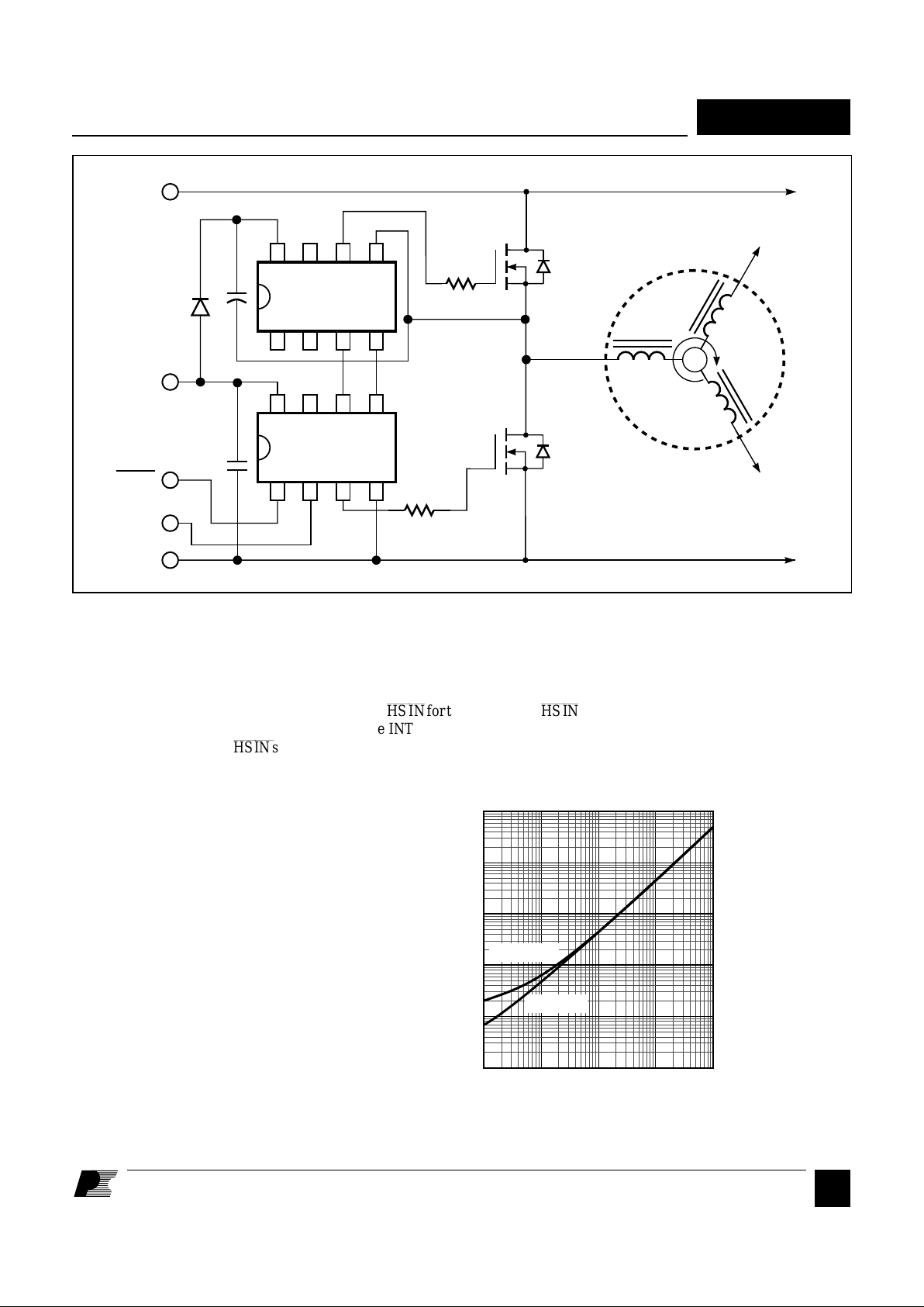
Figure 4. Using the INT200 and INT201 in a 3-phase Configuration.
General Circuit Operation
One phase of a three-phase brushless
DC motor drive circuit is shown in Figure
4 to illustrate an application of the
INT200/201. The LS IN signal directly
controls MOSFET Q1. The
HS IN
signal
causes the INT200 to command the
INT201 to turn MOSFET Q2 on or off as
required. The INT200 will ignore input
signals that would command both Q1
and Q2 to conduct simultaneously,
protecting against shorting the HV+ bus
to HV-.
Local bypassing for the low-side driver
is provided by C1. Bootstrap bias for the
high-side driver is provided by D1 and
C2. Slew rate and effects of parasitic
oscillations in the load waveforms are
controlled by resistors R1 and R2.
The inputs are designed to be compatible
with 5 V CMOS logic levels and should
not be connected to VDD. Normal CMOS
power supply sequencing should be
observed. The order of signal application
should be VDD, logic signals, and then
HV+.
The INT201 is latched on and off by the
edges of the appropriate low-side logic
signal (
HS IN
for the INT200 and
HS IN
for the INT202). The high-side driver
will latch off and stay off if the bootstrap
capacitor discharges below the
undervoltage lockout threshold.
Undervoltage lockout-induced turn off
can occur during conditions such as
power ramp up, motor start, or low speed
operation.
Figure 5. High-side On Time versus Bootstrap Capacitor.
PI-1467-042695
HV+
V
DD
LS IN
HV-
INT201
INT200
PHASE 1
PHASE 2
PHASE 3
3-PHASE
BRUSHLESS
DC MOTOR
D1
C1
C2
R1
R2
Q2
Q1
HS IN
1234
8765
1234
8765
1000
0.1
0.01
0.01 0.1 1 10 100
High Side ON Time (ms)
Bootstrap Capacitance (µF)
C
BOOTSTRAP
vs. ON TIME
1
100
PI-566B-030692
10
QG = 20 nC
QG = 100 nC
INT201
F
2/96
4
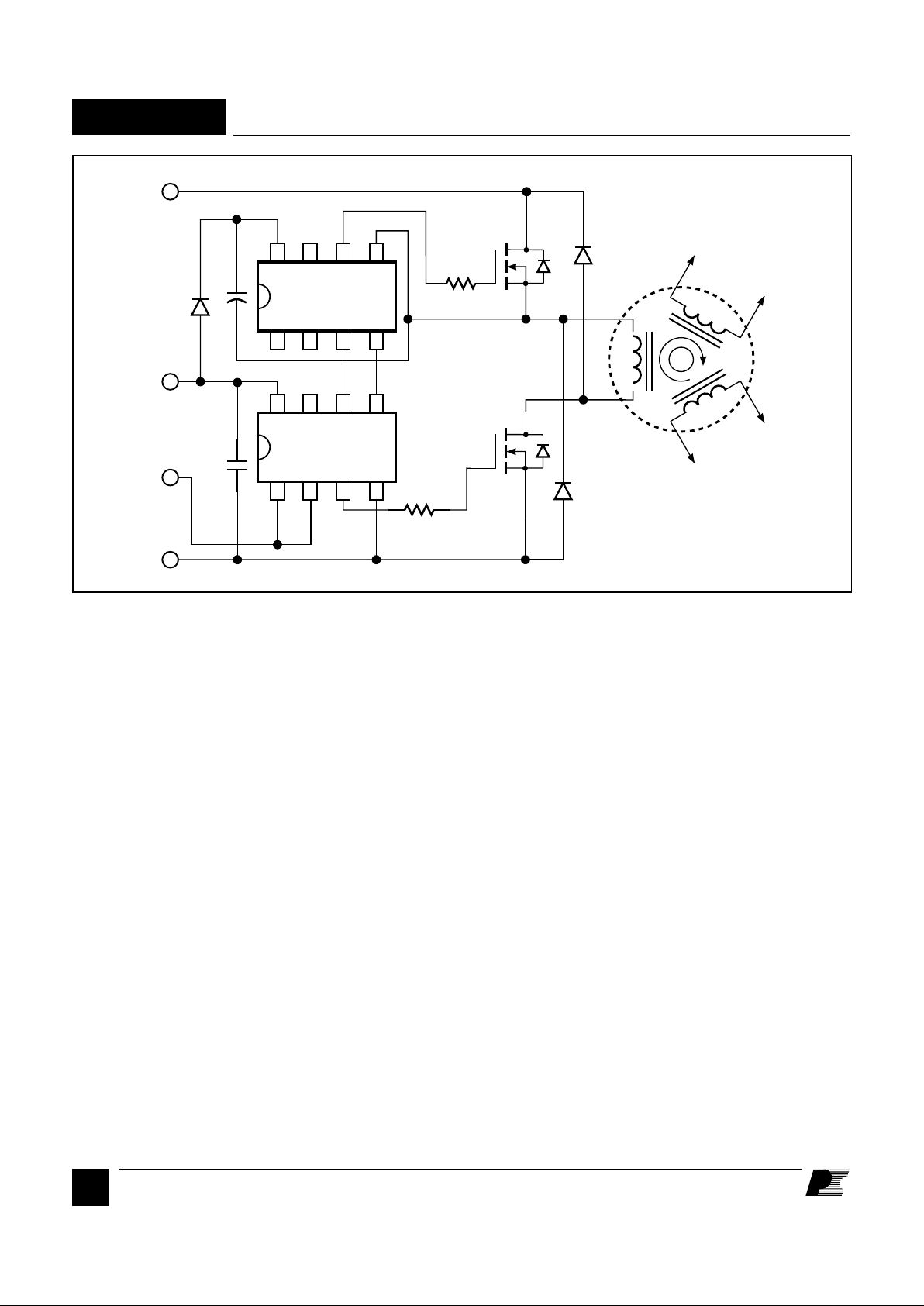
Figure 6. Using the INT202 and INT201 to Drive a Switched Reluctance Motor.
General Circuit Operation (cont.)
The bootstrap capacitor must be large
enough to provide bias current over the
entire on time interval of the high-side
driver without significant voltage sag or
decay. The MOSFET gate charge must
also be supplied at the desired switching
frequency. Figure 5 shows the maximum
high-side on time versus gate charge of
the external MOSFET. Applications
with extremely long high-side on times
require special techniques discussed in
AN-10.
A three-phase switched reluctance motor
example using the INT202/201 is given
in Figure 6. The LS IN signal directly
controls MOSFET Q1. Unlike the
INT200, the INT202 allows both the
low and high-side drivers to be on at the
same time, as this is required in
applications where the load is placed
between the low and high-side output
MOSFETs.
PI-1468-042695
HV+
V
DD
CONTROL
HV-
1234
8765
1234
8765
INT201
INT202
PHASE 1
PHASE 2
PHASE 3
3-PHASE
SRM
D1
C2
C1
R1
R2
D2
D3
Q2
Q1

F
2/96
INT201
5
Input Current
Threshold
Output Voltage,
High
Output Voltage,
Low
Output Short
Circuit Current
Turn-on
Delay Time
Rise
Time
Turn-off
Delay Time
Fall
Time
I
HSD1
, I
HSD2
V
OH
V
OL
I
OS
t
d(on)
t
r
t
d(off)
t
f
Io= -20 mA
Io= 40 mA
VO= 0 V
See Note 1
VO= V
DDH
See Figure 7
See Figure 7
See Figure 7
See Figure 7
mA
V
V
mA
µs
ns
ns
ns
-5 -2.5
V
DDH
-1.0 V
DDH
-0.5
0.3 1.0
-150
300
1.0 1.5
80 120
420 600
50 100
HSD INPUTS
HS OUT
ABSOLUTE MAXIMUM RATINGS
1
V
DDH
Voltage ............................................................16.5 V
Logic Input Voltage ................................... -0.3 V to 5.5 V
HS OUT Voltage............................ -0.3 V to V
DDH
+ 0.3 V
Storage Temperature ..................................... –65 to 125°C
Ambient Temperature ......................................-40 to 85°C
Junction Temperature............................................... 150°C
Lead Temperature
(2)
. ................................................ 260°C
Power Dissipation
PF Suffix (TA = 25˚C) ..........................................1.25 W
PF Suffix (TA = 70˚C) ........................................800 mW
TF Suffix (TA = 25˚C) ..........................................1.04 W
TF Suffix (TA = 70˚C) ........................................667 mW
Thermal Impedance (θJA)
PF Suffix ............................................................. 100°C/W
TF Suffix ............................................................. 120°C/W
1. Unless noted, all voltages referenced to SOURCE,
TA = 25˚C
2. 1/16" from case for 5 seconds.
Conditions
Parameter Symbol
(Unless Otherwise Specified) Min Typ Max Units
V
DDH
= 15 V, SOURCE = 0V
TA = -40 to 85°C

INT201
F
2/96
6
0 450
0 300
0.3 1.0
0.3 1.0
8.5 9.0 10
175 350
1.5 3.0
10 16
Dt
P+
Dt
P-
Mt
P+
Mt
P-
V
DDH(UV)
I
DDH
V
DDH
Deadtime (Low Off
to High On)
Deadtime (Low On
to High Off)
Matching (Low On
to High On)
Matching (Low Off
to High Off)
Input UV
Threshold Voltage
Input UV
Hysteresis
Supply
Current
Supply
Voltage
ns
ns
µs
µs
V
mV
mA
V
NOTES:
1. Applying a short circuit to the HS OUT pin for more than 500 µs will exceed the thermal rating of the package,
resulting in destruction of the part.
SYSTEM RESPONSE
UNDERVOLTAGE LOCKOUT
SUPPLY
See Figure 8
See Figure 8
See Figure 9
See Figure 9
Conditions
Parameter Symbol
(Unless Otherwise Specified) Min Typ Max Units
V
DDH
= 15 V, SOURCE = 0V
TA = -40 to 85°C

F
2/96
INT201
7
Figure 9. Matching Test Circuit.
Figure 8. Dead Time Test Circuit.
Figure 7. Switching Time Test Circuit.
PI-1469-042695
15 V
1234
8765
1234
8765
INT201
INT200
47 µF
35 V
0.1 µF
1000 pF
50%
0 V
INPUT
HS OUT
t
d(on)
5 V
15 V
0 V
10%
90%
10%
90%
t
f
50%
t
r
t
d(off)
PI-1470-042695
15 V
1234
8765
1234
8765
INT201
INT200
47 µF
35 V
0.1 µF
1000 pF
1000 pF
0 V
INPUT
LS OUT
Dt
p+
5 V
15 V
0 V
50%
50%
HS OUT
15 V
0 V
Dt
p-
50%
50%
PI-1471-042695
15 V
1234
8765
1234
8765
INT201
INT202
47 µF
35 V
0.1 µF
1000 pF
1000 pF
0 V
INPUT
LS OUT
Mt
p-
5 V
15 V
0 V
50%
50%
HS OUT
15 V
0 V
Mt
p+
50%
50%

INT201
F
2/96
8
1.5
0
0 25 50 75 100 125 150
Junction Temperature (°C)
Power Dissipation (W)
0.5
1.0
PACKAGE POWER DERATING
PF Suffix
TF Suffix
PI-1763-013196

F
2/96
INT201
9
PI-1842-050196
58
41
A
H
G
F
B
E
L
K
J
0 – 15
°
D
C
Dim. inches mm
A .395 MAX 10.03 MAX
B .090-.110 2.29-2.79
C .015-.021 0.38-0.53
D .040 TYP 1.02 TYP
E .015-.030 0.38-0.76
F .125 MIN 3.18 MIN
G .015 MIN 0.38 MIN
H .125-.135 3.18-3.43
J .300-.320 7.62-8.13
K .245-.255 6.22-6.48
L .009-.015 0.23-0.38
(4)
(3)
(3)
Notes:
1. Package dimensions conform to JEDEC
specification MS-001-AB for standard dual inline (DIP) package .300 inch row spacing
(PLASTIC) 8 leads (issue B, 7/85).
2. Controlling dimensions: inches.
3. Dimensions are for the molded body and do
not include mold flash or other protrusions.
Mold flash or protrusions shall not exceed .010
inch (.25 mm) on any side.
4. These dimensions measured with the leads
constrained to be perpendicular to package
bottom.
5. Pin 1 orientation identified by end notch or
dot adjacent to Pin 1.
Note 5
P08A Plastic DIP-8
PI-1845-050196
1
A
H
C
D
4
B
F
0-8˚ TYP.
J
K
85
E
G
DIM
A
B
C
D
E
F
G
H
J
K
inches
0.189-0.197
0.050 TYP
0.014-0.019
0.012 TYP
0.053-0.069
0.004-0.010
0.228-0.244
0.007-0.010
0.021-0.045
0.150-0.157
mm
4.80-5.00
1.27 TYP
0.35-0.49
0.31 TYP
1.35-1.75
0.10-0.25
5.80-6.20
0.19-0.25
0.51-1.14
3.80-4.00
Notes:
1. Package dimensions conform to JEDEC
specification MS-012-AA for standard small
outline (SO) package, 8 leads, 3.75 mm
(.150 inch) body width (issue A, June 1985).
2. Controlling dimensions are in mm.
3. Dimensions are for the molded body
and do not include mold flash or
protrusions. Mold flash or protrusions
shall not exceed .15 mm (.006 inch) on any
side.
4. Pin 1 side identified edge by chamfer on
top of the package body or indent on Pin 1
end.
(3)
(3)
T08A Plastic SO-8

INT201
F
2/96
10
Notes

F
2/96
INT201
11
Notes

INT201
F
2/96
12
JAPAN
Power Integrations, K.K.
Keihin-Tatemono 1st Bldg.
12-20 Shin-Yokohoma 2-Chome, Kohoku-ku
Yokohama-shi, Kanagawa 222 Japan
Phone: 81•(0)•45•471•1021
Fax: 81•(0)•45•471•3717
ASIA & OCEANIA
For Your Nearest Sales/Rep Office
Please Contact Customer Service
Phone: 408•523•9265
Fax: 408•523•9365
WORLD HEADQUARTERS
Power Integrations, Inc.
477 N. Mathilda Avenue
Sunnyvale, CA 94086
USA
Main: 408•523•9200
Customer Service:
Phone: 408•523•9265
Fax: 408•523•9365
AMERICAS
For Your Nearest Sales/Rep Office
Please Contact Customer Service
Phone: 408•523•9265
Fax: 408•523•9365
Power Integrations reserves the right to make changes to its products at any time to improve reliability or manufacturability.
Power Integrations does not assume any liability arising from the use of any device or circuit described herein, nor does it
convey any license under its patent rights or the rights of others.
PI Logo and
TOPSwitch
are registered trademarks of Power Integrations, Inc.
©Copyright 1994, Power Integrations, Inc. 477 N. Mathilda Avenue, Sunnyvale, CA 94086
APPLICATIONS HOTLINE
World Wide 408•523•9260
APPLICATIONS FAX
Americas 408•523•9361
Europe/Africa
44•(0)•1753•622•209
Japan 81•(0)•45•471•3717
Asia/Oceania 408•523•9364
EUROPE & AFRICA
Power Integrations (Europe) Ltd.
Mountbatten House
Fairacres
Windsor SL4 4LE
United Kingdom
Phone: 44•(0)•1753•622•208
Fax: 44•(0)•1753•622•209
 Loading...