

V
OUT
V
DD
V
REF
4~5mV
+
+
-
-
2-STEP PFM
CONTROLLED OSC
100/155kHz
VLX LIMITER
BUFFER
V
SS
L
X
EXT
CE
CHIP ENABLE
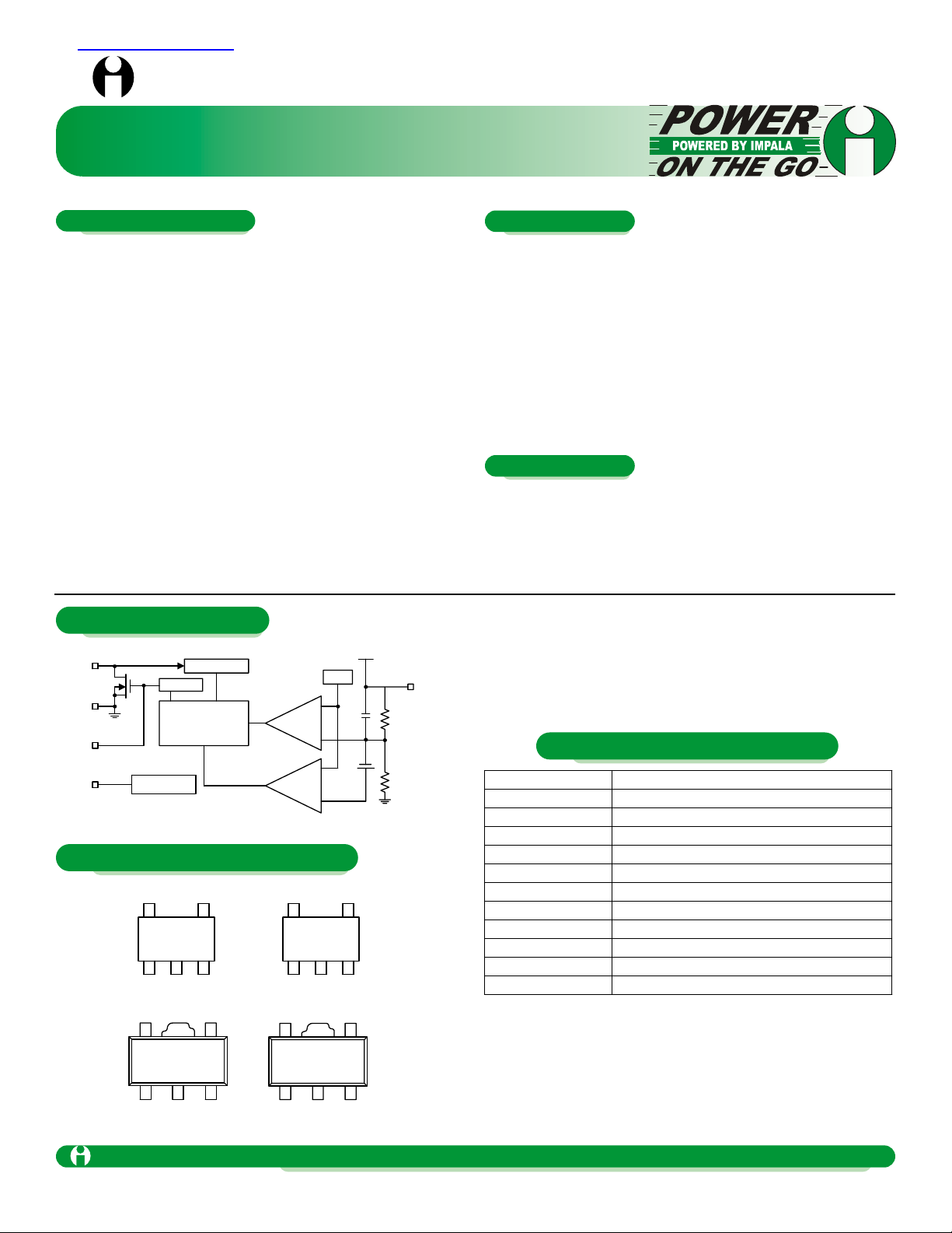
50 mA boost converter using Pulse Frequency Modulation,
or PFM, technique, in 5-lead SOT-89 or a 5-lead SOT-23
package. Only 3 external components are needed to complete the switcher design.
The ILC6390 automatically senses load variations to choose
between 55% and 75% duty cycles. Normal operation is 55%
duty at 155kHz; when load currents exceed the internal comparator trip point, a “turbo mode” kicks in to provide extended on-time switching (75% duty at 100kHz oscillation).
Requiring only 30µA of supply current, the ILC6390
achieves efficiencies as high as 85% at 5V yet shuts down
to 0.5µA max.
Standard voltages offered are 2.5, 3.3, and 5.0V and is
available in both a 5 lead SOT-23 and 5 lead SOT-89 package for small footprint applications.
In addition, the ILC6391 is configured to drive an external
transistor to achieve higher power levels.
ILC6390/91
SOT-89 Step-Up PFM Switcher
with Auto-Load Sense
Impala Linear Cor poration
Impala Linear Corporation
1
(408) 574-3939
www.impalalinear.com
Feb 2001
ILC6390 1.1
• 85% conversion efficiency at 50mA out
• Start-up voltages as low as 900mV
• ±2.5% accurate outputs
• Complete switch design with only 3 external components
• Automatically senses load variations to select the optimal
duty cycle and extend conversion efficiencyover a wide
range
• External transistor configuration to run as switcher
controller
• Shutdown to 0.5µA
• Cellular phones, pagers
• Cameras, video recorders
• Palmtops and PDAs
ILC6390CM
ILC6390CP
54
123
SOT-25
(TOP VIEW)
L
X
V
SS
CE VDDN/C
V
SS
L
X
SOT-89-5
(TOP VIEW)
54
123
N/C V
OUT
CE
ILC6391CM
54
123
SOT-25
(TOP VIEW)
L
X
V
SS
CE VDDN/C
ILC6391CP
V
SS
L
X
SOT-89-5
(TOP VIEW)
54
123
N/C V
OUT
CE
Block Diagram
Pin-Package Configurations
ILC6390CM-25
2.5V ± 2.5%
ILC6390CM-33
3.3V ± 2.5%
ILC6390CM-50
5.0V ± 2.5%
ILC6391CM-25
3.3V ± 2.5% driving external transistor
ILC6391CM-33
3.3V ± 2.5% driving external transistor
ILC6391CM-50
5.0V ± 2.5% driving external transistor
ILC6390CP-25
2.5V ± 2.5%
ILC6390CP-33
3.3V ± 2.5%
ILC6390CP-50
5.0V ± 2.5%
ILC6391CP-25
3.3V ± 2.5% driving external transistor
ILC6391CP-33
3.3V ± 2.5% driving external transistor
ILC6391CP-50
5.0V ± 2.5% driving external transistor
* Standard product offering comes in tape & reel, quantity 3000 per
reel, orientation right for SOT-25, quantity 1000 per reel orientation
right for SOT-89.
General Description Features
Applications
Ordering Information
查询ILC6390供应商查询ILC6390供应商
SOT-89 Step-Up PFM Switcher with Auto-Load Sense
Impala Linear Corporation
2
(408) 574-3939
www.impalalinear.com
Feb 2001
ILC6390 1.1
Parameter
Symbol
Ratings
Units
V
OUT
Input Voltage
V
OUT
12
V
Voltage on pin L
X
VLX 12
V
Current on pin L
X
ILX 400
mA
Voltage on pin EXT
V
EXT
VSS-0.3~V
OUT
+0.3
V
Current on pin EXT
I
EXT
±50
mA
CE Input Voltage
V
CE
12
V
V
DD
Input Voltage
V
DD
12
V
Continuous Total Power Dissipation
PD (SOT-25)
P
D
(SOT-89)
150
500
mW
Operating Ambient Temperature
T
opr
-30~+80
°C
Storage Temperature
T
stg
-40~+125
°C
Parameter
Symbol
Conditions
Min
Typ
Max
Units
Output Voltage
V
OUT
Test Circuit of Figure 1
4.875
5.000
5.125
V
Input Voltage
V
IN
10
V
Oscillation Startup Voltage
V
ST
I
OUT
= 1mA
0.80
0.9
V
Oscillation Hold Voltage
V
HLD
I
OUT
= 1mA
0.70
V
NO-Load Input Current
I
IN
I
OUT
= 0mA (See Note 1)
5.3
10.6
µA
Supply Current 1 (See Note 2)
IDD 1
V
OUT
= 4.75V
31.7
63.4
µA
Supply Current 2
IDD 2
V
OUT
= 5.5V
2.4
4.8
µA
LX Switch-On Resistance
R
SWON
V
OUT
= 4.75V, VLX = 0.4
2.8
4.3
Ω
LX Leakage Current
I
LXL
No external components, V
OUT
=
VL
X
= 10V
1.0
µA
Duty Ratio 1
DUTY 1
V
OUT
= 4.75V, Measuring of LX
waveform
70
75
80
%
Duty Ratio 2
DUTY 2
V
OUT
= 4.75V, Measuring of LX
on-time
50
55
60
%
Maximum Oscillation Freq. 1
MFO 1
V
OUT
= 4.75V, 75% duty
85
100
115
kHz
Maximum Oscillation Freq. 2
MFO 2
V
OUT
= 4.75V, 55% duty
153
180
207
kHz
Stand = by Current
I
STB
V
OUT
= 4.75V
0.5
µA
CE “High” Voltage
V
CEH
V
OUT
= 4.75V, Existance of LX
Oscillation
0.75
V
CE “Low” Voltage
V
CEL
V
OUT
= 4.75V, Disappearance of
L
X
Oscillation
0.20
V
CE “High” Current
I
CEH
VCE = V
OUT
x 0.95
0.25
µA
CE “Low” Current
I
CEL
V
OUT
= 4.75V, VCE = 0V
-0.25
µA
LX Limit Voltage
V
LXLMT
V
OUT
= 4.75V, fosc > MFO x 2
(See Note 3)
0.7 1.1
V
Note:
1. The Schottky diode (S.D.), in figure 3 must be type MA735, with Reverse current (IR) < 1.0µA at reverse voltage (VR)=10.0V
2. “Supply Current 1” is the supply current while the oscillator is continuously oscillating. In actual operation the oscillator periodically operates which
results in less average power consumption.
The current that is actually provided by external V
IN
source is represented by “No-Load Input Current”
3. The switching frequency is determined by the delay time of the internal comparator and MFO1, which sets the min. on-time
Absolute Maximum Ratings (TA= 25°C)
Electrical Characteristics ILC6390
V
OUT
= 5.0V TA= 25°C. Unless otherwise specified, VIN= V
OUT
x 0.6, I
OUT
= 50mA. See schematic, fig. 3.
SOT-89 Step-Up PFM Switcher with Auto-Load Sense
Impala Linear Corporation
3
(408) 574-3939
www.impalalinear.com
Feb 2001
ILC6390 1.1
Parameter
Symbol
Conditions
Min
Typ
Max
Units
Output Voltage
V
OUT
Test Circuit of Figure 4
4.875
5.000
5.125
V
Input Voltage
V
IN
10
V
Operation Startup Voltage
V
ST
I
OUT
= 1mA
0.80
0.9
V
Operation Hold Voltage
V
ST
I
OUT
= 1mA
0.70
V
Supply Current 1 (See Note 1)
IDD 1
V
OUT
= 4.75V
31.7
63.4
µA
Supply Current 2
IDD 2
V
OUT
= 5.5V
2.4
4.8
µA
EXT “High” On-Resistance
R
EXTH
V
OUT
= 4.75V, V
EXT
= V
OUT
-0.4
50
75
Ω
EXT “Low” On-Resistance
R
EXTL
V
OUT
= 4.75V, V
EXT
= 0.4
50
75
Ω
Duty Ratio 1
DUTY 1
V
OUT
= 4.75V, Measuring of
EXT waveform
70
75
80
%
Duty Ratio 2
DUTY 2
VIN = V
OUT
x 0.95, I
OUT
= 1mA,
Measuring of EXT High State
50
55
60
%
Maximum Oscillation Freq. 1
MFO 1
V
OUT
= 4.75V, 75% duty
85
100
115
kHz
Maximum Oscillation Freq. 2
MFO 2
VIN = V
OUT
x 0.95, 55% duty
153
180
207
kHz
Stand = by Current
I
STB
V
OUT
= 4.75V
0.5
µA
CE “High” Voltage
V
CEH
V
OUT
= 4.75V, Existence of
EXT Oscillation
0.75
V
CE “Low” Voltage
V
CEL
V
OUT
= 4.75V, Disappearance
of EXT Oscillation
0.20
V
CE “High” Current
I
CEH
VCE = V
OUT
= 4.75V
0.25
µA
CE “Low” Current
I
CEL
V
OUT
= 4.75V, V
CE
= 0V
-0.25
µA
Efficiency
EFFI
Test Circuit Figure 4
85 %
Note:
1. “Supply Current 1” is the supply current while the oscillator is continuously oscillating. In actual operation the oscillator periodically operates
which results in less average power consumption.
Electrical Characteristics ILC6391
V
OUT
= 5.0V TA = 25°C. Unless otherwise specified, V
IN
= V
OUT
x 0.6, I
OUT
= 50mA. See schematic, Fig.4

SOT-89 Step-Up PFM Switcher with Auto-Load Sense
Impala Linear Corporation
4
(408) 574-3939
www.impalalinear.com
Feb 2001
ILC6390 1.1
2
ILC6390CM
13
13
L
V
IN
GND
CE
SD
+
C
L
V
OUT
ILC6391CP
123
45
CE
V
OUT
C
L
+
L
SD
V
IN
GND
C
B
R
B
Tr
ILC6391CM
123
45
CE
V
OUT
C
L
+
L
SD
V
IN
GND
R
Tr
ILC6390CP
123
45
CE
V
OUT
C
L
+
L
SD
V
IN
GND
L: 100µH (SUMIDA, CD-54
SD: Diode (Schottky diode; MATSUSHITA MA 735)
CL: 16V 47µF (Tantalum Capacitor; NICHICON, f93)
L: 47µH (SUMIDA, CD-54)
SD: Diode (Schottky diode; MATSUSHITA MA735)
C
L
: 16V 47µF (Tantalum Capacitor; NICHICON, F93)
R
B
: 1kΩ
CB: 3300pF
Tr: 2SC3279, 2SDI628G
Parameter
Efficiency
Symbol
EFFI
Conditions
Test Circuit of Figure 3
Units
%
MaxTyp
85
Min
Application Circuits
Electrical Characteristics ILC6390
V
OUT
= 5.0V TA= 25°C. Unless otherwise specified, VIN= V
OUT
x 0.6, I
OUT
= 50mA. See schematic, fig. 3.

SOT-89 Step-Up PFM Switcher with Auto-Load Sense
Impala Linear Corporation
5
(408) 574-3939
www.impalalinear.com
Feb 2001
ILC6390 1.1
The ILC6390 performs boost DC-DC conversion by controlling the
switch element shown in the circuit below.
When the switch is closed, current is built up through the inductor.
When the switch opens, this current has to go somewhere and is
forced through the diode to the output. As this on and off switching continues, the output capacitor voltage builds up due to the
charge it is storing from the inductor current. In this way, the output voltage gets boosted relative to the input. The ILC6390 monitors the voltage on the output capacitor to determine how much
and how often to drive the switch.
In general, the switching characteristic is determined by the output
voltage desired and the current required by the load. Specifically
the energy transfer is determined by the power stored in the coil
during each switching cycle.
P
L
= ƒ(tON, VIN)
The ILC6390 and ILC6391 use a PFM or Pulse Frequency
Modulation technique. In this technique, the switch is always
turned on for a fixed period of time, corresponding to a fixed
switching frequency at a predefined duty cycle. For the ILC6390
this value is 3.55msec on time, corresponding to 55% duty cycle
at 155kHz. Because the inductor value, capacitor size, and
switch on-time and frequency are all fixed, the ILC6390 in essence
delivers the same amount of power to the output during each
switching cycle. This in turn creates a constant output voltage
ramp which is dependent on the output load requirement. In this
mode, the only difference between the PFM and PWM techniques
is the duty cycle of the switch.
Once the output voltage reaches the set point, the ILC6390 will
shut off the switch oscillator and wait until the output voltage
drops low again, at which point it will re-start the oscillator. As
you can see in the diagram, the PFM boost converter actually
skips pulses as a way of varying the amount of power being delivered to the output.
Because of this, PFM is sometimes called “Pulse Skipping
Modulation.”
The chief advantage of using a PFM technique is that, at low currents, the switcher is able to maintain regulation without constantly driving a switch on and off. This power savings can be
5mA or more for the ILC6390 versus the ILC6370, and at very
light loads this current difference can make a noticeable impact
on overall efficiency.
However, because the ILC6390 will skip pulses based on
load current, the effective frequency of switching may well
drop into the audio band. This means that the radiated
noise of the ILC6390 may interfere with the audio channel
of the system and additional filtering may be necessary. In
addition, because the PFM on-time is fixed, it usually has
higher output ripple voltage than the PWM switcher, which
dynamically changes the on-time to match the load current
requirements. [Ripple is due to the output cap constantly
accepting and storing the charge received from the inductor, and delivering charge as required by the load. The
“pumping” action of the switch produces a sawtoothshaped voltage as seen by the output.]
On the plus side, because pulses are skipped, overtone content of
the frequency noise is lower than in a PWM configuration. The
sum of these characteristics for PFM converters makes it the ideal
choice for low-current or ultra-long runtime applications, where
overall conversion efficiency at low currents is of primary concern.
[For other conversion techniques, please see the ILC6370/71 and
ILC6380/81 datasheets.]
Dual-Step Mode
The ILC6390 and ILC6391 have one other unique feature, that
being to automatically switch to a second switching scheme in the
presence of heavy output loading. As we mentioned, the standard switching scheme for these parts is a 3.55msec, 155kHz,
55% duty cycle part. However, if the device detects that the output load increases beyond a set point (as seen by the voltage
drop on the output capacitor), it switches in a 7.5msec, 100kHz,
75% duty cycle “turbo mode” specifically to keep up with the
increased load demand. This switchover is seamless to the user,
but will result in a change in the output ripple voltage characteristic of the DC-DC converter.
PFM converters are widely used in portable consumer applications not requiring a high current level and relatively unaffected by
audio noise. Applications such as pagers and PDAs, which need
to operate in stand-by for extended periods of time, gravitate
toward the advantages of PFM since maximum run-time is a chief
differentiating element. The ILC6390 addresses this low-current
requirement, and additionally offers a “turbo” mode which maintains output regulation in the presence of heavier-than-normal
load currents, and maintains 0.5mA shutdown currents.
The only difference between the ILC6390 and ILC6391 parts is
that the 6391 is configured to drive an external transistor as the
switch element. Since larger transistors can be selected for this
element, higher effective loads can be regulated.
V
SET
V
OUT
Switch Waveform

SOT-89 Step-Up PFM Switcher with Auto-Load Sense
Impala Linear Corporation
6
(408) 574-3939
www.impalalinear.com
Feb 2001
ILC6390 1.1
External Components and Layout Consideration
The ILC6390 is designed to provide a complete DC-DC converter
solution with a minimum of external components. Ideally, only
three externals are required: the inductor, a pass diode, and an
output capacitor.
The inductor needs to be of low DC Resistance type, typically 1Ω
value. Toroidal wound inductors have better field containment (less
high frequency noise radiated out) but tend to be more expensive.
Some manufacturers like Coilcraft have new bobbin-wound inductors with shielding included, which may be an ideal fit for these
applications. Contact the manufacturer for more information.
The inductor size needs to be in the range of 47mH to 1mH. In
general, larger inductor sizes deliver less current, so the load current will determine the inductor size used.
For load currents higher than 10mA, use an inductor from 47mH
to 100mH. [The 100mH inductor shown in the datasheet is the
most typical used for this application.]
For load currents of around 5mA, such as pagers, use an inductor
in the range of 100mH to 330mH. 220mH is the most typical value
used here.
For lighter loads, an inductor of up to 1mH can be used. The use
of a larger inductor will increase overall conversion efficiency, due
to the reduction in switching currents through the device.
For the ILC6391, using an external transistor, the use of a 47mH
inductor is recommended based on our experience with the part.
The capacitor should, in general, always be tantalum type, as tantalum has much better ESR and temperature stability than other
capacitor types. NEVER use electrolytics or chemical caps, as the
C-value changes below 0×C so much as to make the overall
design unstable.
Different C-values will directly impact the ripple seen on the output
at a given load current, due to the direct charge-to-voltage relationship of this element. Different C-values will also indirectly affect
system reliability, as the lifetime of the capacitor can be degraded
by constant high current influx and outflux. Running a capacitor
near its maximum rated voltage can deteriorate lifetime as well;
this is especially true for tantalum caps which are particularly sensitive to overvoltage conditions.
In general, then, this capacitor should always be 47mF, Tantalum,
16V rating.
The diode must be of shottkey type for fast recovery and minimal
loss. A diode rated at greater than 200mA and maximum voltage
greater than 30V is recommended for the fastest switching time
and best reliability over time. Different diodes may introduce different levels of high frequency switching noise into the output
waveform, so trying out several sources may make the most
sense for your system.
For the IL6391, much of the component selection is as described
above, with the addition of the external NPN transistor and the
base drive network. The transistor needs to be of NPN type, and
should be rated for currents of 2A or more. [This translates to
lower effective on resistance and, therefore, higher overall efficiencies.] The base components should remain at 1kΩ and
3300pF; any changes need to be verified prior to implementation.
As for actual physical component layout, in general, the more
compact the layout is, the better the overall performance will be. It
is important to remember that everything in the circuit depends on
a common and solid ground reference. Ground bounce can directly affect the output regulation and presents difficult behavior to
predict. Keeping all ground traces wide will eliminate ground
bounce problems.
It is also critical that the ground pin of C
L
and the VSSpin of the
device be the same point on the board, as this capacitor serves
two functions: that of the output load capacitor, and that of the
input supply bypass capacitor.
Layouts for DC-DC converter designs are critical for overall performance, but following these simple guidelines can simplify the
task by avoiding some of the more common mistakes made in
these cases. Once actual performance is completed, though, be
sure to double-check the design on actual manufacturing prototype product to verify that nothing has changed which can affect
the performance.

SOT-89 Step-Up PFM Switcher with Auto-Load Sense
Impala Linear Corporation
7
(408) 574-3939
www.impalalinear.com
Feb 2001
ILC6390 1.1
OUTPUT VOLTAGE vs. OUTPUT CURRENT
OUTPUT VOLTAGE vs. OUTPUT CURRENT
EFFICIENCY vs. OUTPUT CURRENT
EFFICIENCY vs. OUTPUT CURRENT
EFFICIENCY vs. OUTPUT CURRENTEFFICIENCY vs. OUTPUT CURRENT
RIPPLE VOLTAGE vs. OUTPUT CURRENT
RIPPLE VOLTAGE vs. OUTPUT CURRENT
ILC6390CP-30 ILC6390CP-50
ILC6390CP-50
ILC6390CP-50
ILC6391CP-50
ILC6390CP-30
ILC6390CP-30
ILC6391CP-30
4.0
3.5
3.0
2.5
2.0
1.5
1.0
0.5
7.
6.0
5.0
4.0
3.0
2.0
1.0
0
100
80
60
40
20
0
100
80
60
40
20
0
100
80
60
40
20
0
100
80
60
40
20
0
100
80
60
40
20
0
100
80
60
40
20
0
0 20 40 60 80 100 0 20 40 60 80 100
0 20 40 60 80 100
0 20 40 60 80 100
0 20 40 60 80 100
0 20 40 60 80 100
0 100 200 300 400 500 0 100 200 300 400 500
OUTPUT CURRENT I
OUT
(mA)
OUTPUT CURRENT I
OUT
(mA)
OUTPUT CURRENT I
OUT
(mA)
OUTPUT CURRENT I
OUT
(mA)
OUTPUT CURRENT I
OUT
(mA)
OUTPUT CURRENT I
OUT
(mA)
OUTPUT CURRENT I
OUT
(mA)
OUTPUT CURRENT I
OUT
(mA)
OUTPUT VOLTAGE V
OUT
(V)
OUTPUT VOLTAGE V
OUT
(V)
EFFICIENCY: EFFI (%)
EFFICIENCY: EFFI (%)
EFFICIENCY: EFFI (%)
EFFICIENCY: EFFI (%)
RIPPLE Vr (mV
p-p
)
RIPPLE Vr (mV
p-p
)
L = 100µH
C = 10µF(Tantalum)
L = 100µH
C = 10µF(Tantalum)
L = 100µH
C = 10µF(Tantalum)
L = 100µH
C = 10µF(Tantalum)
L = 100µH
C = 10µF(Tantalum)
L = 100µH
C = 10µF(Tantalum)
V
IN
= 0.9V
V
IN
= 0.9V
V
IN
= 0.9V
V
IN
= 0.9V
V
IN
= 0.9V
V
IN
= 1.2V
V
IN
= 1.2V
V
IN
= 1.2VV
IN
= 1.2V
V
IN
= 1.2V
V
IN
= 1.2V
V
IN
= 1.2V
V
IN
= 1.0V
V
IN
= 1.5V
V
IN
= 1.5V
V
IN
= 1.5VV
IN
= 1.5V
V
IN
= 1.5V
V
IN
= 1.5V
V
IN
= 1.8V
V
IN
= 1.5V
V
IN
= 1.5V
V
IN
= 1.8V
V
IN
= 1.8V
V
IN
= 2.0V
V
IN
= 2.0V
V
IN
= 2.0V
V
IN
= 2.0V
V
IN
= 2.0V
V
IN
= 2.0V
V
IN
= 3.0V
V
IN
= 3.0V
V
IN
= 3.0V
V
IN
= 3.0V
L = 22µH (CD105)
RB= 300
CB= 0
L = 22µH (CD54)
RB= 300
CB= 0
Typical Performance Characteristics General conditions for all curves

SOT-89 Step-Up PFM Switcher with Auto-Load Sense
Impala Linear Corporation
8
(408) 574-3939
www.impalalinear.com
Feb 2001
ILC6390 1.1
OUTPUT VOLTAGE vs. OUTPUT CURRENT
EFFICIENCY vs. OUTPUT CURRENT
EFFICIENCY vs. OUTPUT CURRENT
OUTPUT VOLTAGE vs. OUTPUT CURRENT
OUTPUT VOLTAGE vs. OUTPUT CURRENT
OUTPUT VOLTAGE vs. OUTPUT CURRENT
ILC6391CP-30
ILC6391CP-30
ILC6391CP-30
ILC6391CP-30
OUTPUT VOLTAGE V
OUT
(V)
OUTPUT VOLTAGE V
OUT
(V)
OUTPUT VOLTAGE V
OUT
(V)
OUTPUT VOLTAGE V
OUT
(V)
ILC6391CP-50
ILC6391CP-50
ILC6391CP-50
ILC6391CP-50
RIPPLE VOLTAGE vs. OUTPUT CURRENTRIPPLE VOLTAGE vs. OUTPUT CURRENT
RIPPLE Vr (mV
p-p
)
RIPPLE Vr (mV
p-p
)
L = 22µH (CD105)
RB= 300
CB= 0.1µF
L = 22µH (CD105)
RB= 300
CB= 0.1µF
L = 22µH (CD105)
RB= 300
CB= 0
L = 22µH (CD54)
RB= 500
CB= 0
L = 22µH (CD105)
RB= 300
CB= 0.1µF
L = 22µH (CD105)
RB= 300
CB= 0.1µF
EFFICIENCY: EFFI (%)
EFFICIENCY: EFFI (%)
7.0
6.0
5.0
4.0
3.0
2.0
1.0
0
0 100 200 300 400 500
400
300
200
100
0
OUTPUT CURRENT I
OUT
(mA)
0 20 40 60 80 100
4.0
3.5
3.0
2.5
2.0
1.5
1.0
0.5
0 100 200 300 400 500
OUTPUT CURRENT I
OUT
(mA)
500
400
300
200
100
0
0 100 200 300 400 500
OUTPUT CURRENT I
OUT
(mA)
100
80
60
40
20
0
0 200 400 600 800
OUTPUT CURRENT I
OUT
(mA)
6
5
4
3
2
1
0
0 200 400 600 800
OUTPUT CURRENT I
OUT
(mA)
OUTPUT CURRENT I
OUT
(mA)
0 20 40 60 80 100
4.0
3.5
3.0
2.5
2.0
1.5
1.0
0.5
OUTPUT CURRENT I
OUT
(mA)
100
80
60
40
20
0
0 100 200 300 400 500
OUTPUT CURRENT I
OUT
(mA)
L = 22µF (CD105)
RB= 300
CB= 0
L = 22µF (CD54)
RB= 500
CB= 0
VIN= 1.0V
VIN= 1.0V
VIN= 1.0V
VIN= 2.0V
VIN= 2.0V
VIN= 2.0V
VIN= 2.0V
VIN= 3.0V
VIN= 3.0V
VIN= 3.0V
VIN= 3.0V
VIN= 1.2V
VIN= 1.2V
VIN= 1.2V
VIN= 1.2V
VIN= 1.2V
VIN= 1.5V
VIN= 1.5V
VIN= 1.5V
VIN= 1.5V
VIN= 1.5V
VIN= 1.5V
VIN= 1.5V
VIN= 1.5V
VIN= 1.8V
VIN= 1.8V
VIN= 1.8V
VIN= 1.8V
Typical Performance Characteristics General conditions for all curves

SOT-89 Step-Up PFM Switcher with Auto-Load Sense
Impala Linear Corporation
9
(408) 574-3939
www.impalalinear.com
Feb 2001
ILC6390 1.1
RIPPLE VOLTAGE vs. OUTPUT CURRENT
RIPPLE VOLTAGE vs. OUTPUT CURRENT
ILC6391CP-30
ILC6391CP-50
0 200 400 600 800
0 200 400 600 800
400
300
200
100
0
600
500
400
300
200
100
0
RIPPLE Vr (mV
p-p
)
RIPPLE Vr (mV
p-p
)
OUTPUT CURRENT I
OUT
(mA)
L = 22µH (CD105)
RB= 300
CB= 0.1µF
L = 22µF (CD105)
RB= 300
CB= 0.1µF
VIN= 1.5V
VIN= 1.5V
VIN= 1.2V
VIN= 1.8V
VIN= 2.0V
VIN= 3.0V
OUTPUT CURRENT I
OUT
(mA)
Typical Performance Characteristics General conditions for all curves
 Loading...