

POSEICO AT866LTS36 Datasheet

Tj
From 75% VDRM up to 2400 A, gate 40V 5ohm
-30 /
standard specification
ANSALDO
Ansaldo Trasporti s.p.a.
Unita' Semiconduttori
PHASE CONTROL THYRISTOR AT866LT
Repetitive voltage up to 3600 V
Mean on-state current 2375 A
Surge current 29.1 kA
FINAL SPECIFICATION
apr 97 - ISSUE : 01
Via N. Lorenzi 8 - I 16152 GENOVA - ITALY
Tel. int. +39/(0)10 6556549 - (0)10 6556488
Fax Int. +39/(0)10 6442510
Tx 270318 ANSUSE I -
Symbol Characteristic Conditions
[°C]
Value Unit
BLOCKING
V RRM Repetitive peak reverse voltage 125 3600 V
V RSM Non-repetitive peak reverse voltage 125 3700 V
V DRM Repetitive peak off-state voltage 125 3600 V
I RRM Repetitive peak reverse current V=VRRM 125 250 mA
I DRM Repetitive peak off-state current V=VDRM 125 250 mA
CONDUCTING
I T (AV) Mean on-state current 180° sin, 50 Hz, Th=55°C, double side cooled 2375 A
I T (AV) Mean on-state current 180° sin, 50 Hz, Tc=85°C, double side cooled 1935 A
I TSM Surge on-state current sine wave, 10 ms 125 29.1 kA
I² t I² t without reverse voltage 4234 x1E3 A²s
V T On-state voltage On-state current = 2000 A 25 1.85 V
V T(TO) Threshold voltage 125 1.2 V
r T On-state slope resistance 125 0.325 mohm
SWITCHING
di/dt Critical rate of rise of on-state current, min.
dv/dt Critical rate of rise of off-state voltage, min. Linear ramp up to 70% of VDRM 125 1000 V/µs
td Gate controlled delay time, typical VD=100V, gate source 40V, 10 ohm , tr=.5 µs 25 3 µs
tq Circuit commutated turn-off time, typical dV/dt = 20 V/µs linear up to 75% VDRM 400 µs
Q rr Reverse recovery charge di/dt=-20 A/µs, I= 1570 A 125 µC
I rr Peak reverse recovery current VR= 50 V A
I H Holding current, typical VD=5V, gate open circuit 25 300 mA
I L Latching current, typical VD=12V, tp=30µs 25 1000 mA
125 200 A/µs
GATE
V GT Gate trigger voltage VD=12V 25 3.5 V
I GT Gate trigger current VD=12V 25 400 mA
V GD Non-trigger gate voltage, min. VD=VDRM 125 0.25 V
V FGM Peak gate voltage (forward) 30 V
I FGM Peak gate current 10 A
V RGM Peak gate voltage (reverse) 5 V
P GM Peak gate power dissipation Pulse width 100 µs 150 W
P G Average gate power dissipation 2 W
MOUNTING
R th(j-h) Thermal impedance, DC Junction to heatsink, double side cooled 9.5 °C/kW
R th(c-h) Thermal impedance Case to heatsink, double side cooled 2 °C/kW
T j Operating junction temperature
F Mounting force 40.0 / 50.0 kN
Mass 1150 g
ORDERING INFORMATION : AT866LT S 36
VDRM&VRRM/100
125 °C
AT866LT PHASE CONTROL THYRISTOR
ANSALDO
FINAL SPECIFICATION apr 97 - ISSUE : 01
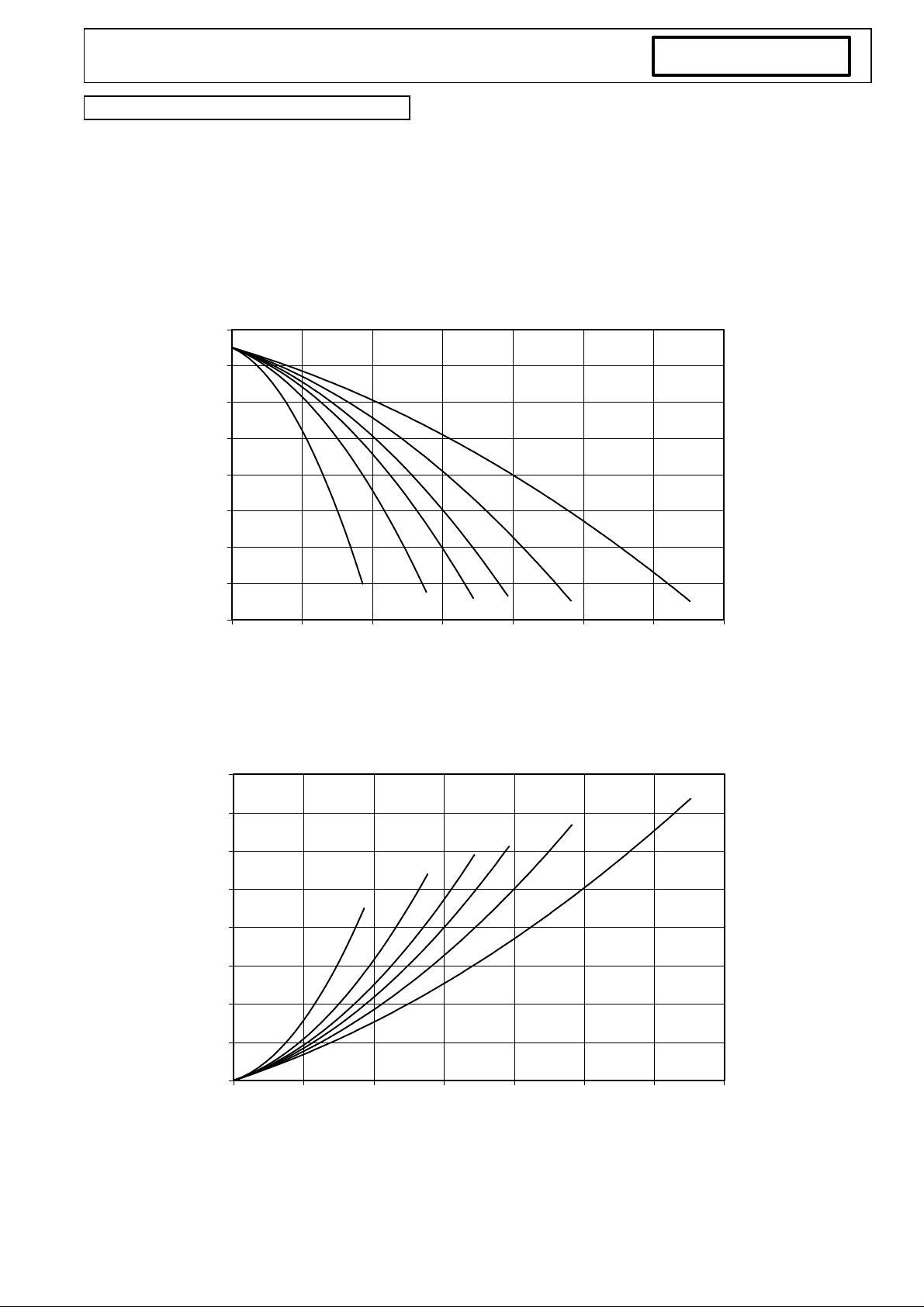
DISSIPATION CHARACTERISTICS
SQUARE WAVE
Th [°C]
130
120
110
100
90
30°
80
60°
70
90°
60
50
0 500 1000 1500 2000 2500 3000 3500
120°
180°
DC
PF(AV) [W]
8000
7000
6000
5000
4000
3000
2000
1000
0
IF(AV) [A]
120°
180°
90°
60°
30°
DC
0 500 1000 1500 2000 2500 3000 3500
IF(AV) [A]
 Loading...