

Page 1

RUBY-9712VG2A
Industrial Mainboard
User's Manual
P/N: B8980230 Version 1.0
Copyright © Portwell, Inc., 2005. All rights reserved.
All other brand names are registered trademarks of their respective owners.
Page 2

Preface
Table of Contents
How to Use This Manual
Chapter 1 System Overview.......................................................................................................1-1
1.1 Introduction.................................................................................................................................. 1-1
1.2 Check List ..................................................................................................................................... 1-2
1.3 Product Specification ..................................................................................................................1-2
1.3.1 Mechanical Drawing......................................................................................................... 1-5
1.4 System Architecture .................................................................................................................... 1-6
Chapter 2 Hardware Configuration ...........................................................................................2-1
2.1 Jumper Setting ............................................................................................................................. 2-1
2.2 Connector Allocation .................................................................................................................. 2-3
Chapter 3 System Installation....................................................................................................3-1
3.1 Pentium 4 Processor.................................................................................................................... 3-1
3.2 Main Memory .............................................................................................................................. 3-3
3.3 CompactFlash Card..................................................................................................................... 3-4
3.4 Installing the Single Board Computer ...................................................................................... 3-4
3.4.1 Chipset Component Driver.............................................................................................. 3-5
3.4.2 Intel Integrated Graphics GMCH Chip.......................................................................... 3-5
3.4.3 On-board Fast Ethernet Controller ................................................................................. 3-6
3.4.4 On-board AC-97 Audio Device....................................................................................... 3-7
3.5 Clear CMOS Operation............................................................................................................... 3-7
3.6 WDT Function.............................................................................................................................. 3-7
3.7 GPIO.............................................................................................................................................. 3-9
3.7.1 Pin assignment................................................................................................................... 3-9
3.7.2 Programming Guide ....................................................................................................... 3-10
3.7.3 Example ............................................................................................................................ 3-11
Chapter 4 BIOS Setup Information............................................................................................4-1
4.1 Entering Setup.............................................................................................................................. 4-1
4.2 Main Menu ................................................................................................................................... 4-2
4.3 Standard CMOS Setup Menu ....................................................................................................4-3
4.4 IDE Adaptors Setup Menu......................................................................................................... 4-4
4.5 Advanced BIOS Feature .............................................................................................................4-7
4.6 Advanced Chipset Feature....................................................................................................... 4-11
4.7 Integrated Peripherals .............................................................................................................. 4-14
4.8 Power Management Setup ....................................................................................................... 4-20
4.9 PnP/PCI Configurations .......................................................................................................... 4-24
4.10 PC Health Status...................................................................................................................... 4-27
4.11 Frequency/Voltage Control................................................................................................... 4-27
4.12 Default Menu ...........................................................................................................................4-28
4.13 Supervisor/User Password Setting ...................................................................................... 4-29
4.14 Exiting Selection ...................................................................................................................... 4-30
Chapter 5 Troubleshooting ........................................................................................................ 5-1
5.1 Hardware Quick Installation ..................................................................................................... 5-1
5.2 BIOS Setting.................................................................................................................................. 5-5
5.3 FAQ ............................................................................................................................................... 5-7
Appendix A
Appendix B
Page 3

Preface
How to Use This Manual
The manual describes how to configure your RUBY-9712VG2A system to meet
various operating requirements. It is divided into five chapters, with each chapter
addressing a basic concept and operation of Industrial Mainboard.
Chapter 1 : System Overview. Presents what you have in the box and give you an
overview of the product specifications and basic system architecture for this model
of Industrial Mainboard.
Chapter 2 : Hardware Configuration. Shows the definitions and locations of
Jumpers and Connectors that you can easily configure your system.
Chapter 3 : System Installation. Describes how to properly mount the CPU, main
memory and CompactFlash to get a safe installation and provides a programming
guide of Watch Dog Timer function.
Chapter 4 : BIOS Setup Information. Specifies the meaning of each setup
parameters, how to get advanced BIOS performance and update new BIOS. In
addition, POST checkpoint list will give users some guidelines of trouble-shooting.
Chapter 5 : Troubleshooting. Provides various useful tips to quickly get RUBY9712VG2A series running with success. As basic hardware installation has been
addressed in Chapter 3, this chapter will basically focus on system integration issues,
in terms of backplane setup, BIOS setting, and OS diagnostics.
The content of this manual and EC declaration document is subject to change
without prior notice. These changes will be incorporated in new editions of the
document. Portwell may make supplement or change in the products described in
this document at any time.
Updates to this manual, technical clarification, and answers to frequently asked
questions will be shown on the following web site : http://www.portwell.com/.
Page 4

Preface
EC Declaration of Conformity
(To Be Added)
For the following equipment:
Product Name:
Model Name:
Trade Name:
is herewith confirmed to comply with the requirements set out in the Council
Directive on the Approximation of the Laws of the Member States relating to
Electromagnetic Compatibility Directive (89/336/EEC). The equipment was
evaluated and passed the test, the following standards were applied :
EMC : EN 55022 (1994/A1:1995 Class A)
EN 50082-2 (1991)
EN 61000-4-2 (1995)
EN 61000-4-3 (1996)
EN 61000-4-4 (1995)
EN 61000-3-2 (1995)
EN 61000-3-3 (1995)
The following manufacturer is responsible for this declaration :
Portwell, Inc.
(Company Name)
3F, No.88, Sec.1, Nei-Hu Rd., Taipei, Taiwan, R.O.C.
(Company Address)
Taipei, R.O.C.
Place Date Legal Signature of
Authorized Person
Page 5

System Overview
RUBY-9712VG2A User’s Manual 1-1
Chapter 1
System Overview
1.1 Introduction
RUBY-9712VG2A, uATX form factor Industrial Mainboard that based on Intel’s PCI
Express chipset 915GV. The new generation chipset, 915GV and ICH6 supports
new package LGA (Land Grid Array) Pentium 4 and Celeron D processor and I/O
interconnection of PCI Express x1.
New 775-land, 90nm process processor enabled higher computing speed and also
included 13 new instructions (SSE3, Streaming SIMD Extensions 3) enhanced the
performance of optimized applications for video, image processing, media
compression and gaming. More data transactions are expected for more powerful
processor, however, traditional expansion interface, 32-bit PCI bus is not enough.
Even there is evolution of 64-bit PCI and PCI-X bus, the bandwidth still limited to its
bus architecture and add-on card number. Such parallel data transmission
technology is gradually replaced by serial. SATA is one of the examples. PCI
Express, new I/O interface solved the bandwidth bottleneck with scalable
performance and with frequency and lanes. PCI compatible configuration and
device driver interface makes the migration without extra effort. And that is the
interface of dual Gigabit Ethernet on RUBY-9712VG2A.
RUBY-9712VG2A embedded Intel Graphics Media Accelerator (GMA) 900, the thirdgeneration Graphics core delivers a better media viewing experience by fast core,
increased memory bandwidth and hardware acceleration for Microsoft DirectX 9
improves 3D performance. Beside all these wonderful things, RUBY-9712VG2A
also remains some features that dedicated for industrial applications such as 32-bit
PCI expansion, Watch Dog Timer, CompactFlash socket and GPIO.
Following is brief specification of RUBY-9712VG2A –
Micro ATX industrial mainboard based on Intel 915GV, ICH6 chipset
Support Intel latest LGA775 type Pentium 4 / Celeron D processor with
800/533MHz FSB
Two DIMM sockets support DDR 333/400 SDRAM up to 2GB memory
Four 32-bit PCI slots
Dual Gigabit Ethernet via PCI Express x1 interface
One Ultra DMA 100/66 IDE channel; one CompactFlash socket; three SATA
ports; Six USB ports; one Parallel port.
Page 6

System Overview
RUBY-9712VG2A User’s Manual 1-2
1.2 Check List
The RUBY-9712VG2A package should cover the following basic items:
One RUBY-9712VG2A Industrial Mainboard
One I/O shield
One IDE cable
One 7-pin SATA signal cable
One Installation Resources CD-Title
One booklet of RUBY-9712VG2A manual
If any of these items is damaged or missing, please contact your vendor and keep all
packing materials for future replacement and maintenance.
1.3 Product Specification
Main processor
- Intel® Pentium® 4/Celeron D Processor in LGA 775 package
- FSB: 800/533MHz
BIOS
Phoenix (Award) system BIOS with 4Mb Flash ROM with easy upgrade function
ACPI, DMI, Green function and Plug and Play Compatible
Main Memory
- Support dual-channel & signal channel DDR memory interface
- Non-ECC, non-buffered DIMMS only
- Two DIMM sockets support 333/400 DDR-SDRAM up to 2GB System Memory
L2 Cache Memory
Included in processor
Chipset
Intel 915GV GMCH/MCH and ICH6 chipset
Bus Interface
Fully complies with PCI Local Bus specification V2.3 (support 4 master PCI slots)
PCI IDE Interface
Support one enhanced IDE ports up to four HDD devices with PIO mode 4 and
Ultra DMA/33/66/100 mode transfer and Bus Master feature
SATA Interface
Three SATA 150 ports
Serial Ports
Support two high-speed 16C550 compatible UARTs with 16-byte T/R FIFOs
IR Interface
Support one 6-pin header for serial Standard Infrared wireless communication
Page 7

System Overview
RUBY-9712VG2A User’s Manual 1-3
Parallel Port
Support one parallel port with SPP, EPP and ECP modes
USB Interface
Support six USB (Universal Serial Bus) ports (four at rear for keyboard, mouse
and external devices; two on-board for internal devices) for high-speed I/O
peripheral devices
PS/2 Mouse and Keyboard Interface
Support one 10-pin header for PS/2 keyboard/mouse connection through
optional keyboard/mouse kit
Audio Interface
- One 4-pin CD-In connector for direct playing from CD-ROM
- One 2-pin connector for SPDIF-in
- One phone jack at rear for SPDIF-out
- Dual triple stacked phone jack of Line-in / Line-out / Mic-in
Auxiliary I/O Interfaces
System reset switch, external speaker, Keyboard lock and HDD active LED, etc
Real Time Clock/Calendar (RTC)
Support Y2K Real Time Clock/Calendar with battery backup for 7-year data
retention
Watchdog Timer
- Support WDT function through software programming for enable/disable and
interval setting
- Generate system reset
Compact Flash
- True IDE mode, compatibles with the ATA/ATAPI-4 specification
- One Type II CF socket on secondary IDE channel for supporting up to 1GB
memory
- Bootable for no drives on primary channel
On-board VGA
- GMCH integrated graphics
- Share system memory up to 224MB for system memory
- Support Microsoft DirectX 9 & OpenGL 1.4
On-board Ethernet LAN
Dual Marvell 88E8053, PCI Express x1 interface Gigabit Ethernet controller to
support RJ-45 connector at rear
High Driving GPIO
Support 8 programmable high driving GPIO
Cooling Fans
Support one 4-pin power connector for CPU cooler and one 3-pin power
connector for system fan
System Monitoring Feature
Monitor CPU temperature, system temperature and major power sources, etc
Page 8

System Overview
RUBY-9712VG2A User’s Manual 1-4
Outline Dimension (L X W):
243.8mm (9.6”) X 243.8mm (9.6”)
Power Requirements:
Configuration:
- +12V (CPU) @9.2A
- +12V (System) @1A
- +5V (System) @3.8A
- +3.3V (System) @0.9A
- Test configuration:
•CPU: Intel Pentium4 -3.4GHz LGA775 (200*17 / FSB: 800MHz / L2: 1024KB)
•Memory: A-DATA (PSC A2S56D30BTP) PC3200 512MB*2
•Primary Master IDE HDD: Seagate ST340014A
•OS: Microsoft Windows 2000 Professional + SP4
•Test Programs: Burning Test V4.0
•Connected Fans: Only CPU fan connected
•Run Time: 30 minutes
Operating Temperature:
-5°C ~ 55°C (23°F ~ 131°F)
Storage Temperature:
-20°C ~ 80°C
Relative Humidity:
0% ~ 95%, non-condensing
Page 9
System Overview
RUBY-9712VG2A User’s Manual 1-5
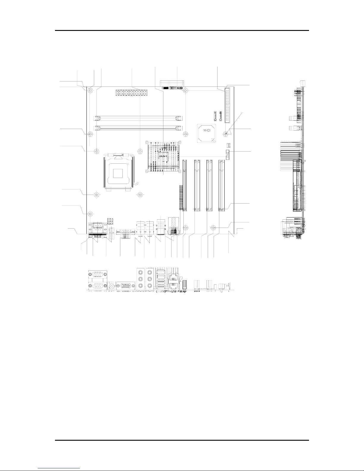
1.3.1 Mechanical Drawing
243.84
6.35
0
18.50
41.60
64.80
89.40
144.20
104.50
122.70
155.11
178.77
160.36
163.83
219.41
199.09
209.55
237.49
165.10
127.69
41.28
10.16
16.70
163.83
127.08
163.83
229.87
88.70
33.02
0
64.62
165.10
136.62
0
5.20
237.49
243.84
6.35
?4 hold/ ?8 pad
-12PCS
Page 10
System Overview
RUBY-9712VG2A User’s Manual 1-6
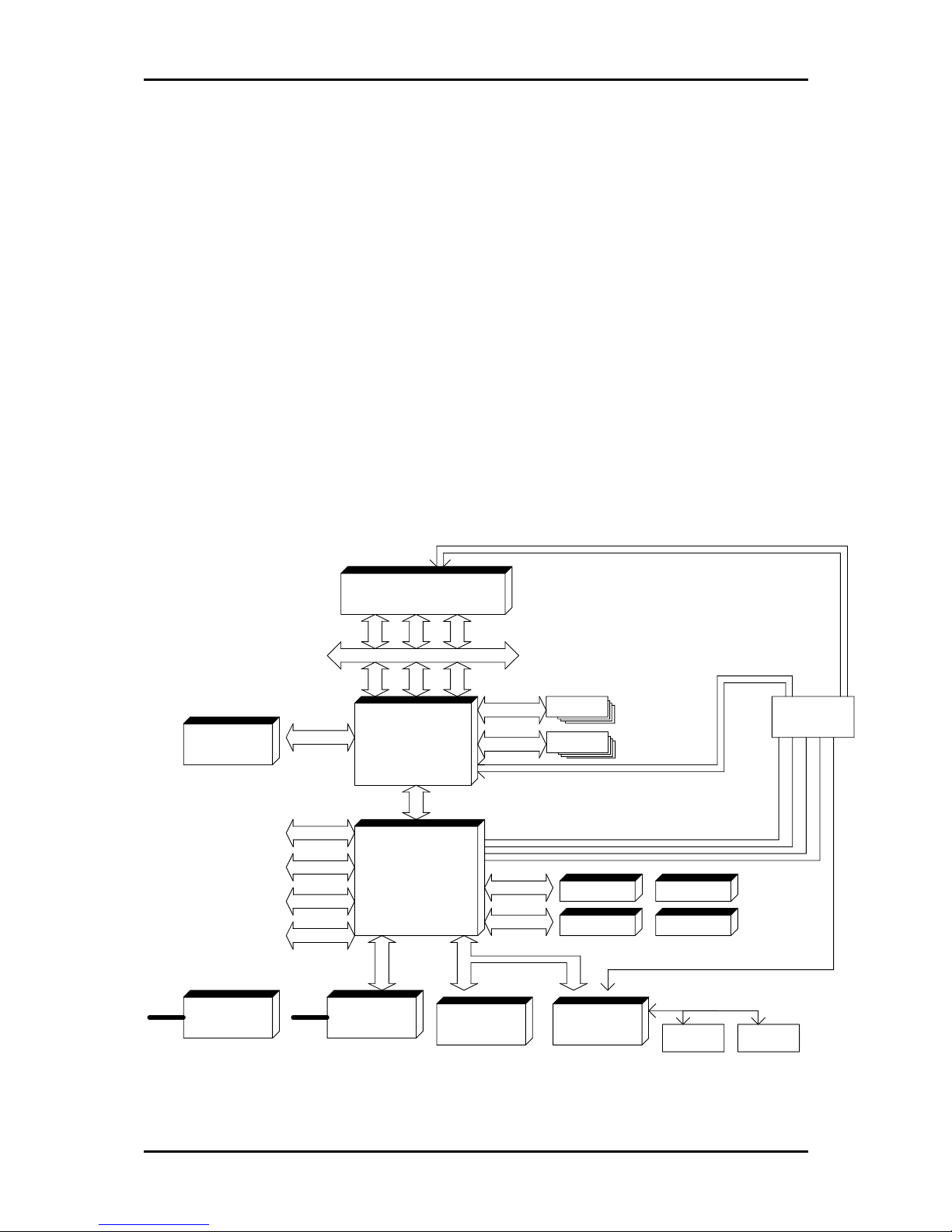
1.4 System Architecture
RUBY-9712VG2A includes Intel 915GV PCI Express chipset, Marvell 88E8053 PCI
Express x1 interface Gigabit Ethernet controller, Realtek ALC880 High Definition
Audio Codec and Winbond Super I/O.
The 915GV chipset supports the latest LGA775 package Intel Pentium 4 and Celeron
D processor with 800/533MHz front side bus; up to 2GB DDR 333/400 SDRAM
system memory in dual DIMM sockets; four PCI master; three SATA ports; one IDE
port and six USB 2.0 ports on RUBY-9712VG2A.
The Realtek ALC880 7.1 Channel High Definition Audio codecs also supports 32-bit
SPDIF input and output functions and sampling rate up to 96kHz, offering easy
connection to high quality consumer electronic products such as AC-3
decoders/speakers and mini disk devices.
Winboard Super I/O provides connection of PS/2 interface keyboard & mouse; dual
serial port; one parallel port; Watch-dog timer and GPIO interface.
C
T
R
L
33MHz
GBE
1000MB/s (10Gbps)
LPC
SATA 150M B/s
SATA #2
A
D
D
R
W83627THF
CLK410
82801F
IO
DDR DIMM B
PCI-E x1
1000Mb/s
PHY
FWH
A
D
D
R
Serial 2
PCI-E x1
33MHz
PCI-E x16
D
A
T
A
P
C
I
B
U
S
66MHz
AGTL+ BUS
PCI-E x1
DDR DIMM A
FSB800 4.3GB/s 800MT/s
FSB533 3.2GB/s 533MT/s
UDMA 33/66//100
2.5Gb/s
CH-B
L
P
C
B
U
S
133/200MHz
Video
250MB/s
1000Mb/s
PHY
1.5Gb/s
Pres cott / Tej as
HCLK
14.318MHz
Grantsdal e
MCH
BGA1209
IDE Prim ary
PCI Express core clock 250MHz
Generated from fixed 100MHz
3.2GB/s(Single/Dual,Asymmetric,D DR333/400)
8.5GB/s(Dual,Interleaved,DDR2-53 3)
D
A
T
A
CH-A
Serial 1
IDE
L G A 7 7 5
C
T
R
L
I C H 6
BGA609
48MHz
GBE
FSB 800/533 Mhz
PCI-E x1
CF CARD
S y s t e m B l o c k D i a g r a m
Direct Media Interface
DMI 4 Lanes
L040
SATA #1
P r o c e s s o r
BCLK0
RUBY-9712VG2A Block Diagram
Page 11
Hardware Configuration
RUBY-9712VG2A User’s Manual 2-1
Chapter 2
Hardware Configuration
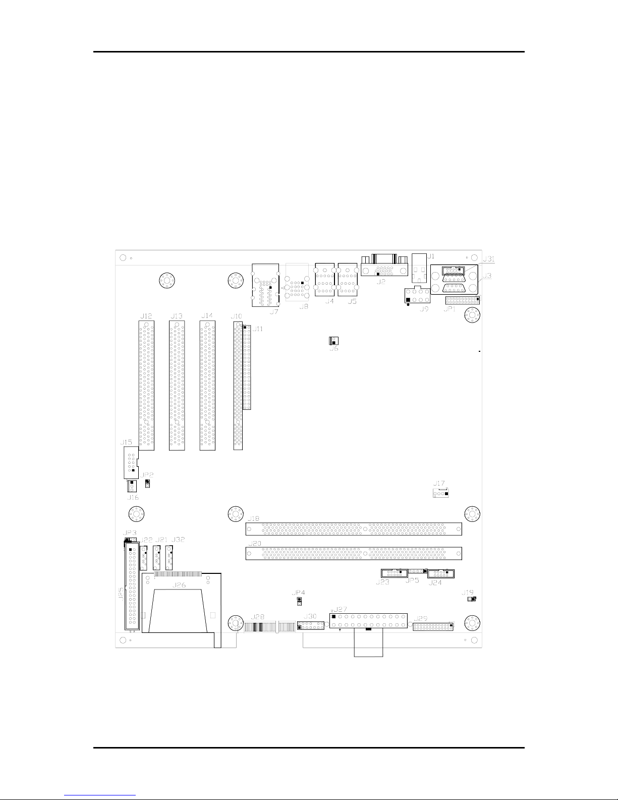
This chapter gives the definitions and shows the positions of jumpers, headers and
connector. All of the configuration jumpers on RUBY-9712VG2A are in the proper
position. The default settings shipped from factory are marked with a star (Ì).
2.1 Jumper Setting
Figure 2-1 RUBY-9712VG2A Jumper & Connector Location
Page 12
Hardware Configuration
RUBY-9712VG2A User’s Manual 2-2
1 2
21 19 17 15 13 11 9 7 5 3 1
22 20 18 16 14 12 10
8 6 4 2
21 19 17 15 13 11 9 7 5 3 1
22 20 18 16 14 12 10 8 6 4 2
21 19 17 15 13 11 9 7 5 3 1
22 20 18 16 14 12 10 8 6 4 2
21 19 17 15 13 11 9 7 5 3 1
21 19 17 15 13 11 9 7 5 3 1
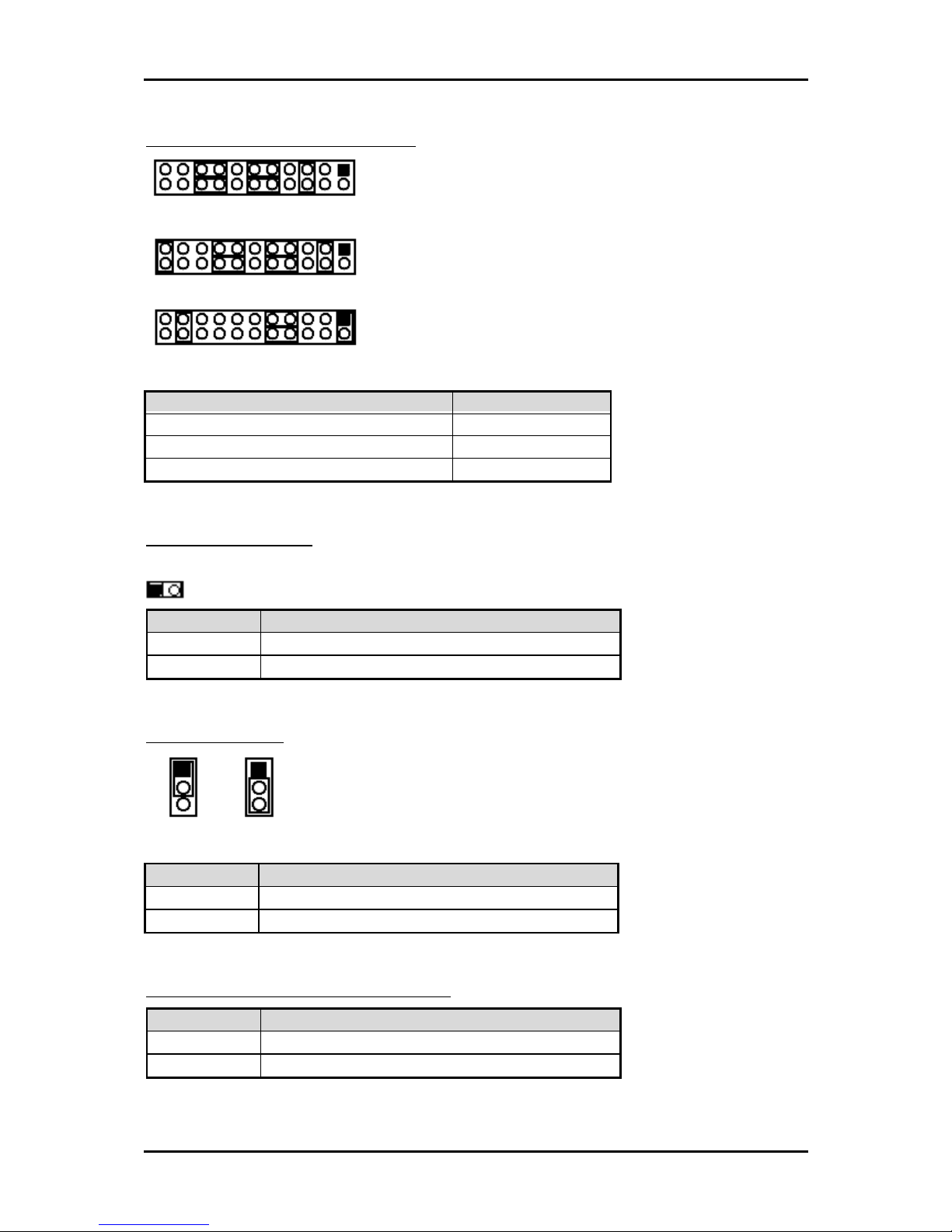
JP1: COM1(J3) Interface Selection
J
P1
5-6,9-11,10-12,15-17,16-18 Short RS-232 Ì
3-4,7-9,8-10,13-15,14-16,21-22 Short RS-422
1-2,7-9,8-10,19-20 Short RS-485
JP2: Factory test only
JP2 Function
Open Normal Ì
Short Factory Test
JP3: CMOS Clear
Normal Clear
JP3 Function
1-2 Short Clear CMOS Disable (Normal) Ì
2-3 Short Clear CMOS Enable (Clear)
JP4: Watch Dog Timer Enable/Disable
JP4 Function
Short Watch Dog Enable (Normal) Ì
Open Watch Dog Disable
RS-232
RS-422
RS-485
1
2
3
1
2
3
Page 13
Hardware Configuration
RUBY-9712VG2A User’s Manual 2-3
5 4 3 2 1
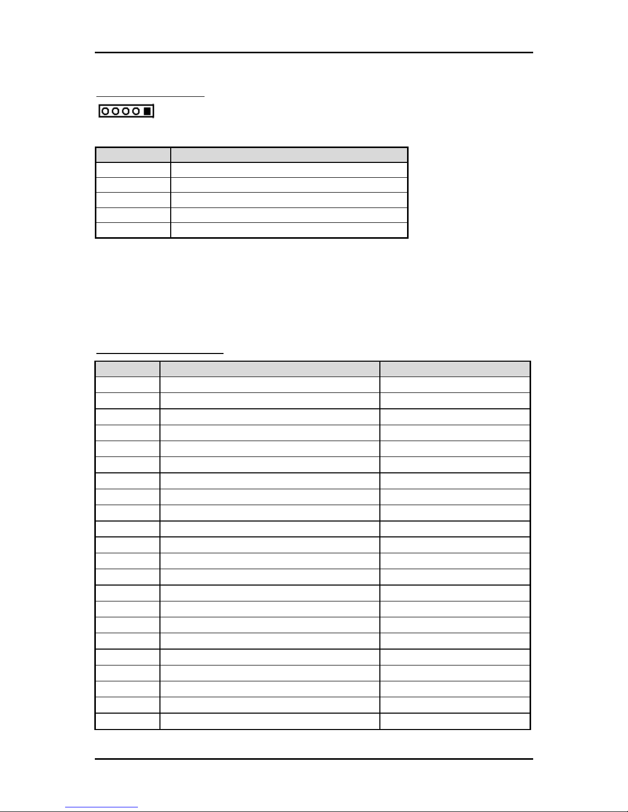
JP5: IrDA Connector
PIN No. Signal Description
1 +5V
2 IRRX
3 IRTX
4 NC
5 Ground
2.2 Connector Allocation
I/O peripheral devices are connected to the interface connectors on this Embedded
ATX computer.
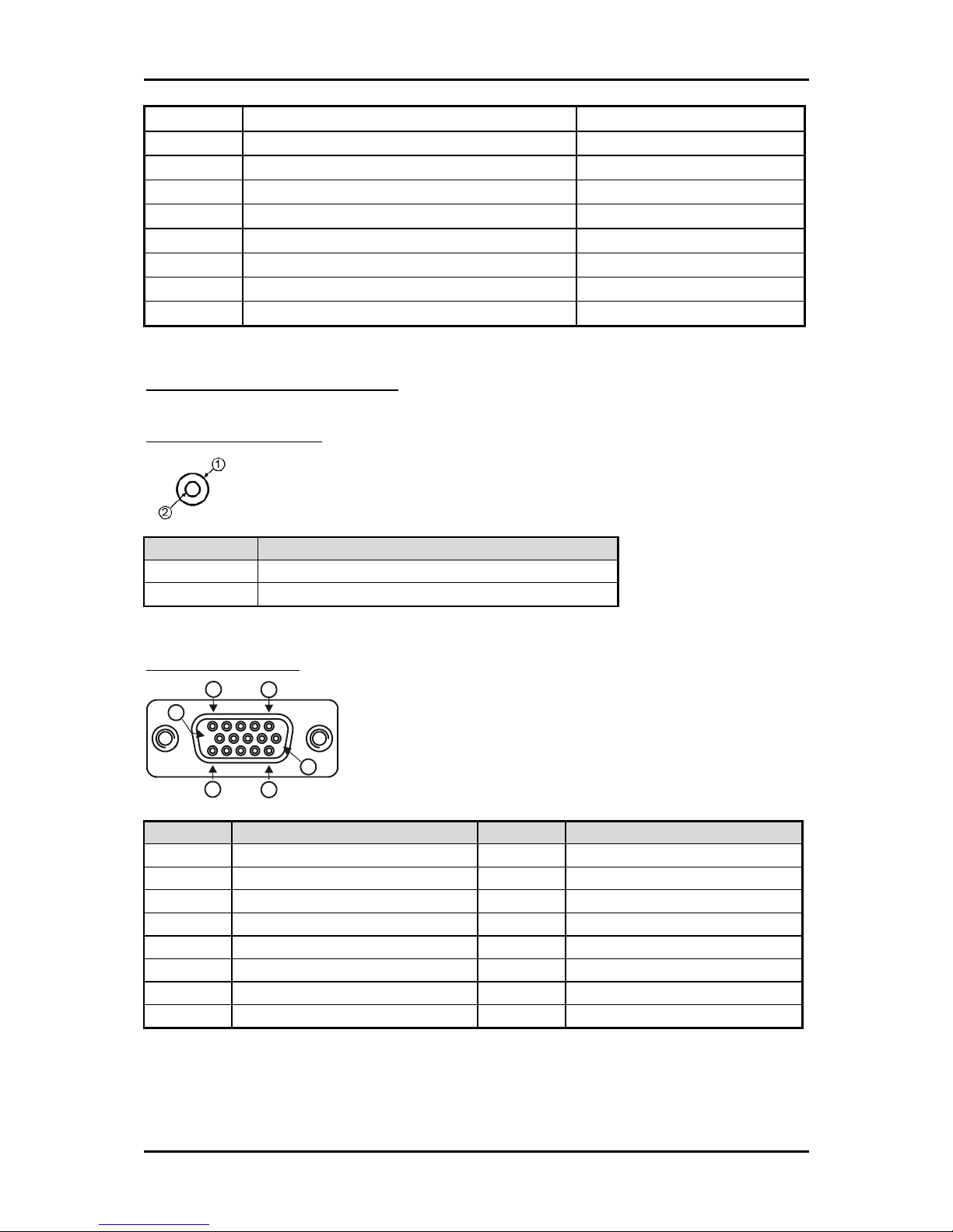
Connector Function List
Connector Description Remark
J1 SPDIF out port
J2 VGA out port
J3 COM1/COM2 port
J4 Audio ports
J5 Audio surround ports
J6 SPDIF in port
J7 LAN port 1/2
J8 USB port 1/2/3/4
J9 ATX 12V power connector
J10 PCI slot 4
J11 SDVO port
J12 PCI slot 1
J13 PCI slot 2
J14 PCI slot 3 and Riser card
J15 USB port 5/6
J16 System FAN connector
J17 CPU FAN connector
J18 DDR channel A
J19 Case Open
J20 DDR channel B
J21 SATA port 2
J22 SATA port 1
Page 14
Hardware Configuration
RUBY-9712VG2A User’s Manual 2-4
J23 GPIO
J24 PS/2 Keyboard and Mouse
J25 IDE connector
J26 CF card
J27 Main ATX power connector
J28 4 PCI Express x1 ports
J29 Printer port
J30 Front panel connector
J32 SATA port 3
Pin Assignments of Connectors
J1: SPDIF OUT PORT
PIN No. Signal Description
1 Ground
2 SPDIF OUT PORT
J2: VGA Connector
1
11
15
5
10
6
PIN No. Signal Description PIN No. Signal Description
1 RED 2 GREEN
3 BLUE 4 ID0
5 Ground 6 Ground
7 Ground 8 Ground
9 NC 10 Ground
11 ID1 12 DDCDATA
13 HSYNC 14 VSYNC
15 DDCCLK
Page 15
Hardware Configuration
RUBY-9712VG2A User’s Manual 2-5
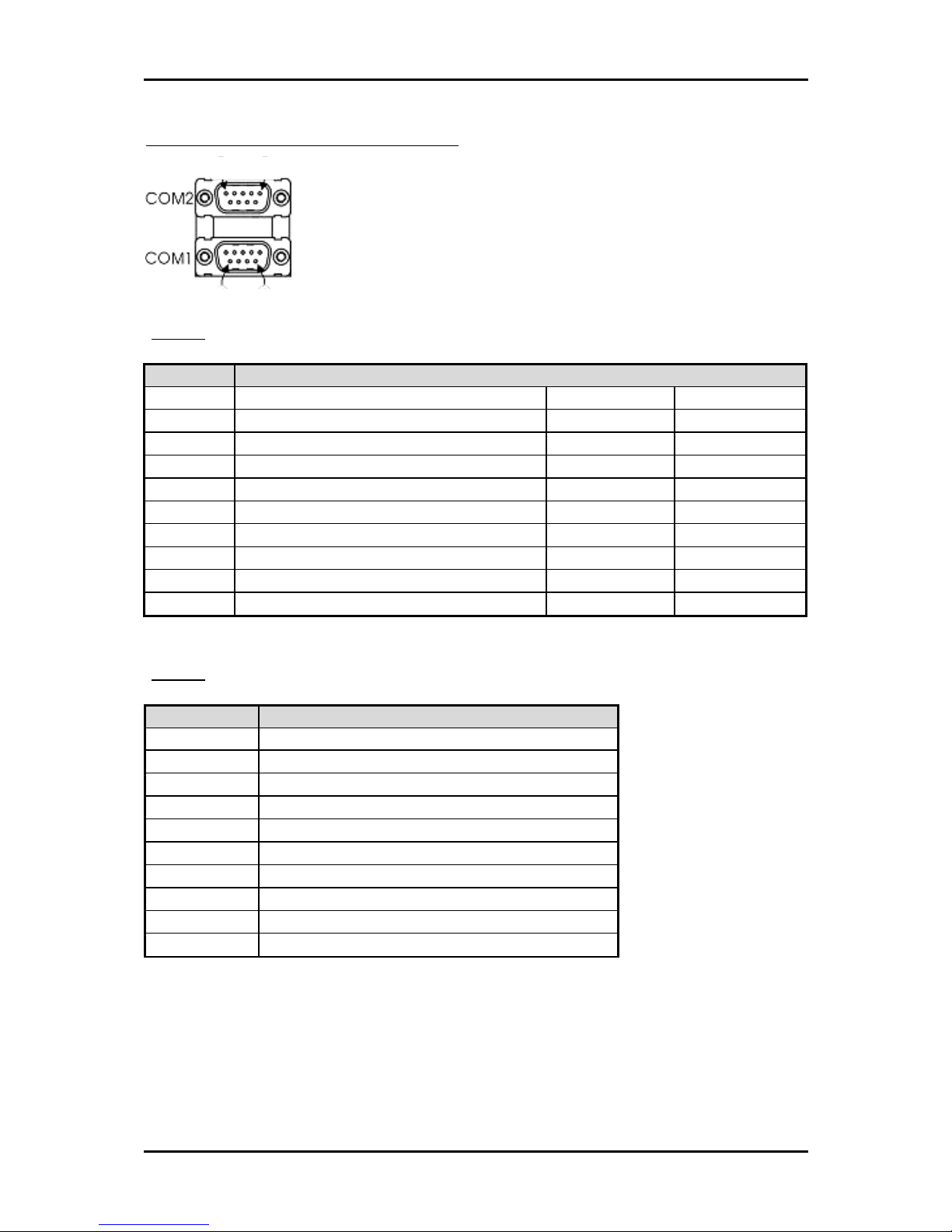
J3: COM1/COM2 Serial Port Connector
-COM1
PIN No. Signal Description
RS-232 RS-422 RS-485
1 DCD (Data Carrier Detect) TX- DATA2 RXD (Receive Data) TX+ DATA+
3 TXD (Transmit Data) RX+ NC
4 DTR (Data Terminal Ready) RX- NC
5 GND (Ground) GND GND
6 DSR (Data Set Ready) NC NC
7 RTS (Request to Send) NC NC
8 CTS (Clear to Send) NC NC
9 RI (Ring Indicator) NC NC
-COM2
PIN No. Signal Description
RS-232
1 DCD (Data Carrier Detect)
2 RXD (Receive Data)
3 TXD (Transmit Data)
4 DTR (Data Terminal Ready)
5 GND (Ground)
6 DSR (Data Set Ready)
7 RTS (Request to Send)
8 CTS (Clear to Send)
9 RI (Ring Indicator) or +12V
1 5
6 9
Page 16
Hardware Configuration
RUBY-9712VG2A User’s Manual 2-6
2 1
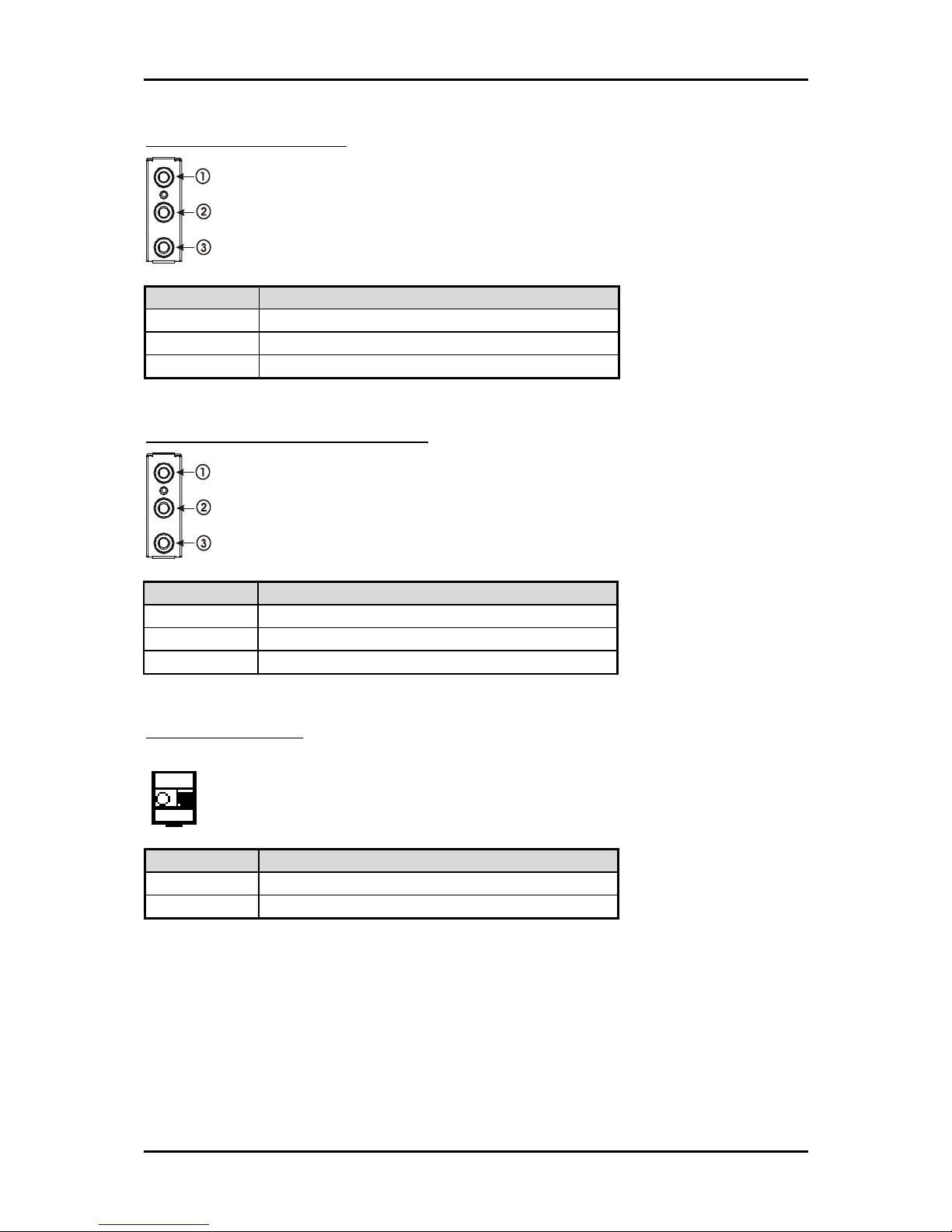
J4: Audio Jack Connector
PIN No. Signal Description
1 (Blue) Line In
2 (Lime) Line Out / Front Right, Left Channel
3 (Pink) Mic In
J5: Audio Surround Jack Connector
PIN No. Signal Description
1 (Orange) Surround Side Left / Right Channel
2 (Black) Surround Rear Left / Right Channel
3 (Gray) Center / LFE Channel
J6: SPDIF IN PORT
PIN No. Signal Description
1 Ground
2 SPDIF IN PORT
Page 17
Hardware Configuration
RUBY-9712VG2A User’s Manual 2-7
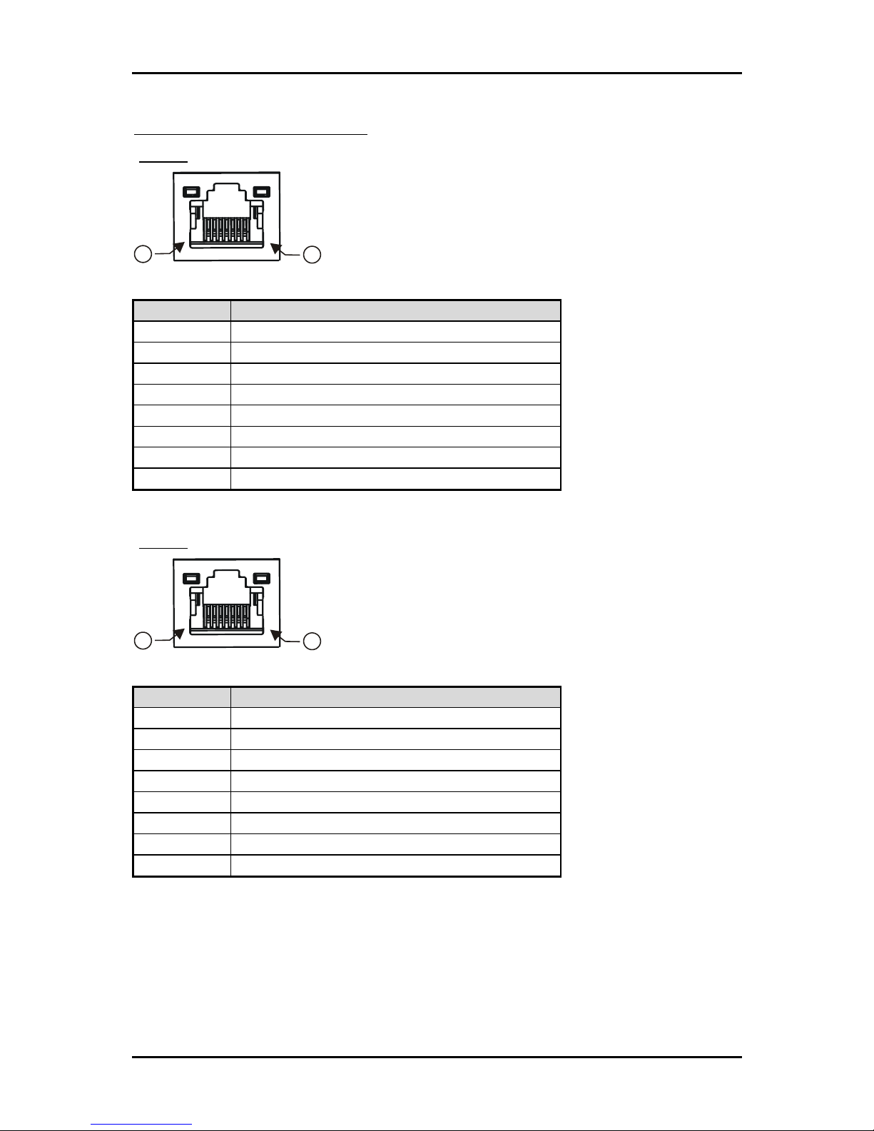
J7: Ethernet 1/2 RJ-45 Connector
-LAN 1
1
8
PIN No. Signal Description
1 TD+ (MDI0+)
2 TD- (MDI0-)
3 RD+ (MDI1+)
4 MDI2+
5 MDI26 RD- (MDI1-)
7 RD+
8 RD-
-LAN 2
1
8
PIN No. Signal Description
1 TD+ (MDI0+)
2 TD- (MDI0-)
3 RD+ (MDI1+)
4 MDI2+
5 MDI26 RD- (MDI1-)
7 MDI3+
8 MDI3-
Page 18
Hardware Configuration
RUBY-9712VG2A User’s Manual 2-8
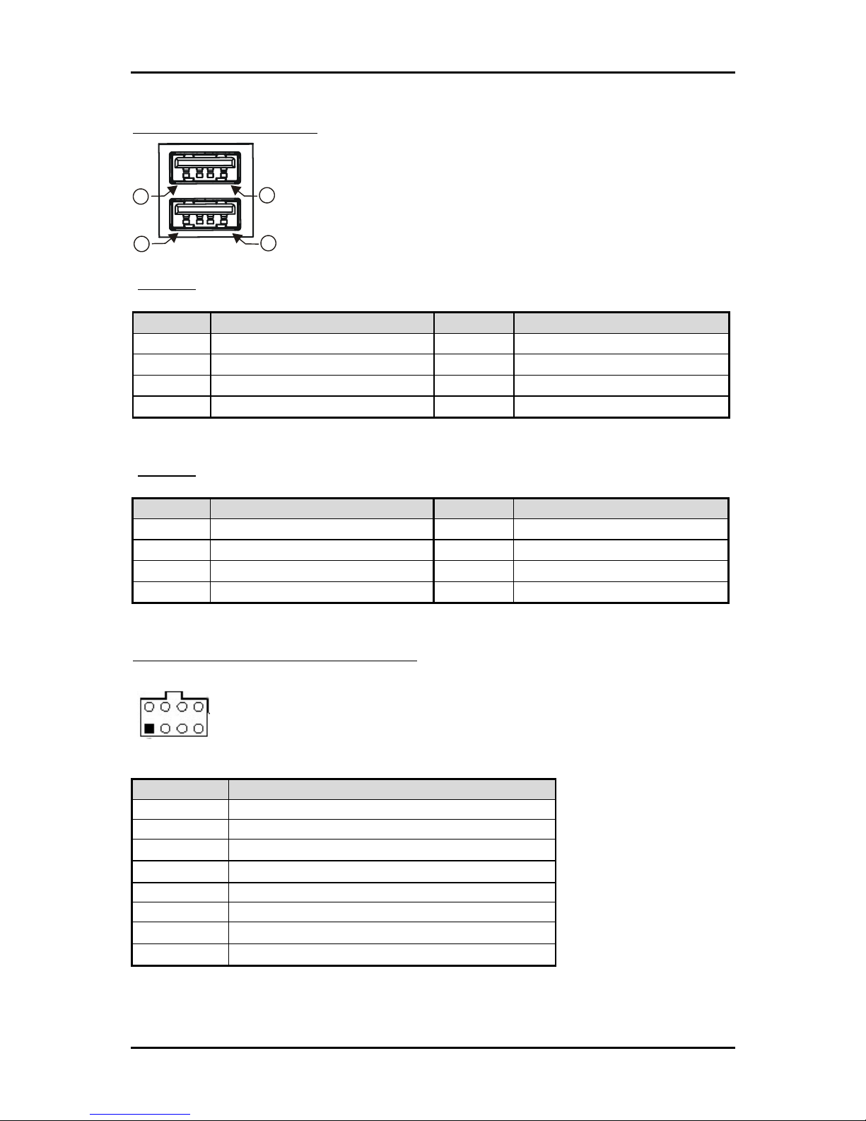
J8: USB 1/2/3/4 Connector
1
4
5
8
-USB 1/2
PIN No. Signal Description PIN No. Signal Description
1 +5VSB 5 +5VSB
2 Data - 6 Data 3 Data + 7 Data +
4 GND 8 GND
-USB 3/4
PIN No. Signal Description PIN No. Signal Description
1 +5V 5 +5V
2 Data - 6 Data 3 Data + 7 Data +
4 GND 8 GND
J9: 12V CPU Supplementary Connector
PIN No. Signal Description
1 Ground
2 Ground
3
Ground ※
4
Ground ※
5 +12V
6 +12V
7
+12V ※
8
+12V ※
Note:
※ When using 4-pin 12V CPU supplementary connector, plug the power connector into pins as marked.
5 6 7 8
1 2 3 4
Page 19
Hardware Configuration
RUBY-9712VG2A User’s Manual 2-9
44 43 42 41 40 39 38 37 36 35 34 33 32 31 30 29 28 27 26 25 24 23
6 7 8 9 10
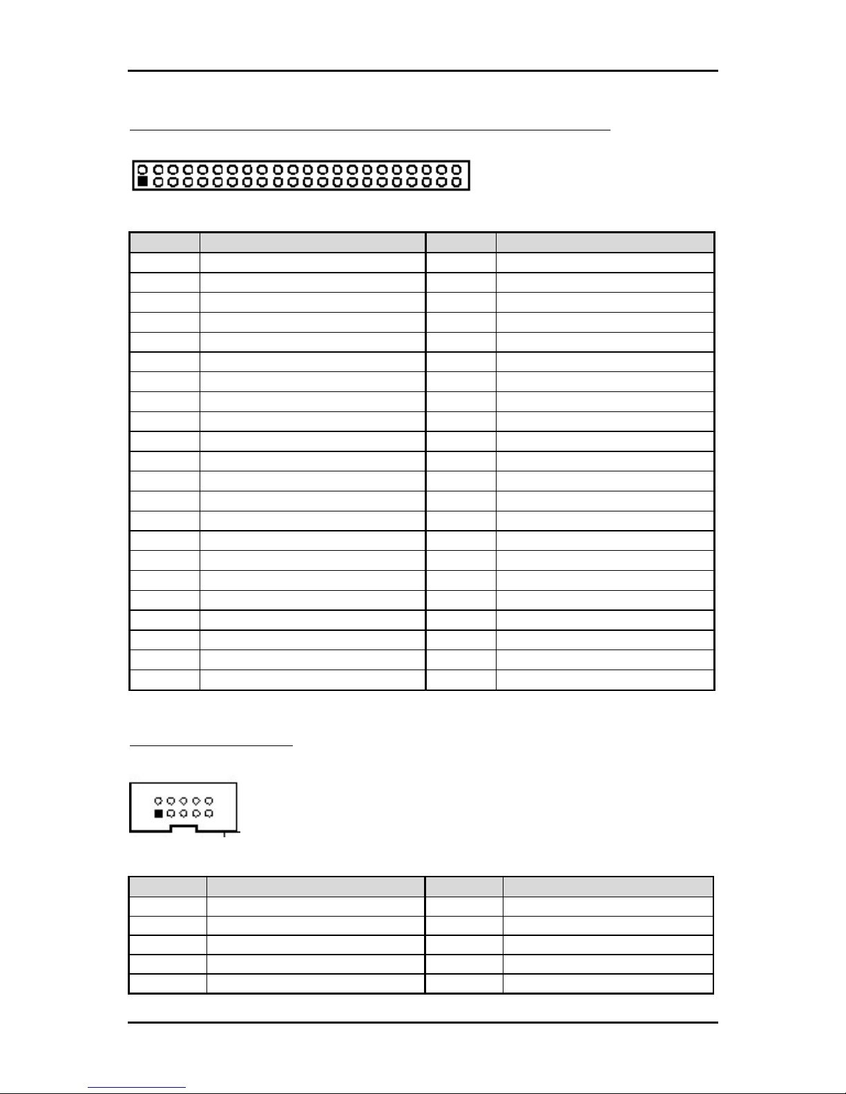
J11: SDVO Connector (Factory Optional for Panel Display Kit only)
PIN No. Signal Description PIN No. Signal Description
1 +12V 23 +12V
2 +12V 24 SDVO TVCLK3 SDVO B Blue+ 25 SDVO TVCLK+
4 SDVO B Blue- 26 Ground
5 Ground 27 SDVO B Red6 SDVO B CLOCK+ 28 SDVO B Red+
7 SDVO B CLOCK- 29 Ground
8 Ground 30 SDVO B Green-
9 SDVO Control DATA 31 SDVO B Green+
10 SDVO Control CLK 32 Ground
11 Ground 33 SDVO C INT+
12 SDVO C Red- 34 SDVO C INT13 SDVO C Red+ 35 Ground
14 Ground 36 SDVO Stall15 SDVO C Green+ 37 SDVO Stall+
16 SDVO C Green- 38 Ground
17 Ground 39 SDVO B INT18 SDVO C Blue+ 40 SDVO B INT+
19 SDVO C Blue- 41 Ground
20 VCC3 42 SDVO C CLOCK21 VCC3 43 SDVO C CLOCK+
22 CHIPRST- 44 Ground
J15: USB 5/6 Connector
PIN No. Signal Description PIN No. Signal Description
1 NC 6 +5V
2 Ground 7 Data 3 Data + 8 Data +
4 Data - 9 Ground
5 +5V 10 NC
Page 20
Hardware Configuration
RUBY-9712VG2A User’s Manual 2-10
1 2 3 4
2 1
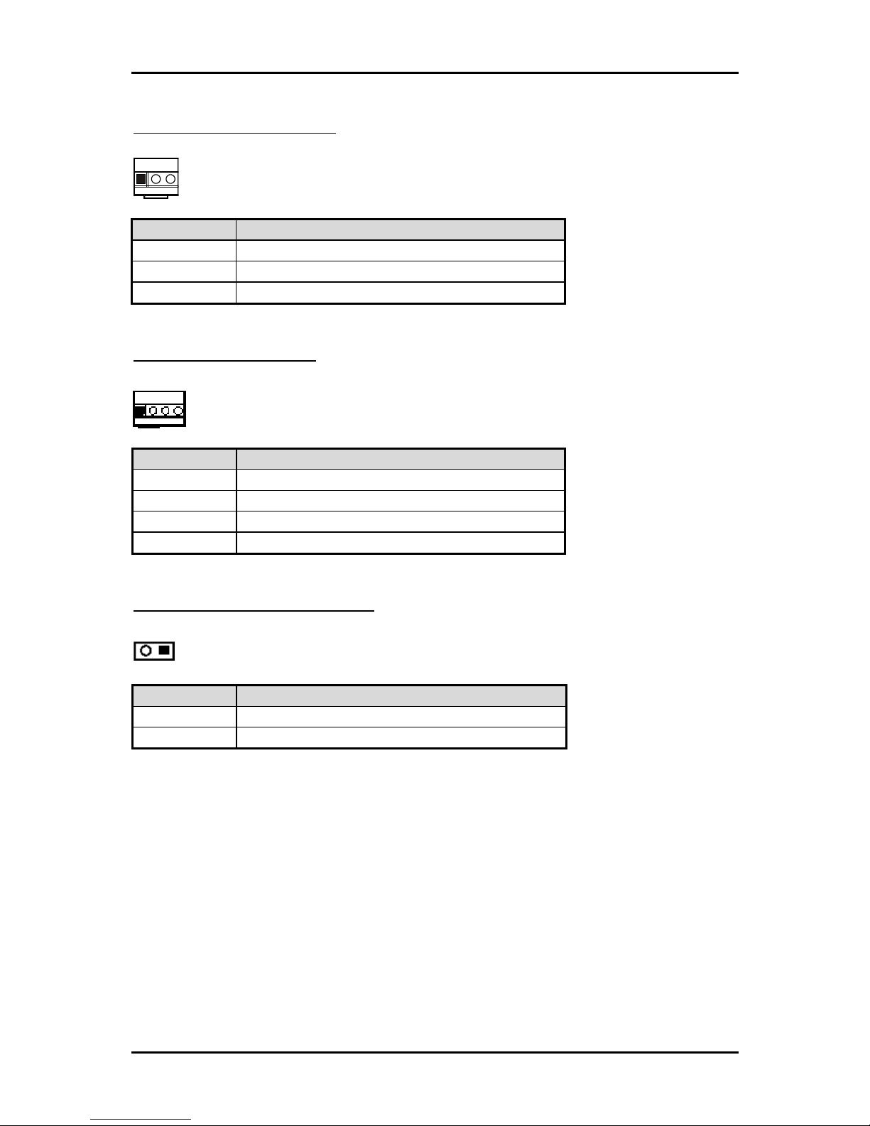
J16: System FAN Connector
123
PIN No. Signal Description
1 Ground
2 +12V
3 Fan Speed Detecting signal
J17: CPU FAN Connector
PIN No. Signal Description
1 Ground
2 +12V
3 Sense (Fan Speed Detecting signal)
4 Control (PWM)
J19: Case Open Detect Connector
PIN No. Signal Description
1 Case Open; Short: case open
2 Ground
Page 21
Hardware Configuration
RUBY-9712VG2A User’s Manual 2-11
1 2 3 4 5
2 3 5 6
1 4 7
J21/J22/J32: SATA Connector
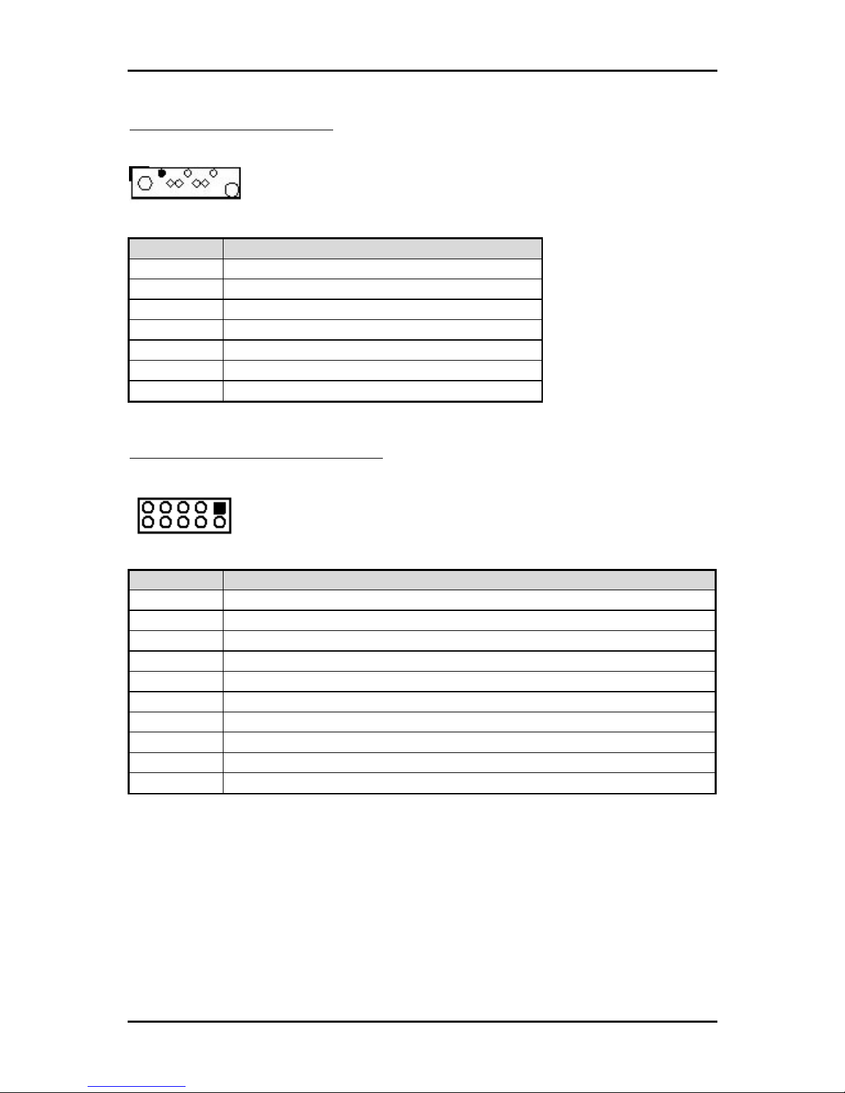
PIN No. Signal Description
1 Ground
2 TX+
3 TX4 Ground
5 RX6 RX+
7 Ground
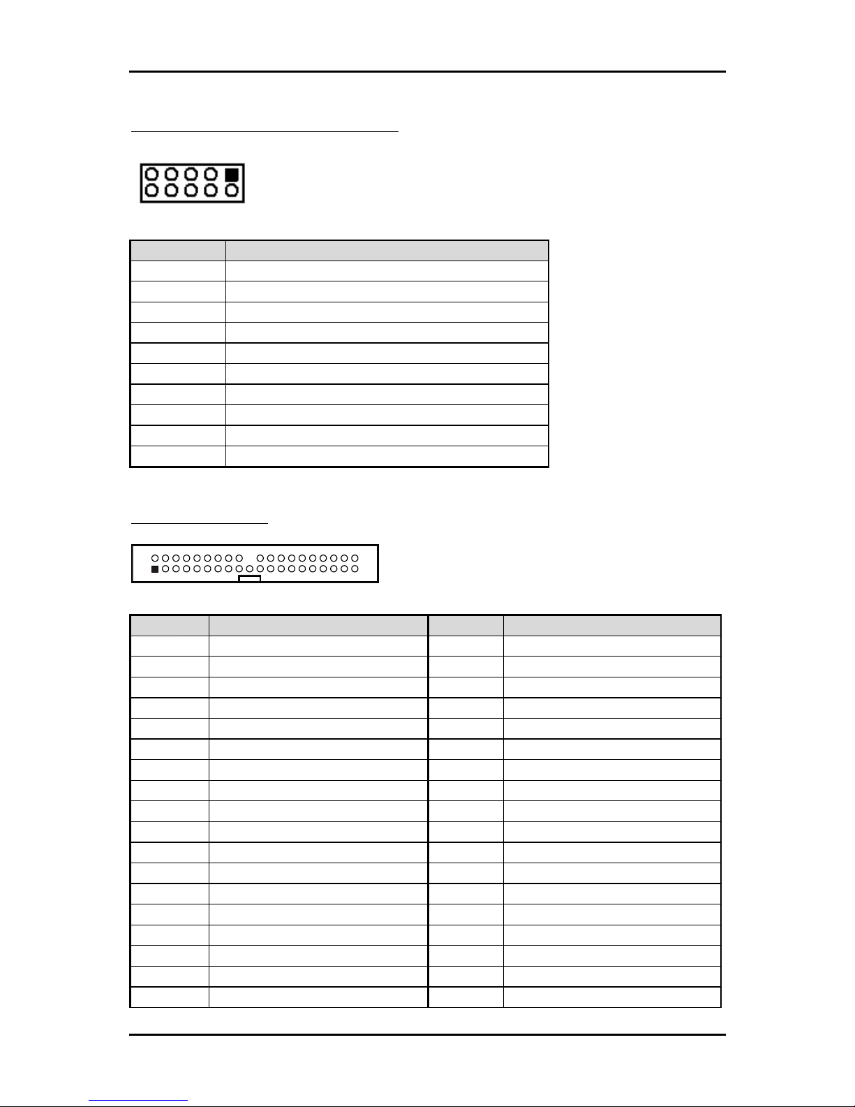
J23: General Purpose I/O Connector
PIN No. Signal Description
1 General Purpose I/O Port 1 (GPIO1) SIO-GP26
2 General Purpose I/O Port 2 (GPIO2) SIO-GP25
3 General Purpose I/O Port 3 (GPIO3) SIO-GP24
4 General Purpose I/O Port 4 (GPIO4) SIO-GP23
5 Ground
6 Buffered Digital Output Port 1 (DO1) SIO-GP10
7 Buffered Digital Output Port 2 (DO2) SIO-GP11
8 Buffered Digital Output Port 3 (DO3) SIO-GP12
9 Buffered Digital Output Port 4 (DO4) SIO-GP13
10 +5V
Page 22
Hardware Configuration
RUBY-9712VG2A User’s Manual 2-12
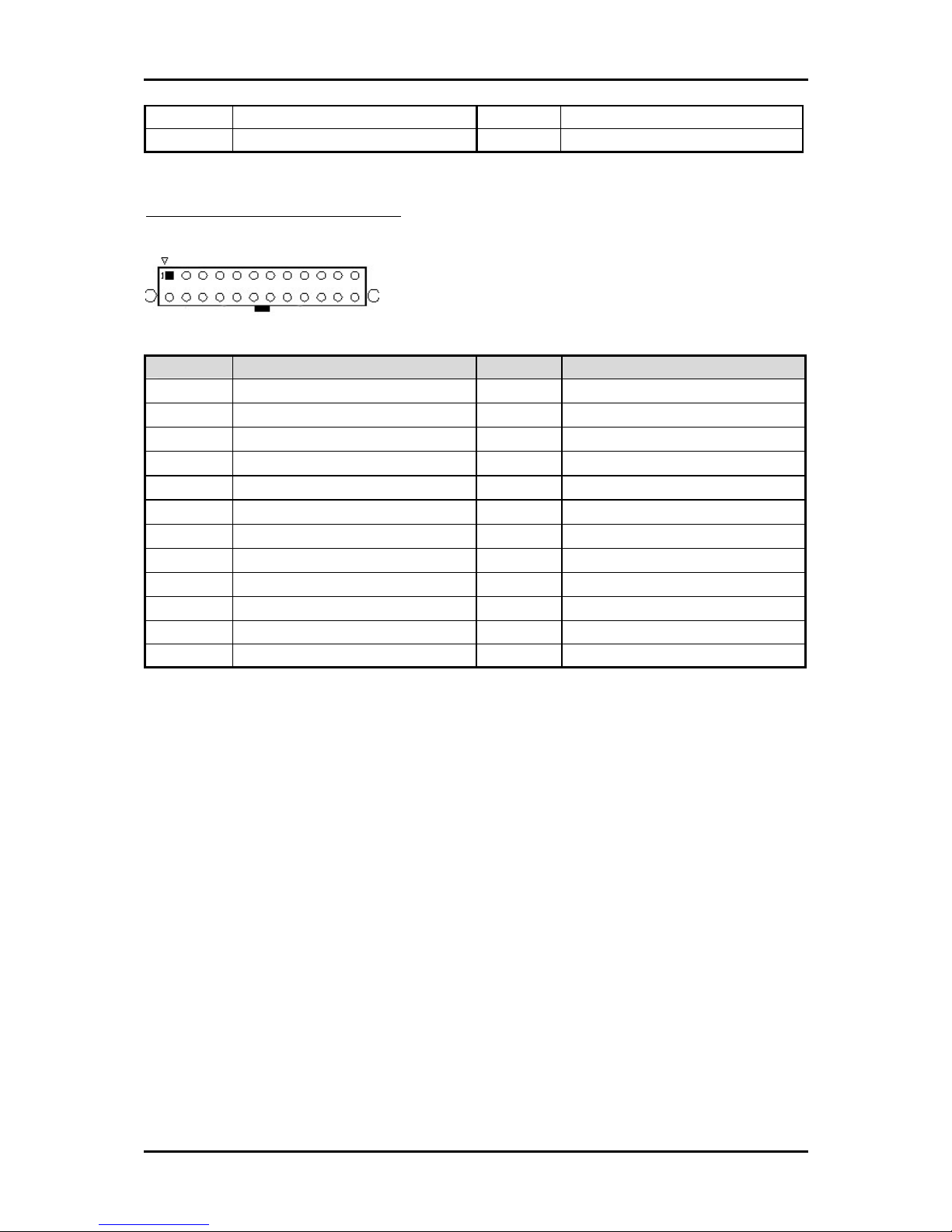
J24: PS/2 Keyboard Mouse Connector
PIN No. Signal Description
1 Mouse Data
2 NC
3 Ground
4 +5VSB
5 Mouse Clock
6 Keyboard Data
7 NC
8 Ground
9 +5VSB
10 Keyboard Clock
J25: IDE Connector
1
2
39
40
PIN No. Signal Description PIN No. Signal Description
1 RESET# 2 Ground
3 Data 7 4 Data 8
5 Data 6 6 Data 9
7 Data 5 8 Data 10
9 Data 4 10 Data 11
11 Data 3 12 Data 12
13 Data 2 14 Data 13
15 Data 1 16 Data 14
17 Data 0 18 Data 15
19 Ground 20 NC
21 DMA REQ 22 Ground
23 IOW# 24 Ground
25 IOR# 26 Ground
27 IOCHRDY 28 Pull-down
29 DMA ACK# 30 Ground
31 INT REQ 32 NC
33 SA1 34 CBLID#
35 SA0 36 SA2
Page 23
Hardware Configuration
RUBY-9712VG2A User’s Manual 2-13
13 14
37 HDC CS0# 38 HDC CS1#
39 HDD Active# 40 Ground
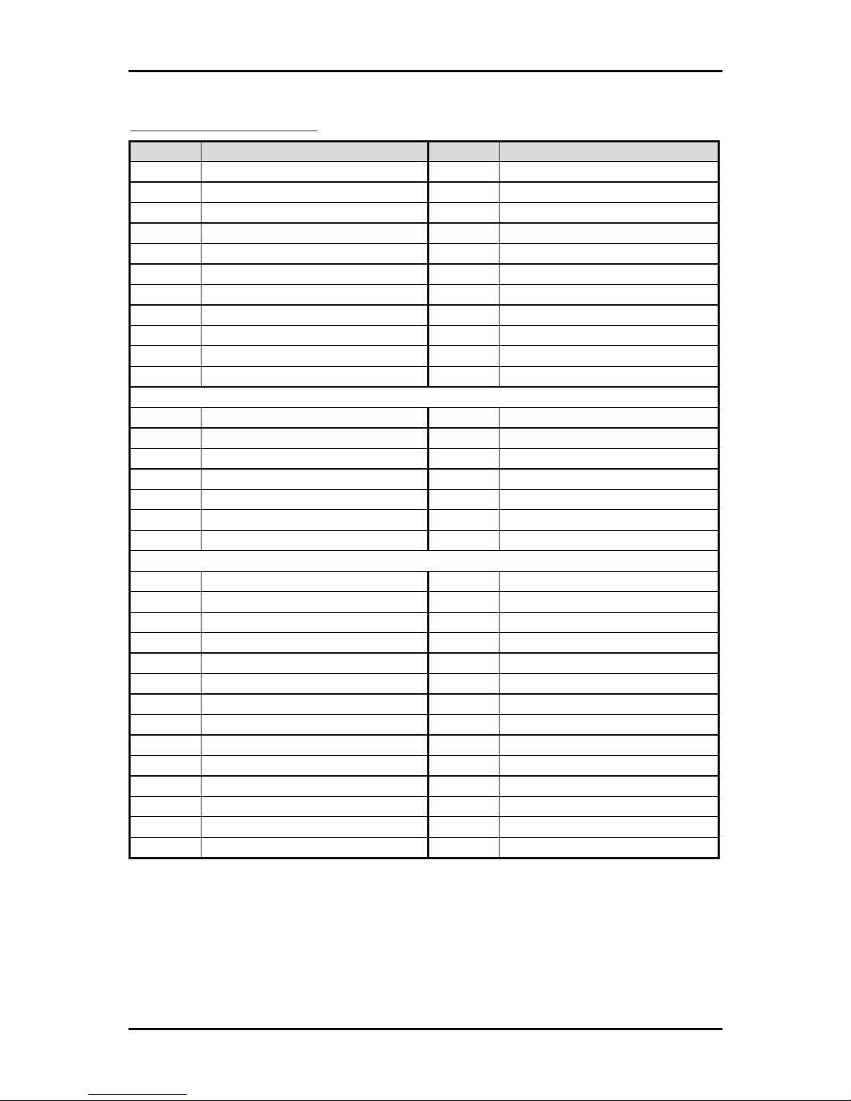
J27: Main ATX power connector
PIN No. Signal Description PIN No. Signal Description
1 +3.3VDC ※ 13 +3.3VDC ※
2 +3.3VDC ※ 14 -12VDC ※
3 COM ※ 15 COM ※
4 +5VDC ※ 16 PS_ON# ※
5 COM ※ 17 COM ※
6 +5VDC ※ 18 COM ※
7 COM ※ 19 COM ※
8 PWR_OK ※ 20 -5VDC ※
9 +5VSB ※ 21 +5VDC ※
10 +12VDC ※ 22 +5VDC ※
11 +12VDC 23 +5VDC
12 +3.3VDC 24 COM
Note:
※ When using 20-pin ATX power connector, plug the power connector into pins as
marked.
Page 24
Hardware Configuration
RUBY-9712VG2A User’s Manual 2-14
J28: 4 PCI Express x1 ports
PIN No. Signal Description PIN No. Signal Description
B1 +12V A1 PRSNT1B2 +12V A2 +12V
B3 +12V A3 +12V
B4 Ground A4 Ground
B5 PCLKp1 A5 PCLKp2
B6 PCLKn1 A6 PCLKn2
B7 Ground A7 TDO
B8 +3.3V A8 TMS
B9 JTAG A9 +3.3V
B10 +3.3VAUX A10 +3.3V
B11 WAKE- A11 RESET-
Mechanical KEY
B12 Reserved A12 Ground
B13 Ground A13 PCLKp0
B14 PETp1 A14 PCLKn0
B15 PETn1 A15 Ground
B16 Ground A16 PERp0
B17 PRSNT2- A17 PERn0
B18 Ground A18 Ground
End of the x1 connector
B19 PETp1 A19 Reserved
B20 PETn1 A20 Ground
B21 Ground A21 PERp1
B22 Ground A22 PERn1
B23 PETp2 A23 Ground
B24 PETn2 A24 Ground
B25 Ground A25 PERp2
B26 Ground A26 PERn2
B27 PETp3 A27 Ground
B28 PETn3 A28 Ground
B29 Ground A29 PERp3
B30 PCLKp3 A30 PERn3
B31 PCLKn3 A31 Ground
B32 Ground A31 +3.3V
Page 25
Hardware Configuration
RUBY-9712VG2A User’s Manual 2-15
13 12 11 10 9 8 7 6 5 4 3 2 1
25 24 23 22 21 20 19 18 17 16 15 14
J29: Parallel Port Connector
PIN No. Signal Description PIN No. Signal Description
1 Strobe# 14 Auto Form Feed#
2 Data 0 15 Error#
3 Data 1 16 Initialization#
4 Data 2 17 Printer Select IN#
5 Data 3 18 Ground
6 Data 4 19 Ground
7 Data 5 20 Ground
8 Data 6 21 Ground
9 Data 7 22 Ground
10 Acknowledge# 23 Ground
11 Busy 24 Ground
12 Paper Empty 25 Ground
13 Printer Select 26 NC
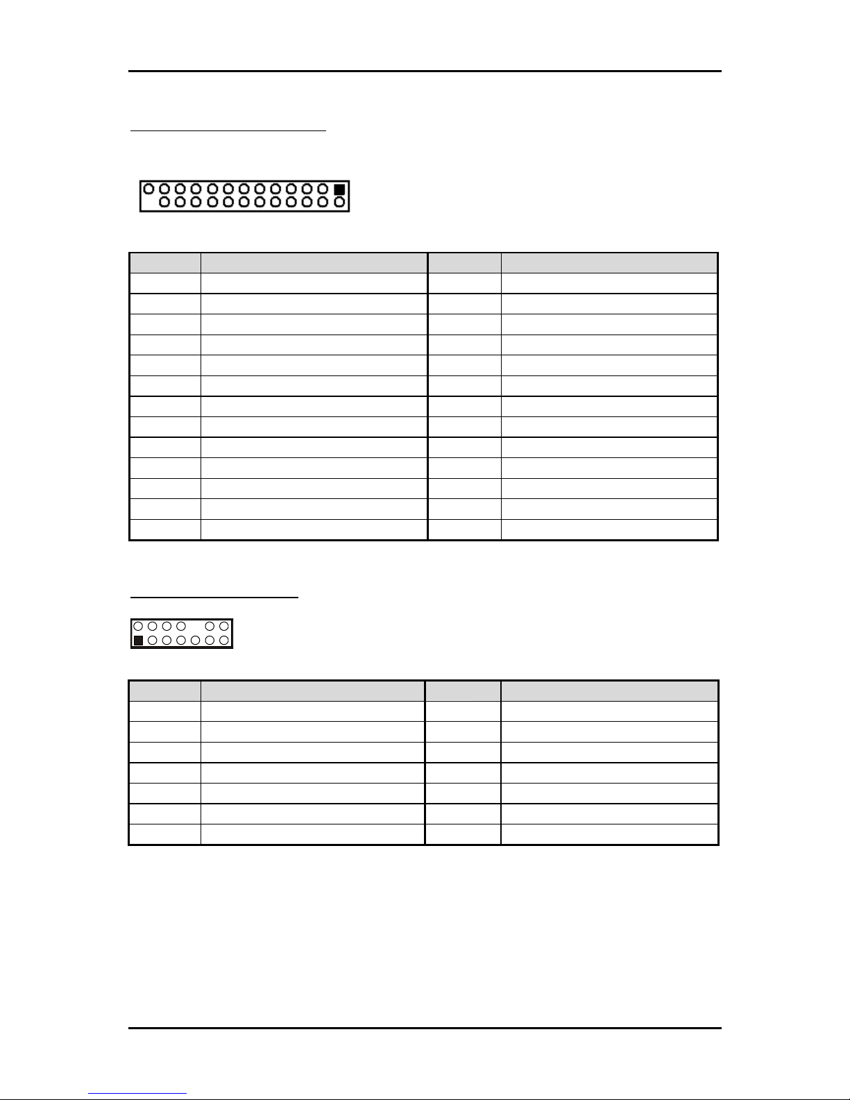
J30: Power/LED Header
1
2
14
1
3
PIN No. Signal Description PIN No. Signal Description
1 HDD_LED+5V (330 ohm) 2 POWER_LED+5V (330 ohm)
3 HDD_LED- 4 POWER_LED-
5 Ground 6 Power Switch
7 Reset Switch 8 Ground
9 SERR# 10 NC
11 +5V (330 ohm) 12 +5V (330 ohm)
13 LAN_ACTLED# 14 LAN_LINKLED#
Page 26
System Installation
RUBY-9712VG2A User’s Manual 3-1
Chapter 3
System Installation
This chapter provides you with instructions to set up your system. The additional
information is enclosed to help you set up onboard PCI device and handle WDT
operation in software programming.
3.1 Pentium 4 Processor
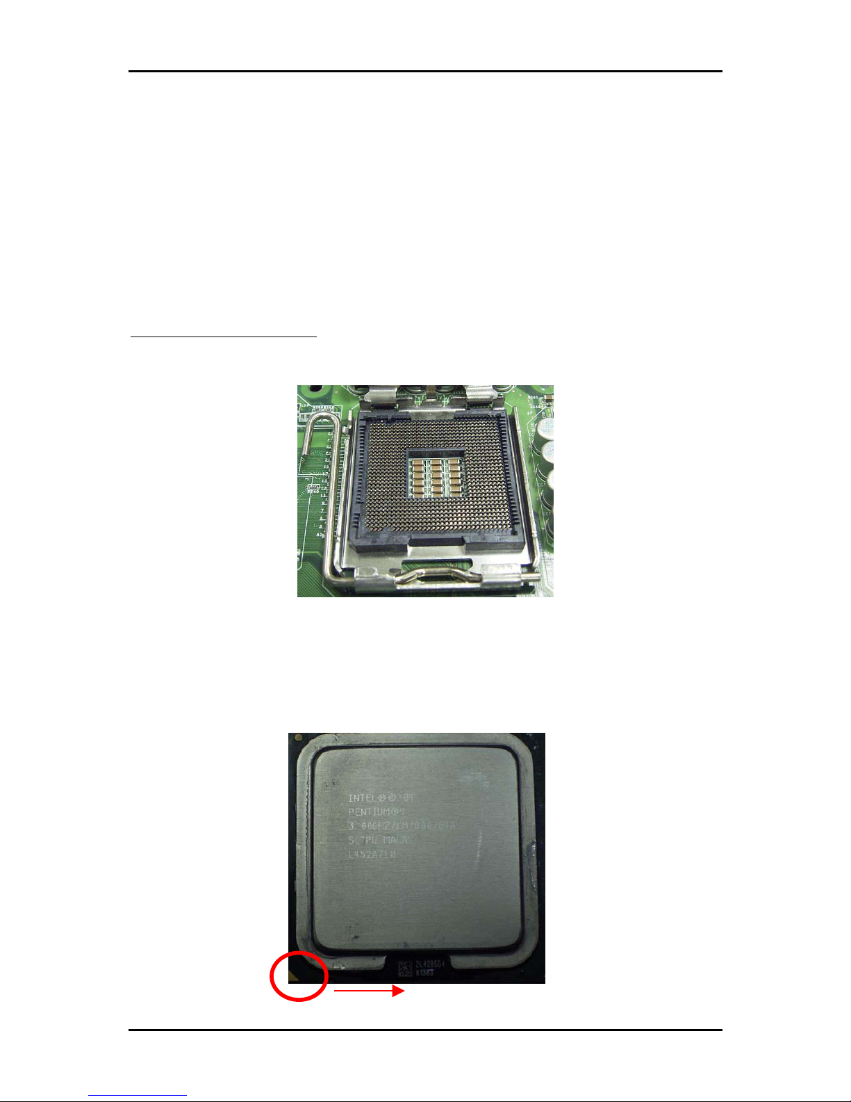
Installing Socket 775 CPU
1) Lift the handling lever of CPU socket outwards and upwards to the other end.
2) Align the processor pins with pinholes on the socket. Make sure that the notched
corner or dot mark (pin 1) of the CPU corresponds to the socket’s bevel end. Then
press the CPU gently until it fits into place. If this operation is not easy or smooth,
don’t do it forcibly. You need to check and rebuild the CPU pin uniformly.
PIN 1
Page 27
System Installation
RUBY-9712VG2A User’s Manual 3-2
3) Push down the lever to lock processor chip into the socket once CPU fits.
4) Follow the installation guide of cooling fan or heat sink to mount it on CPU
surface and lock it on the LGA 775 package.
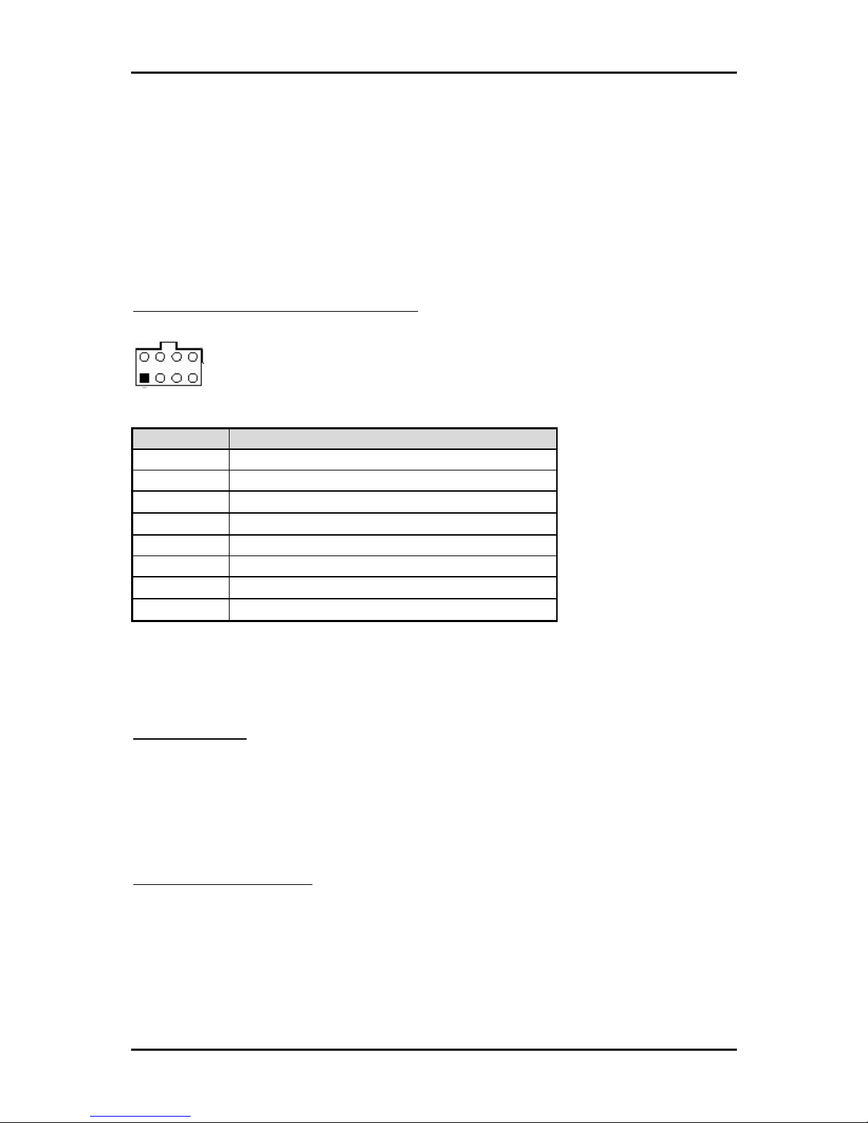
5) You should know LGA 775 processor need extra 12V power source.
Don’t forget to connect 8pin 12V connector to J9!
J9: 12V CPU Supplementary Connector
PIN No. Signal Description
1 Ground
2 Ground
3 Ground ※
4 Ground ※
5 +12V
6 +12V
7 +12V ※
8 +12V ※
Note:
※ When using 4-pin 12V CPU supplementary connector, plug the power connector
into pins as marked.
Removing CPU
1) Unlock the cooling fan first.
2) Lift the lever of CPU socket outwards and upwards to the other end.
3) Carefully lifts up the existing CPU to remove it from the socket.
4) Follow the steps of installing a CPU to change to another one or place handling
bar to close the opened socket.
Configuring System Bus
RUBY-9712VG2A will automatically detect the CPU used. CPU speed of LGA 775
can be detected automatically.
5 6 7 8
1 2 3 4
Page 28
System Installation
RUBY-9712VG2A User’s Manual 3-3
3.2 Main Memory
RUBY-9712VG2A provides two DDR-SDRAM DIMM sockets to support DDRSDRAM as main memory. The maximum memory size can be up to 2GB. Auto
detecting memory clock according to BIOS CMOS settings.
For system compatibility and stability, don’t use memory module without brand.
You can also use single-sided or double-sided DIMM in both slots.
Watch out the contact and lock integrity of memory module with socket, it will
impact on the system reliability. Follow normal procedures to install your DRAM
module into memory socket. Before locking, make sure that all modules have been
fully inserted into the card slots.
Dual Channel DDR DIMMs
Dual Channel DDR memory technology doubles the bandwidth of memory bus.
Adequate or higher bandwidth of memory than processor would increase system
performance. To enable Dual Channel DDR memory technology, you have to
install dual identical memory modules in both memory sockets. Following tables
show bandwidth information of different processor and memory configurations.
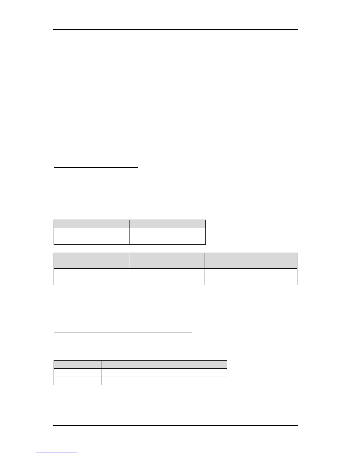
CPU FSB Bandwidth
800MHz 6.4GB/s
533MHz 4.2GB/s
Memory Frequency
Dual Channel DDR
Bandwidth
Single Channel DDR
Bandwidth
400MHz 6.4GB/s 3.2GB/s
333MHz 5.4GB/s 2.7GB/s
Note:
To maintain system stability, don’t change any of DRAM parameters in BIOS setup
to upgrade your system performance without acquiring technical information.
Memory frequency / CPU FSB synchronization
RUBY-9712VG2A support different memory frequencies depending on the CPU
front side bus and the type of DDR DIMM.
CPU FSB Memory Frequency
800MHz 400MHz
533MHz 333MHz
Page 29

System Installation
RUBY-9712VG2A User’s Manual 3-4
3.3 CompactFlash Card
RUBY-9712VG2A reserves one Type II CompactFlash socket for installing
CompactFlash card up to 1GB.
Installing CF
1) To protect your card, always hold it by the edges. Holding the center of the card
probably won’t damage it, but holding the card by the edges provides an extra
measure of protection.
2) Slide CompactFlash card into the socket.
3) If CompactFlash card doesn’t slide into the socket easily, don’t try to force it. It
won’t fit if you install it backwards. Turn it around and try inserting it again.
WARNING
1) Keep CompactFlash card away from direct sunlight, moisture, and magnetic
fields.
2) The True IDE mode does not support hot insertion and removal because of the
probable disruption of signals on the system bus.
3.4 Installing the Single Board Computer
To install your RUBY-9712VG2A into standard chassis or proprietary environment,
you need to perform the following:
Step 1: Check all jumpers setting on proper position.
Step 2: Install and configure CPU and memory module on right position.
Step 3: Place RUBY-9712VG2A into the dedicated position in your system.
Step 4: Attach cables to existing peripheral devices and secure it.
WARNING
Bus Interface Fully complies with PCI Local Bus specification V2.3 (support 4 master
PCI slots).
Note:
Please refer to section 3.4.1 to 3.4.4 to install INF/VGA/LAN/Audio drivers.
Page 30
System Installation
RUBY-9712VG2A User’s Manual 3-5
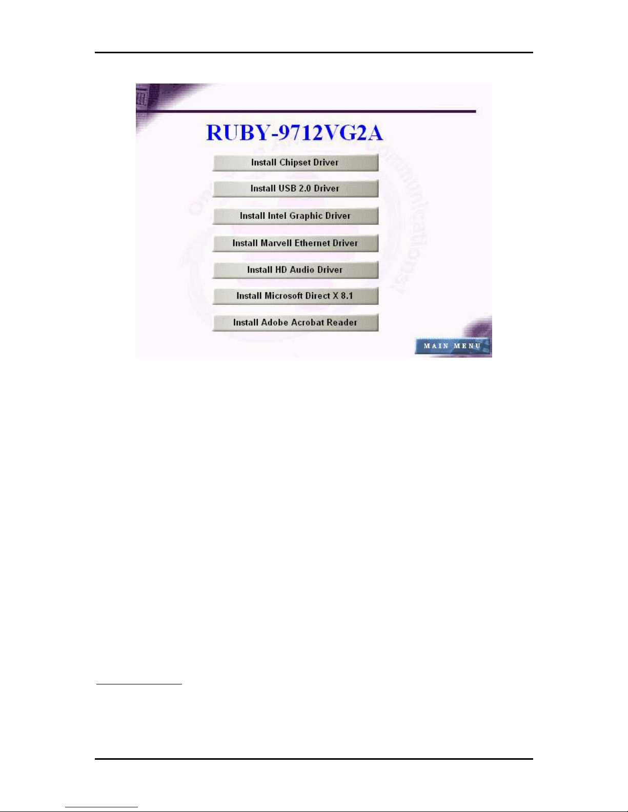
3.4.1 Chipset Component Driver
The chipset on RUBY-9712VG2A is a new chipset that a few old operating systems
might not be able to recognize. To overcome this compatibility issue, for Windows
Operating Systems such as Windows 98SE /2000 /XP / Server 2003, please install its
INF before any of other Drivers are installed. You can find very easily this chipset
component driver in RUBY-9712VG2A CD-title.
3.4.2 Intel Integrated Graphics GMCH Chip
Using GMCH High performance graphic integrated chipset is aimed to gain an
outstanding graphic performance. Shared 64 accompany it to 160MB system DDRSDRAM with Total Graphics Memory. This combination makes RUBY-9712VG2A an
excellent piece of multimedia hardware.
With no additional video adaptor, this onboard video will usually be the system
display output. By adjusting the BIOS setting to disable on-board VGA, an add-on
PCI VGA Card can take over the system display.
Drivers Support
Please find 82915G/GV/910GL GMCH driver in the RUBY-9712VG2A CD-title.
Drivers support Windows 2000 / XP.
Page 31
System Installation
RUBY-9712VG2A User’s Manual 3-6
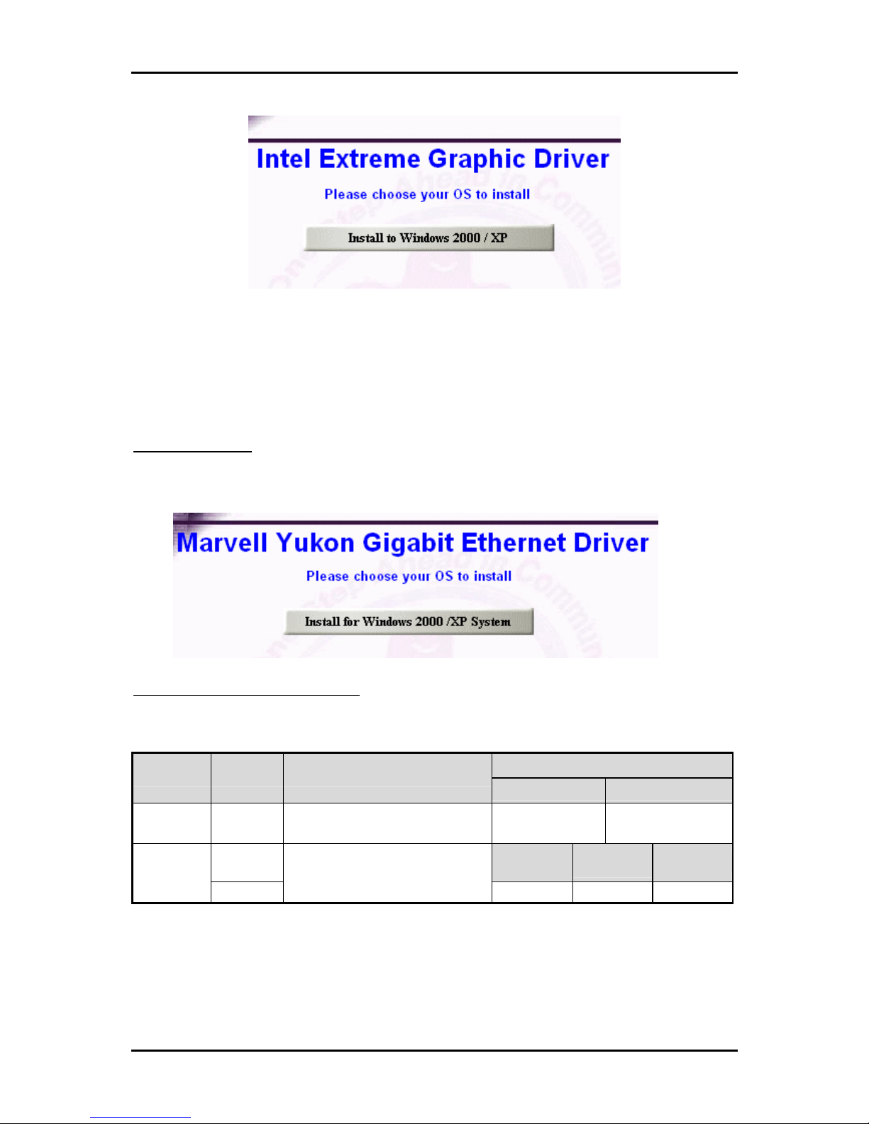
Windows-2000/XP: Please execute Install to Windows 2000 / XP System file to start
graphics driver installation.
3.4.3 On-board Fast Ethernet Controller
Drivers Support
Please find Marvell 88E8053 Gigabit LAN driver in /Ethernet directory of RUBY9712VG2A CD-title. The drivers support Windows 2000 / XP.
LED Indicator (for LAN status)
RUBY-9712VG2A provides three LED indicators to report Marvell 88E8053 Fast
Ethernet interfaces status. Please refer to the table below as a quick reference guide.
Operation of Ethernet Port
82541GI Color Name of LED
ON OFF
Status
LED
Green LAN Linked & Active LED Linked
Active
(Blinking)
Orange
Giga
Mbps
100 Mbps
10 Mbps
Speed
LED
Green
LAN speed LED
Orange Green Off
Page 32
System Installation
RUBY-9712VG2A User’s Manual 3-7
3.4.4 On-board AC-97 Audio Device
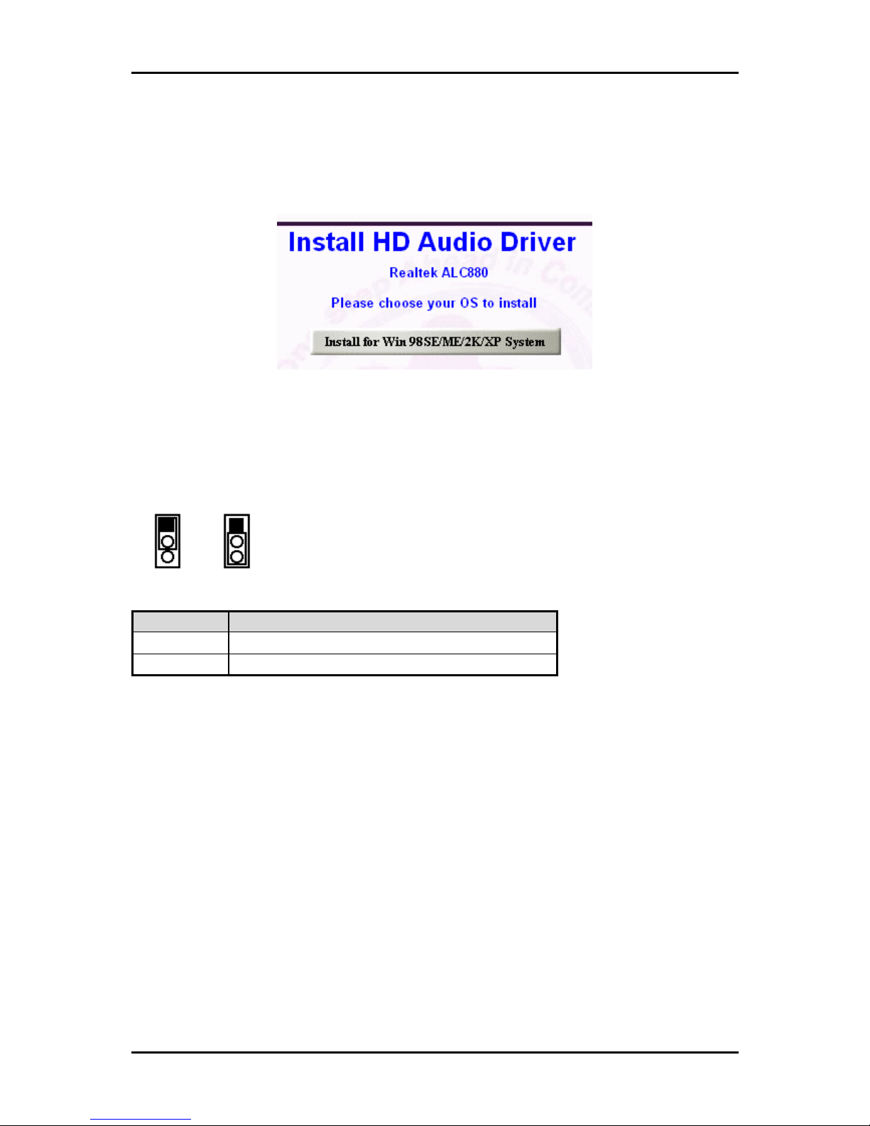
Please find Realtek ALC880AC’97 Audio driver of RUBY-9712VG2A CD-title. The
drivers support Windows 98SE / ME / 2000 / XP.
3.5 Clear CMOS Operation
The following table indicates how to enable/disable CMOS Clear Function hardware
circuit by putting jumpers at proper position.
Normal Clear
JP3 Function
1-2 Short Normal Operation ★
2-3 Short Clear CMOS contents
3.6 WDT Function
The working algorithm of the WDT function can be simply described as a counting
process. The Time-Out Interval can be set through software programming. The
availability of the time-out interval settings by software or hardware varies from
boards to boards.
RUBY-9712VG2A allows users control WDT through dynamic software
programming. The WDT starts counting when it is activated. It sends out a signal to
system reset or to non-maskable interrupt (NMI), when time-out interval ends. To
prevent the time-out interval from running out, a re-trigger signal will need to be
sent before the counting reaches its end. This action will restart the counting process.
A well-written WDT program should keep the counting process running under
normal condition. WDT should never generate a system reset or NMI signal unless
the system runs into troubles.
1
2
3
1
2
3
Page 33

System Installation
RUBY-9712VG2A User’s Manual 3-8
The related Control Registers of WDT are all included in the following sample
program that is written in C language. User can fill a non-zero value into the Timeout Value Register to enable/refresh WDT. System will be reset after the Time-out
Value to be counted down to zero. Or user can directly fill a zero value into Time-out
Value Register to disable WDT immediately. To ensure a successful accessing to the
content of desired Control Register, the sequence of following program codes should
be step-by-step run again when each register is accessed.
Additionally, there are maximum 2 seconds of counting tolerance that should be
considered into user’ application program. For more information about WDT, please
refer to Winbond W83627THF data sheet.
There are two PNP I/O port addresses that can be used to configure WDT,
1) 0x2E:EFIR (Extended Function Index Register, for identifying CR index number)
2) 0x2F:EFDR (Extended Function Data Register, for accessing desired CR)
Below are some example codes, which demonstrate the use of WDT.
// Enter Extended Function Mode
outp(0x002E, 0x87);
outp(0x002E, 0x87);
// Assign Pin 89 to be a WDTO
outp(0x002E, 0x2B);
outp(0x002F, inp(0x002F) & 0xEF);
// Select Logic Device 8
outp(0x002E, 0x07);
outp(0x002F, 0x08);
// Active Logic Device 8
outp(0x002E, 0x30);
outp(0x002F, 0x01);
// Select Count Mode
outp(0x002E, 0xF5);
outp(0x002F, (inp(0x002F) & 0xF7) | ( Count-mode Register & 0x08));
// Specify Time-out Value
outp(0x002E, 0xF6);
outp(0x002F, Time-out Value Register );
// Disable WDT reset by keyboard/mouse interrupts
outp(0x002E, 0xF7);
outp(0x002F, 0x00);
// Exit Extended Function Mode
outp(0x002E, 0xAA);
Page 34
System Installation
RUBY-9712VG2A User’s Manual 3-9
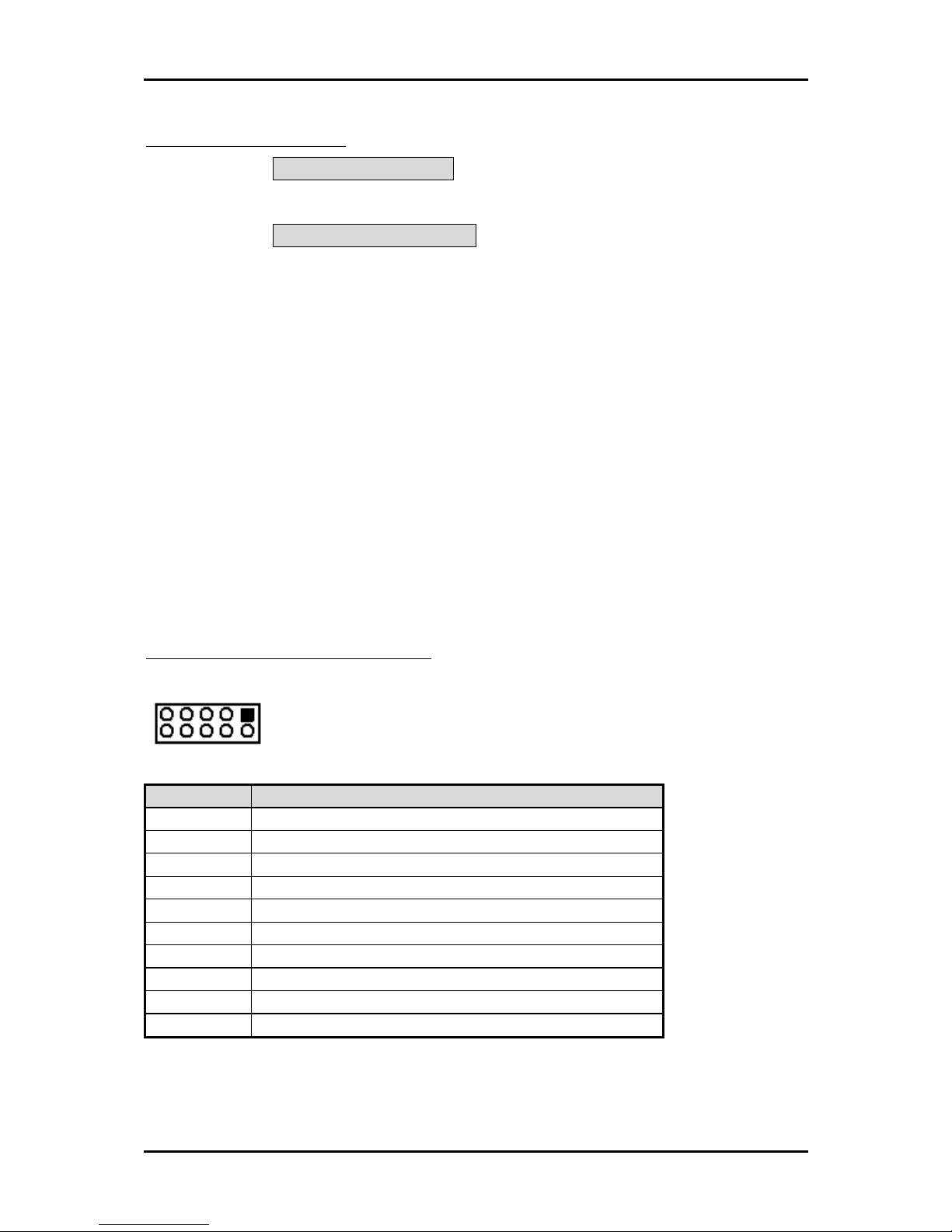
1 2 3 4 5
Definitions of Variables:
Value of Count-mode Register :
1) 0x00 -- Count down in seconds (Bit3=0)
2) 0x08 -- Count down in minutes (Bit3=1)
Value of Time-out Value Register :
1) 0x00 -- Time-out Disable
2) 0x01~0xFF -- Value for counting down
3.7 GPIO
The RUBY-9712VG2A provides 4 input/output ports that can be individually
configured to perform a simple basic I/O function. Users can configure each
individual port to become an input or output port by programming register bit of
I/O Selection. To invert port value, the setting of Inversion Register has to be made.
Port values can be set to read or write through Data Register.
Additionally, 4-extra Digital Output ports inversely amplified signals from GPIO
ports.
3.7.1 Pin assignment
J23: General Purpose I/O Connector
PIN No. Signal Description
1 General Purpose I/O Port 1 (GPIO1) SIO-GP26
2 General Purpose I/O Port 2 (GPIO2) SIO-GP25
3 General Purpose I/O Port 3 (GPIO3) SIO-GP24
4 General Purpose I/O Port 4 (GPIO4) SIO-GP23
5 Ground
6 Buffered Digital Output Port 1 (DO1) SIO-GP10
7 Buffered Digital Output Port 2 (DO2) SIO-GP11
8 Buffered Digital Output Port 3 (DO3) SIO-GP12
9 Buffered Digital Output Port 4 (DO4) SIO-GP13
10 +5V
Page 35

System Installation
RUBY-9712VG2A User’s Manual 3-10
3.7.2 Programming Guide
There are 4 GPIO pins & 4 DO on RUBY-9712VG2A. These GPIO pins are from
SUPER I/O (W83627THF) GPIO pins, and can be programmed as Input or Output
direction.
J23 pin header is for 4 GPIO pins & 4 DO and its pin assignment as following:
J23_Pin1=GPIO1: from SUPER I/O_GP26 with Ext. 4.7K PH
J23_Pin2=GPIO2: from SUPER I/O_GP25 with Ext. 4.7K PH
J23_Pin3=GPIO3: from SUPER I/O_GP24 with Ext. 4.7K PH
J23_Pin4=GPIO4: from SUPER I/O_GP23 with Ext. 4.7K PH
J23_Pin6=DO1: from SUPER I/O_GP10 with Ext. 4.7K PH
J23_Pin7=DO2: from SUPER I/O_GP11 with Ext. 4.7K PH
J23_Pin8=DO3: from SUPER I/O_GP12 with Ext. 4.7K PH
J23_Pin9=DO4: from SUPER I/O_GP13 with Ext. 4.7K PH
<<<<< Be careful Pin5=GND , Pin10=VCC >>>>>
There are several Configuration Registers (CR) of W83627THF needed to be
programmed to control the GPIO direction, and status (GPI)/value (GPO). CR00h ~
CR2F are common (global) registers to all Logical Devices (LD) in W83627THF.
CR07h contains the Logical Device Number that can be changed to access the LD as
needed. LD7 contains the GPIO10~17 registers.
Programming Guide:
Step1: CR2A_Bit [7.2]. P [1,1,1,1,1,1]; to select multiplexed pins as GPIO10~17 pins
Step2: LD7_CR07h.P [07h]; Point to LD7
Step3: LD7_CR30h_Bit0.P1; Enable LD7
Step4: Select GPIO direction, Get Status or output value.
LD7_CRF0h; GPIO17 ~ 10 direction, 1 = input, 0 = output pin
LD7_CRF2h.P [00h]; Let CRF1 (GPIO data port) non-invert to prevent from
confusion
LD7_CRF1h; GPIO17~10 data port, for input pin, get status from the related bit, for
output pin, write value to the related bit.
For example,
LD7_CRF0h_Bit4.P0; Let GPIO14 as output pin
LD7_CRF2h_Bit4.P0; Let CRF1_Bit4 non-inverted
LD7_CRF1h_Bit4.P0; Output “0” to GPIO14 pin (J23_Pin6)
LD7_CRF0h_Bit0.P1; Let GPIO10 as input pin
LD7_CRF2h_Bit0.P0; Let CRF1_Bit0 non-inverted
Read LD7_CRF1h_Bit0; Read the status from GPIO10 pin (J23_Pin1)
Page 36

System Installation
RUBY-9712VG2A User’s Manual 3-11
How to access W83627THF CR?
In RUBY-9712VG2A, the EFER = 002Eh, and EFDR = 002Fh.
EFER and EFDR are 2 IO ports needed to access W83627THF CR.
EFER is the Index Port, EFDR is the Data Port.
CR index number needs to be written into EFER first,
Then the data will be read/written from/to EFDR.
To R/W W83627THF CR, it is needed to Enter/Enable Configuration Mode first.
When completing the programming, it is suggested to Exit/Disable Configuration
Mode.
Enter Configuration Mode: Write 87h to IO port EFER twice.
Exit Configuration Mode: Write AAh to IO port EFER.
3.7.3 Example
Define GPIO4 as output pin, and output “0” to this pin.
mov dx,2eh ; Enter Configuration Mode
mov al,87h
out dx,al
jmp $+2
out dx,al
mov dx,2eh
mov al,2Ah ; Read CR2A
out dx,al
mov dx,2fh
in al,dx
or al,0FCh ; CR2A_Bit[7..2].P[1,1,1,1,1,1]
mov ah,al
mov dx,2eh
mov al,2Ah
out dx,al
mov dx,2fh
mov al,ah
out dx,al
Page 37

System Installation
RUBY-9712VG2A User’s Manual 3-12
mov dx,2eh
mov al,07h ; Point to LDN7
out dx,al
mov dx,2fh
mov al,07h
out dx,al
mov dx,2eh ; Read CR30
mov al,30h
out dx,al
mov dx,2fh
in al,dx
or al,01h
mov ah,al
mov dx,2eh ; CR30_Bit0.P1
mov al,30h
out dx,al
mov dx,2fh
mov al,ah
out dx,al
mov dx,2eh
mov al,0f0h ; Read LD7_CRF0
out dx,al
mov dx,2fh
in al,dx
and al,0efh
mov ah,al
mov dx,2eh
mov al,0f0h ; LD7_CRF0_Bit4.P0
out dx,al
mov dx,2fh
mov al,ah
out dx,al
mov dx,2eh
mov al,0f2h ; Read LD7_CRF2
out dx,al
mov dx,2fh
in al,dx
and al,0efh
mov ah,al
Page 38

System Installation
RUBY-9712VG2A User’s Manual 3-13
mov dx,2eh
mov al,0f2h ; LD7_CRF2_Bit4.P0
out dx,al
mov dx,2fh
mov al,ah
out dx,al
mov dx,2eh
mov al,0f1h ; Read LD7_CRF1
out dx,al
mov dx,2fh
in al,dx
and al,0efh
mov ah,al
mov dx,2eh
mov al,0f1h ; LD7_CRF1_Bit4.P0
out dx,al
mov dx,2fh
mov al,ah
out dx,al
mov dx,2eh ; Exit Configuration Mode
mov al,0AAh
out dx,al
Notes:
1) All the Buffered Digital Outputs are open-drain amplified form corresponding
GPIO ports.
2) Some other functions may occupy the lower nibble of the registers. Altering any
content in lower nibble will be undesired.
Page 39
BIOS Setup Information
RUBY-9712VG2A User’s Manual 4-1
Chapter 4
BIOS Setup Information
RUBY-9712VG2A is equipped with the AWARD BIOS stored in Flash ROM. These
BIOS has a built-in Setup program that allows users to modify the basic system
configuration easily. This type of information is stored in CMOS RAM so that it is
retained during power-off periods. When system is turned on, RUBY-9712VG2A
communicates with peripheral devices and checks its hardware resources against the
configuration information stored in the CMOS memory. If any error is detected, or
the CMOS parameters need to be initially defined, the diagnostic program will
prompt the user to enter the SETUP program. Some errors are significant enough to
abort the start-up.
4.1 Entering Setup
Turn on or reboot the computer. When the message “Hit <DEL> if you want to run
SETUP” appears, press <Del> key immediately to enter BIOS setup program.
If the message disappears before you respond, but you still wish to enter Setup,
please restart the system to try “COLD START” again by turning it OFF and then
ON, or touch the "RESET" button. You may also restart from “WARM START” by
pressing <Ctrl>, <Alt>, and <Delete> keys simultaneously. If you do not press
the keys at the right time and the system will not boot, an error message will be
displayed and you will again be asked to,
Press <F1> to Run SETUP or Resume
In HIFLEX BIOS setup, you can use the keyboard to choose among options or
modify the system parameters to match the options with your system. The table
below will show you all of keystroke functions in BIOS setup.
General Help
↑↓→ ←
: Move
Enter : Select
+ / - /PU /PD : Value
ESC : Exit
F1 : General Help
F2 : Item Help
F5 : Previous Values
F6 : Fail-Safe Defaults
F7 : Optimized Defaults
F9 : Menu in BIOS
F10 : Save
Page 40
BIOS Setup Information
RUBY-9712VG2A User’s Manual 4-2
4.2 Main Menu
Once you enter RUBY-9712VG2A AWARD BIOS CMOS Setup Utility, you should
start with the Main Menu. The Main Menu allows you to select from eleven setup
functions and two exit choices. Use arrow keys to switch among items and press
<Enter> key to accept or bring up the sub-menu.
Phoenix- AwardBIOS CMOS Setup Utility
f Standard CMOS Features
f Advanced BIOS Features
f Advanced Chipset Features
f Integrated Peripherals
f Power Management Setup
f PnP/PCI Configurations
f PC Health Status
f Frequency/Voltage Control
Load Fail-Safe Defaults
Load Optimized Defaults
Set Supervisor Password
Set User Password
Save & Exit Setup
Exit Without Saving
ESC : Quit F9 : Menu in BIOS ↑ ↓ → ← : Select Item
F10 : Save & Exit Setup
Time, Date, Hard Disk Type …
Note:
It is strongly recommended to reload Optimal Setting if CMOS is lost or BIOS is
updated.
Page 41
BIOS Setup Information
RUBY-9712VG2A User’s Manual 4-3
4.3 Standard CMOS Setup Menu
This setup page includes all the items in standard compatible BIOS. Use the arrow
keys to highlight the item and then use the <PgUp>/<PgDn> or <+>/<-> keys to
select the value or number you want in each item and press <Enter> key to certify it.
Follow command keys in CMOS Setup table to change Date, Time, Drive type, and
Boot Sector Virus Protection Status.
Phoenix- AwardBIOS CMOS Setup Utility
Standard CMOS Features
Item Help
Date (mm:dd:yy) Mon, Apr 25 2005
Time (hh:mm:ss) 15 : 19 : 30
f IDE Channel 0 Master [Maxtor 91021U2]
f IDE Channel 0 Slave [None]
f IDE Channel 1 Master [ST380817AS]
f IDE Channel 1 Slave [None]
Video [EVG/VGA]
Base Memory 640K
Extended Memory 252928K
Total Memory 253952K
Menu Level f
Change the day, month,
year and century
↑↓→←: Move Enter: Select +/-/PU/PD: Value F10: Save ESC: Exit F1: General Help
F5: Previous Values F6: Fail-Safe Defaults F7: Optimized Defaults
Note:
Setting On-Chip Serial ATA is Auto Mode.
Page 42
BIOS Setup Information
RUBY-9712VG2A User’s Manual 4-4
Menu Selections
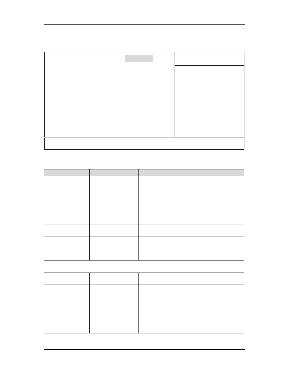
Item Options Description
Date mm:dd:yy Change the day, month, year and
century
Time hh:mm:ss Change the internal clock
IDE Channel 0
Master
Options are in its sub
menu
Press <Enter> to enter the sub menu of
detailed options
IDE Channel 0
Slave
Options are in its sub
menu
Press <Enter> to enter the next page for
detail hard drive settings
IDE Channel 1
Master
Options are in its sub
menu
Press <Enter> to enter the next page for
detail hard drive settings
IDE Channel 1
Slave
Options are in its sub
menu
Press <Enter> to enter the next page for
detail hard drive settings
Video EGA/VGA, CGA 40
CGA 80, MONO
Select the default video device
Base Memory 640K
Displays the amount of conventional
memory detected during boot up
Extended
Memory
N/A
Displays the amount of extended
memory detected during boot up
Total Memory N/A
Displays the total memory available in
the system
4.4 IDE Adaptors Setup Menu
The IDE adapters control the IDE devices, such as Hard disk drive or CDROM drive.
It uses a separate sub menu to configure each hard disk drive.
Phoenix- AwardBIOS CMOS Setup Utility
IDE Channel 0 Master
Item Help
IDE HDD Auto-Detection [Press Enter]
IDE Channel 0 Master [Auto]
Access Mode [Auto]
Capacity 10246 MB
Cylinder 19852
Head 16
Precomp 0
Landing Zone 19851
Sector 63
Menu Level f
To auto-detect the HDD’s
size, head … on this
channel
↑↓→←: Move Enter: Select +/-/PU/PD: Value F10: Save ESC: Exit F1: General Help
F5: Previous Values F6: Fail-Safe Defaults F7: Optimized Defaults
Page 43

BIOS Setup Information
RUBY-9712VG2A User’s Manual 4-5
Menu Selections
Item Options Description
IDE HDD Autodetection
Press Enter Press Enter to auto-detect the HDD on
this channel. If detection is
successful, it fills the remaining fields
on this menu.
IDE Channel 0
Master
None
Auto
Manual
Selecting ‘manual’ lets you set the
remaining fields on this screen. Selects
the type of fixed disk. "User Type" will
let you select the number of cylinders,
heads, etc.
Note: PRECOMP=65535 means NONE!
Access Mode CHS
LBA
Large
Auto
Choose the access mode for this hard
disk
Capacity Auto Display your disk
drive size
Disk drive capacity (Approximated).
Note that this size is usually slightly
greater than the size of a formatted
disk given by a disk-checking
program.
The following options are selectable only if the ‘IDE Primary Master’ item is set to
‘Manual’
Cylinder Min = 0
Max = 65535
Set the number of cylinders for this
hard disk.
Head Min = 0
Max = 255
Set the number of read/write heads
Precomp Min = 0
Max = 65535
**** Warning: Setting a value of 65535
means no hard disk
Landing zone Min = 0
Max = 65535
****
Sector Min = 0
Max = 255
Number of sectors per track
Page 44
BIOS Setup Information
RUBY-9712VG2A User’s Manual 4-6
Phoenix- AwardBIOS CMOS Setup Utility
IDE Channel 1 Master
Item Help
IDE HDD Auto-Detection [Press Enter]
IDE Channel 1 Master [Auto]
Access Mode [Auto]
Capacity 80GB
Cylinder 38309
Head 16
Precomp 0
Landing Zone 38308
Sector 255
Menu Level f
To atuo-detect the HDD’s
size, head … on this
channel
↑↓→←: Move Enter: Select +/-/PU/PD: Value F10: Save ESC: Exit F1: General Help
F5: Previous Values F6: Fail-Safe Defaults F7: Optimized Defaults
Menu Selections
Item Options Description
IDE HDD Autodetection
Press Enter Press Enter to auto-detect the HDD on this
channel. If detection is successful, it fills the
remaining fields on this menu.
IDE Channel 1
Master
None
Auto
Manual
Selecting ‘manual’ lets you set the remaining
fields on this screen. Selects the type of fixed
disk. "User Type" will let you select the
number of cylinders, heads, etc.
Note: PRECOMP=65535 means NONE!
Access Mode CHS, LBA
Large, Auto
Choose the access mode for this hard disk
Capacity Auto Display your
disk drive size
Disk drive capacity (Approximated). Note
that this size is usuall
y
slightly greater than the
size of a formatted disk given by a diskchecking program.
The following options are selectable only if the ‘IDE Primary Master’ item is set to
‘Manual’
Cylinder Min = 0
Max = 65535
Set the number of cylinders for this hard disk
Head Min = 0
Max = 255
Set the number of read/write heads
Precomp Min = 0
Max = 65535
**** Warning: Setting a value of 65535 means
no hard disk
Landing zone Min = 0
Max = 65535
****
Sector Min = 0
Max = 255
Number of sectors per track
Page 45
BIOS Setup Information
RUBY-9712VG2A User’s Manual 4-7
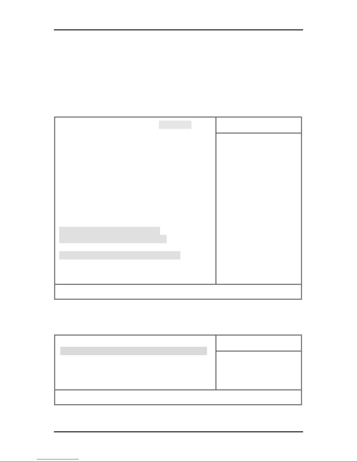
4.5 Advanced BIOS Feature
This section allows you to configure your system for basic operation. You have the
opportunity to select the system’s default speed, boot-up sequence, keyboard
operation, shadowing and security.
Phoenix- AwardBIOS CMOS Setup Utility
Advanced BIOS Features
Item Help
f CPU Feature [Press Enter]
f Hard Disk Boot Priority [Press Enter]
Virus Warning [Disabled]
CPU L1 & L2 Cache [Enabled]
Hyper-Threading Technology [Enabled]
Quick Power On Self Test [Enabled]
First Boot Device [Hard Disk]
Second Boot Device [CDROM]
Third Boot Device [ZIP100]
Boot Other Device [Enabled]
Boot up NumLock Status [On]
Gate A20 Option [Normal]
Typematic Rate Setting [Disabled]
X Typematic Rate (Chars/Sec) 6
X Typematic Delay (Msec) 250
Security Option [Setup]
X APIC Mode Enabled
MPS Version Control For OS [1.4]
OS Select For DRAM > 64MB [Non-OS2]
Small Logo(EPA) Show [Disabled]
Menu Level f
↑↓→←: Move Enter: Select +/-/PU/PD: Value F10: Save ESC: Exit F1: General Help
F5: Previous Values F6: Fail-Safe Defaults F7: Optimized Defaults
Phoenix- AwardBIOS CMOS Setup Utility
CPU Feature
Item Help
Delay Prior to Thermal [16 Min]
Thermal Management Thermal Monitor 1
Limit CPUID MaxVal [Disabled]
Menu Level f
↑↓→←: Move Enter: Select +/-/PU/PD: Value F10: Save ESC: Exit F1: General Help
F5: Previous Values F6: Fail-Safe Defaults F7: Optimized Defaults
Page 46
BIOS Setup Information
RUBY-9712VG2A User’s Manual 4-8
Delay Prior to Thermal
The choice: 4 Min, 8 Min, 16 Min, and 32 Min.
Limit CPUID Maxval
Set Limit CPUID MaxVal to 3, Should Be “Disabled” for WinXP.
Enabled
For OS: Windows NT4.0 Install.
Disabled
For OS: Windows XP Install.
Phoenix- AwardBIOS CMOS Setup Utility
Hard Disk Boot Priority
Item Help
1. ch0 M. : Maxtor 91021U2
2. ch1 M. : ST380817AS
3. Bootable add-in Cards
Menu Level f
Use <↑> or <↓> to select a
device, then press <+> to
move it up, or <-> to move
it down the list. Press
<ESC> to exit this menu.
↑↓→←: Move Enter: Select +/-/PU/PD: Value F10: Save ESC: Exit F1: General Help
F5: Previous Values F6: Fail-Safe Defaults F7: Optimized Defaults
Hard Disk Boot Priority
Select Hard Disk Boot Device Priority. Use <↑> or <↓> to select a device, then
press <+> to move it up, or <-> to move it down the list. Press <ESC> to exit this
menu.
Bootable Add-in Cards Select SCSI Boot
Ch x M (S). Select IDE Channel 0,1 Master or Salve Boot
Ch x M. Select IDE Channel 2 or 3 Master Boot
Virus Warning
Allow you to choose the VIRUS warning feature for IDE Hard Disk boot sector
protection. If this function is enabled and someone attempt to write data into this
area, BIOS will show a warning message on screen and alarm beep.
Enabled
Activates automatically when the system boots up causing a
warning message to appear when anything attempts to access the
boot sector or hard disk partition table.
Disabled
No warning message will appear when anything attempts to access
the boot sector or hard disk partition table.
Page 47

BIOS Setup Information
RUBY-9712VG2A User’s Manual 4-9
CPU L1 Cache/L2 Cache
These two categories speed up memory access. However, it depends on
CPU/chipset design.
Enabled Enable Cache
Disabled Disable Cache
Hyper-Threading Technology
“Enabled” for Windows XP and Linux 2.4.X (OS optimized for Hyper-Threading
Technology and “Disabled” for other OS (OS not optimized for Hyper-Threading
Technology).
The choice: Enabled, Disabled.
Quick Power On Self Test
Allows the system to skip certain tests while booting. This will decrease the time
needed to boot the system.
Enabled Enable quick POST
Disabled Normal POST
First/Second/Third Boot Device
Select your boot device priority.
The choice: LS120, Hard Disk, CDROM, ZIP100, USB-FDD, USB-ZIP, USB-CDROM,
LAN and Disabled.
Boot Other Device
Select your boot device priority.
The choice: Enabled, Disabled.
Boot Up NumLock Status
Select power on state for NumLock.
The choice: Off, On.
Gate A20 Option
Fast-lets chipsets control Gate A20 and Normal – a pin in the keyboard controller
controls Gate A20. Default is Fast.
The choice: Normal, Fast.
Page 48
BIOS Setup Information
RUBY-9712VG2A User’s Manual 4-10
Typematic Rate Setting
Keystrokes repeat at a rate determined by the keyboard controller – When enabled,
the typematic rate and typematic delay can be selected.
The choice: Enabled, Disabled.
Typematic Rate (Chars/sec)
The rate at which character repeats when you hold down a key.
The choice: 6, 8, 10, 12, 15, 20, 24, and 30.
Typematic delay (Msec)
The delay before keystrokes begin to repeat.
The choice: 250, 500, 750, and 1000.
Security Option
Select whether the password is required every time the system boots or only when
you enter setup.
System
The system will not boot and access to Setup will be denied if the
correct password is not entered at the prompt.
Setup
The system will boot, but access to Setup will be denied if the
correct password is not entered at the prompt.
APIC Mode
Setting to Enabled can cause instabilities. Once the operating system is installed,
such as Windows XP in my case, this setting cannot be changed without reinstalling
the operating system, regardless of whether the initial setting is Disabled or Enabled.
The purpose of setting it to Enabled is to extend the number of IRQ's, which sounds
like a real risky proposition. I'm not surprised to see the conclusion reached at APIC:
Benefit or Trouble. The number of IRQ's should be fine without being extended,
anyway.
The choice: Enabled, Disabled.
MPS Version Control For OS
Not changeable with APIC Mode set to disabled.
The choice: 1.1, 1.4.
Page 49
BIOS Setup Information
RUBY-9712VG2A User’s Manual 4-11
OS Select For DRAM > 64MB
Select OS/2 only if you are running SO/2 operating system with greater than 64MB
of RAM on the system.
The choice: Non-OS2, OS2.
Small Logo (EPA) Show
The choice: Enabled, Disabled.
4.6 Advanced Chipset Feature
This section allows you to configure the system based on the specific features of the
Intel 915GV chipset. This chipset manages bus speeds and access to system
memory resources, such as DRAM (DDR SDRAM) and the external cache. It also
coordinates communications between the conventional PCI Express bus and PCI
bus. It must be stated that these items should never need to be altered. The
default settings have been chosen because they provide the best operating conditions
for your system. The only time you might consider making any changes would be
if you discovered that data was being lost while using your system.
Phoenix- AwardBIOS CMOS Setup Utility
Advanced Chipset Features
Item Help
DRAM Timing Selectable [By SPD]
X CAS Latency Time 3
X DRAM RAS# to CAS# Delay 4
X DRAM RAS# Precharge 4
X Precharge delay (tRAS) 8
X System Memory Frequency 400MHZ
SLP_S4# Assertion Width [4 to 5 Sec.]
System BIOS Cacheable [Enabled]
Video BIOS Cacheable [Enabled]
Memory Hole At 15M-16M [Disabled]
f PCI Express Root Port Func [Press Enter]
** VGA Setting **
On-Chip Video Memory Size [Press Enter]
On-Chip Frame Buffer Size 8MB
FIXED Memory Size 0MB
DVMT Memory Size 120MB
Boot Display [Auto]
Menu Level f
↑↓→←: Move Enter: Select +/-/PU/PD: Value F10: Save ESC: Exit F1: General Help
F5: Previous Values F6: Fail-Safe Defaults F7: Optimized Defaults
Page 50

BIOS Setup Information
RUBY-9712VG2A User’s Manual 4-12
This chipset settings deal with CPU access to dynamic random access memory
(DRAM). The default timings have been carefully chosen and should only be altered
if data is being lost. Such a scenario might well occur if your system had mixed
speed DRAM chips installed so that greater delays may be required to preserve the
integrity of the data held in the slower memory chips.
DRAM Timing Selectable
This option provides DIMM plug-and-play support by serial presence detect (SPD)
mechanism via the system management bus (SMBUS) interface.
The choice: Manual, By SPD.
CAS Latency Time
This option controls the number of SCLKs between the time a read command is
sampled by the DRAMs and the time the GMCH samples correspondent data from
the DRAMs.
The choice: 2, 2.5, 3, Auto.
DRAM RAS# to CAS# Delay
This option controls the number of SCLKs (SDRAM Clock) from a row activate
command to a read or write command. If your system installs good quality of
SDRAM, you can set this option to “3 SCLKs” to obtain better memory performance.
Normally, the option will be set to Auto.
The choice: 2, 3, 4, and 5, Auto.
DRAM RAS# Precharge
This option controls the number of SCLKs for RAS# precharge. If your system
installs good quality of SDRAM, you can set this option to “3 SCLKs” to obtain
better memory performance. It is set to auto normally.
The choice: 2, 3, 4, and 5, Auto.
Precharge delay (tRAS)
The choice: 4, 5, 6, 7, 8, 9, 10, 11, 12, 13, 14, and 15, Auto.
System Memory Frequency
Users are recommended to use Auto for memory frequency selection.
The choice: Auto, 333MHz, 400MHz.
Page 51

BIOS Setup Information
RUBY-9712VG2A User’s Manual 4-13
SLP_S4# Assertion Width
The choice: 4 to 5 Sec., 3to 4 Sec, 2 to 3 Sec., 1 to 2 Sec.
System BIOS Cacheable
Selecting Enabled allows caching of the system BIOS ROM at F0000h-FFFFFh,
resulting in better system performance. However, if any program writes to this
memory area, a system error may result.
The choice: Enabled, Disabled.
Video BIOS Cacheable
Select “Enabled” to enable caching VGA BIOS into L2 cache to get higher display
performance. “Disabled” to ignore this BIOS caching function.
The choice: Enabled, Disabled.
Memory Hole At 15-16M
In order to improve performance, certain space in memory is reserved for ISA cards.
This memory must be mapped into the memory space below 16MB.
The choice: Enabled, Disabled.
Phoenix- AwardBIOS CMOS Setup Utility
PCI Express Root Port Func
Item Help
PCI Express Port 1 [Auto]
PCI Express Port 2 [Auto]
PCI Express Port 3 [Auto]
PCI Express Port 4 [Auto]
PCI-E Compliancy Mode [V1.0a]
Menu Level f
↑↓→←: Move Enter: Select +/-/PU/PD: Value F10: Save ESC: Exit F1: General Help
F5: Previous Values F6: Fail-Safe Defaults F7: Optimized Defaults
PCI Express Port 1 / Port 2 / Port 3 / Port 4
The choice: Auto, Enabled, Disabled.
PCI-E Compliancy Mode
The choice: V1.0 / V1.0a.
Page 52
BIOS Setup Information
RUBY-9712VG2A User’s Manual 4-14
On-Chip Video Memory Size
The choice: Press Enter.
Pre- Fixed DVMT Fixed+DVMT Total Graphics
Allocated Memory
1MB 63MB 0MB NA 64MB
1MB 0MB 63MB NA 64MB
1MB 127MB 0MB NA 128MB
1MB 0MB 127MB NA 128MB
1MB 0MB 0MB 63MB+64MB 128MB
1MB 0MB MAX. DVMT NA 160MB
8MB 56MB 0MB NA 64MB
8MB 0MB 56MB NA 64MB
8MB 120MB 0MB NA 128MB
8MB 0MB 120MB NA 128MB
8MB 0MB 0MB 56MB+64MB 128MB
8MB 0MB MAX. DVMT NA 160MB
↑↓: Move ENTER: Accept ESC: Abort
Boot Display
The choice: Auto, CRT.
4.7 Integrated Peripherals
Phoenix- AwardBIOS CMOS Setup Utility
Integrated Peripherals
Item Help
f OnChip IDE Device [Press Enter]
f Onboard Device [Press Enter]
f Super IO Device [Press Enter]
Menu Level f
↑↓→←: Move Enter: Select +/-/PU/PD: Value F10: Save ESC: Exit F1: General Help
F5: Previous Values F6: Fail-Safe Defaults F7: Optimized Defaults
Page 53
BIOS Setup Information
RUBY-9712VG2A User’s Manual 4-15
Phoenix- AwardBIOS CMOS Setup Utility
OnChip IDE Device
Item Help
IDE HDD Block Mode [Enabled]
IDE DMA transfer access [Enabled]
On-Chip Primary PCI IDE [Enabled]
IDE Primary Master PIO [Auto]
IDE Primary Slave PIO [Auto]
IDE Primary Master UDMA [Auto]
IDE Primary Slave UDMA [Auto]
On-Chip Secondary PCI IDE [Enabled]
IDE Secondary Master PIO [Auto]
IDE Secondary Slave PIO [Auto]
IDE Secondary Master UDMA [Auto]
IDE Secondary Slave UDMA [Auto]
*** On-Chip Serial ATA Setting ***
On-Chip Serial ATA [Disabled]
X PATA IDE Mode Primary
SATA Port P1, P3 is Secondary
Menu Level f
If your IDE hard drive
supports block mode
select Enabled for
automatic detection of the
optimal number of block
read/writes per sector the
drive can support.
↑↓→←: Move Enter: Select +/-/PU/PD: Value F10: Save ESC: Exit F1: General Help
F5: Previous Values F6: Fail-Safe Defaults F7: Optimized Defaults
IDE HDD Block Mode
If your IDE hard drive supports block mode select Enabled for automatic detection
of the optimal number of block read/writes per sector the drive can support.
The choice: Enabled, Disabled.
IDE DMA transfer access
The choice: Enabled, Disabled.
On-Chip Primary/Secondary PCI IDE
The chipset contains a PCI IDE interface with support for two IDE channels. Select
Enabled to activate the primary IDE interface. Select Disabled to deactivate this
interface.
The choice: Enabled, Disabled.
Page 54
BIOS Setup Information
RUBY-9712VG2A User’s Manual 4-16
IDE Primary/Secondary Master/Slave PIO
The four IDE PIO (Programmed Input/Output) fields let you set a PIO mode (0-4)
for each of the four IDE devices that the onboard IDE interface supports. Modes 0
through 4 provide successively increased performance. In Auto mode, the system
automatically determines the best mode for each device.
The choice: Auto, Mode 0, Mode 1, Mode 2, Mode 3, and Mode 4.
IDE Primary/Secondary Master/Slave UDMA
Ultra DMA/33/66/100 implementation is possible only if your IDE hard drive
supports it and the operating environment includes a DMA driver (Windows 95
OSR2 or a third-party IDE bus master driver). If your hard drive and your system
software both support Ultra DMA/33/66/100, select Auto to enable BIOS support.
The choice: Auto, Disabled.
On-Chip Serial ATA
Disabled Disabled SATA Controller.
Auto Auto arrange by BIOS.
Combined Mode
PATA and SATA are combined. Max. Of 2 IDE drives in each
channel.
Enhanced Mode
Enable both SATA and PATA. Max. Of 6 IDE drives are
Supported.
SATA Only SATA is operating in legacy mode.
Phoenix- AwardBIOS CMOS Setup Utility
Onboard Device
Item Help
USB Controller [Enabled]
USB 2.0 Controller [Enabled]
USB Keyboard Support [Enabled]
USB Mouse Support [Disabled]
Azalia AC97 Audio Select [Auto]
Menu Level f
↑↓→←: Move Enter: Select +/-/PU/PD: Value F10: Save ESC: Exit F1: General Help
F5: Previous Values F6: Fail-Safe Defaults F7: Optimized Defaults
USB Controller
This item allows you to enable/disable USB (Universal Serial Bus) function.
The choice: Enabled, Disabled.
Page 55
BIOS Setup Information
RUBY-9712VG2A User’s Manual 4-17
USB 2.0 Controller
This entry is for disable/enable EHCI controller only. This BIOS itself may/may
not have high speed USB support built in, the support will be automatically turn on
when high speed device were attached.
The choice: Enabled, Disabled.
USB Keyboard Support
This item allows you to enable USB keyboard function under POST, BIOS setup
menu, DOS, or Windows-NT with no USB driver loaded.
The choice: Enabled, Disabled.
USB Mouse Support
This item allows you to enabled USB Mouse function under POST, BIOS Setup
menu, DOS, or Window-NT with no USB driver loaded.
The choice: Enabled, Disabled.
Azalia AC97 Audio Select
Users can enable or disable on board AC97 Audio Function.
The choice: Enabled, Disabled.
Phoenix- AwardBIOS CMOS Setup Utility
Super IO Device
Item Help
POWER ON Function [BUTTON ONLY]
X KB Power ON Password Enter
X Hot Key Power ON Ctrl-F1
Onboard Serial Port 1 [3F8/IRQ4]
Onboard Serial Port 2 [2F8/IRQ3]
UART Mode Select [Normal]
X RxD, TxD Active Hi, Lo
X IR Transmission Delay Enabled
X UR2 Duplex Mode Half
X Use IR Pins IR-Rx2Tx2
Onboard Parallel Port [378/IRQ7]
Parallel Port Mode [SPP]
X EPP Mode Select EPP1.7
X ECP Mode Use DMA 3
PWRON After PWR-Fail [Off]
Menu Level f
↑↓→←: Move Enter: Select +/-/PU/PD: Value F10: Save ESC: Exit F1: General Help
F5: Previous Values F6: Fail-Safe Defaults F7: Optimized Defaults
Page 56
BIOS Setup Information
RUBY-9712VG2A User’s Manual 4-18
Power On Function
This item allows you to select different power on scheme using ATX power supply.
Password
Power on using customized password string
Hot Key
Power on using special customized key
Mouse Left
Power on using mouse left click
Mouse Right
Power on using mouse right click
Any Key
Power on using any keyboard key
Button Only
Power on by power Button
Keyboard 98
Power on by keyboard 98 [Only power ON/OFF key]
Keyboard Power On Password
In the event of “Power On Function” being configured as “Password”, this item will
be enabled for tuning. Press “Enter” key to enter a customized password, and
confirm again when being asked. In the case that the confirmed password does not
match the configured one, the message of “Password Disabled – Press any key to
continue…” will be prompted.
Hot Key Power On
In the event of “Power On Function” being configured as “Hot Key”, this item will
be enabled for tuning.
The choice: Ctrl-F1 to Ctrl-F12.
Onboard Serial Port 1/Port 2
Select an address and corresponding interrupt for the first and second serial ports.
The choice: Disabled, 3F8/IRQ4, 2F8/IRQ3, 3E8/IRQ4, 2E8/IRQ3, Auto.
UART Mode Select
This item allows users to select Infrared transmission mode.
Normal
Disable Infrared function
IrDA
Select IrDA mode transmission
ASKIR
Select ASKIR mode transmission
RxD, TxD Active
This item is to configure Infrared transmission rate. Four options are available:
Hi, Hi
High rate for receiving / High rate for transmitting
Hi, Lo
High rate for receiving / Low rate for transmitting
Lo, Hi
Low rate for receiving / High rate for transmitting
Lo, Lo
Low rate for receiving / Low rate for transmitting
Page 57
BIOS Setup Information
RUBY-9712VG2A User’s Manual 4-19
IR Transmission Delay
This option will be available when IR is enabled.
The choice: Enabled, Disabled.
UR2 Duplex Mode
The available choices are full duplex mode and half duplex mode
The choice: Full, Half.
Use IR Pins
The available choices are IR-Rx2Tx2/ RxD2, TxD2.
The choice: IR-Rx2Tx2 / RxD2, TxD2.
Onboard Parallel Port
This item allows you to configure I/O address of the onboard parallel port.
The choice: Disabled, 378/IRQ7, 278/IRQ5, and 3BC/IRQ7.
Parallel Port Mode
There are four different modes for the onboard parallel port :
SPP
Switch to SPP mode
EPP
Switch to EPP mode
ECP
Switch to ECP mode
ECP + EPP
Switch to ECP + EPP mode
Normal
Switch to Normal mode
EPP Mode Select
Select different version of EPP mode.
The choice: EPP1.7, EPP1.9.
ECP Mode Use DMA
Select a proper DMA channel for ECP mode.
The choice: 1, 3.
Page 58
BIOS Setup Information
RUBY-9712VG2A User’s Manual 4-20
PWRON After PWR-Fail
This item allows user to configure the power status of using ATX power supply after
a serious power loss occurs.
On
System automatically restores power back
Off
System stays at power –off
4.8 Power Management Setup
The Power Management Setup allows you to configure you system to most
effectively save energy while operating in a manner consistent with your own style
of computer use.
Phoenix- AwardBIOS CMOS Setup Utility
Power Management Setup
Item Help
ACPI Function [Enabled]
ACPI Suspend Type [S1(POS)]
X Run VGABIOS if S3 Resume No
Power Management [User Define]
Video Off Method [DPMS]
Video Off In Suspend [Yes]
Suspend Type [Stop Grant]
Suspend Mode [Disabled]
HDD Power Down [Disabled]
Soft-Off by PWR-BTTN [Instant-Off]
Wake-up by On Board LAN [Disabled]
Power On by Ring [Disabled]
X USB KB Wake-Up From S3 Disabled
Resume by Alarm [Disabled]
X Date(of Month) Alarm 0
X Time(hh:mm:ss) Alarm 0 : 0 :0
** Reload Global Timer Events **
Primary IDE 0 [Disabled]
Primary IDE 1 [Disabled]
Secondary IDE 0 [Disabled]
Secondary IDE 1 [Disabled]
FDD,COM,LPT Port [Disabled]
PCI PIRQ[A-D]# [Disabled]
Menu Level f
↑↓→←: Move Enter: Select +/-/PU/PD: Value F10: Save ESC: Exit F1: General Help
F5: Previous Values F6: Fail-Safe Defaults F7: Optimized Defaults
Page 59
BIOS Setup Information
RUBY-9712VG2A User’s Manual 4-21
ACPI Function
This item allows you to enable/disable the Advanced Configuration and Power
Management (ACPI).
The choice: Enabled, Disabled.
ACPI Suspend Type
To decide which ACPI suspend mode to use.
The choice: S1(POS), S3(STR).
Run VGA BIOS if S3 Resume
The choice: Auto, Yes, No.
Power Management
This category allows you to select the type (or degree) of power saving and is
directly related to “HDD Power Down”, “Suspend Mode”.
There are three selections for Power Management, three of which have fixed mode
settings.
Min. Power Saving
Minimum power management. Suspend Mode = 1 Hour,
and HDD Power Down = 15 Min.
Max. Power Saving
Maximum power management. Suspend Mode = 1 Min.,
and HDD Power Down = 1 Min.
User Defined
Allow you to set each mode individually. When not
disabled, Suspend Mode ranges from 1 min. to 1 Hour and
HDD Power Down ranges from 1 Min. to 15 Min.
Video Off Method
This determines the manner in which the monitor is blanked.
V/H SYNC+Blank
This selection will cause the system to turn off the vertical
and horizontal synchronization ports and write blanks to
the video buffer.
Blank Screen
This option only writes blanks to the video buffer.
DPMS
Initial display power management signaling.
Video Off In Suspend
This allows user to enable/disable video off in Suspend Mode.
The choice: Yes, No.
Page 60

BIOS Setup Information
RUBY-9712VG2A User’s Manual 4-22
Suspend Type
Two options are available: Stop Grant and PwrOn Suspend.
The choice: Stop Grant, PwrOn Suspend.
Suspend Mode
When enabled and after the set time of system inactivity, all devices except the CPU
will be shut off.
The choice: Disabled, 1 Min, 2 Min, 4 Min, 8 Min, 12 Min, 20 Min, 30 Min, 40 Min,
and 1 Hour.
HDD Power Down
When enabled and after the set time of system inactivity, the hard disk drive will be
powered down while all other devices remain active.
The choice: Disabled, 1 Min, 2 Min, 3 Min, 4 Min, 5 Min, 6 Min, 7 Min, 8 Min, 9 Min,
10 Min, 11 Min, 12 Min, 13 Min, 14 Min, 15 Min.
Soft-Off by PWR-BTTN
This item allows users to set the time to remove the power after the power button is
pressed.
The choice: Instant-Off, Delay 4 Sec.
Wake-Up by On Board LAN
This option can be enabled to support Wake Up by on-board LAN.
The choice: Disabled, Enabled.
Power On by Ring
When select “Enabled”, a system that is at soft-off mode will be alert to Wake-OnModem signal.
The choice: Enabled, Disabled.
USB KB Wake-up From S3
The choice: Enabled, Disabled.
Page 61

BIOS Setup Information
RUBY-9712VG2A User’s Manual 4-23
Resume by Alarm
This item allows users to enable/disable the resume by alarm function. When
“Enabled” is selected, system using ATX power supply could be powered on if a
customized time and day is approached.
The choice: Enabled, Disabled.
Date(of Month) Alarm
When “Resume by Alarm” is enabled, this item could allow users to configure the
date parameter of the timing dateline on which to power on the system.
The choice: 0 ~ 31.
Time(hh:mm:ss) Alarm
When “Resume by Alarm” is enabled, this item could allow users to configure the
time parameter of the timing dateline on which to power on the system.
The choice: hh (0~23), mm (0~59), ss (0 ~59).
Primary/Secondary IDE 0/1
This item is to configure IDE devices being monitored by system so as to keep
system out of suspend mode if the associated device is busy.
The choice: Enabled, Disabled.
FDD, COM, LPT Port
This item is to configure floppy device, COM ports, and parallel port being
monitored by system so as to keep system out of suspend mode if the associated
device is busy.
The choice: Enabled, Disabled.
PCI PIRQ[A-D]#
This option can be used to detect PCI device activities. If they are activities, the
system will go into sleep mode.
The choice: Enabled, Disabled.
Page 62

BIOS Setup Information
RUBY-9712VG2A User’s Manual 4-24
4.9 PnP/PCI Configurations
This section describes configuring the PCI bus system. PCI, or Personal Computer
Interconnect, is a system, which allows I/O devices to operate at speeds nearing the
speed the CPU itself, uses when communicating with its own special components.
This section covers some very technical items and it is strongly recommended that
only experienced users should make any changes to the default settings.
Phoenix- AwardBIOS CMOS Setup Utility
PnP/PCI Configurations
Item Help
Reset Configuration Data [Disabled]
Resources Controlled By [Auto(ESCD)]
X IRQ Resources Press Enter
PCI/VGA Palette Snoop [Disabled]
Assign IRQ For VGA [Enabled]
INT Pin 1 Assignment [Auto]
INT Pin 2 Assignment [Auto]
INT Pin 3 Assignment [Auto]
INT Pin 4 Assignment [Auto]
INT Pin 5 Assignment [Auto]
INT Pin 6 Assignment [Auto]
INT Pin 7 Assignment [Auto]
INT Pin 8 Assignment [Auto]
** PCI Express relative items **
Maximum Payload Size [4096]
Menu Level f
Default is disabled. Select
Enabled to reset Extended
System Configuration Data
(ESCD) when you exit
Setup if you have installed
a new add-on and the
system reconfiguration has
caused such a serious
conflict that the OS cannot
boot
↑↓→←: Move Enter: Select +/-/PU/PD: Value F10: Save ESC: Exit F1: General Help
F5: Previous Values F6: Fail-Safe Defaults F7: Optimized Defaults
Reset Configuration Data
Default is disabled. Select Enabled to reset Extended System Configuration Data
(ESCD) when you exit Setup if you have installed a new add-on and the system
reconfiguration has caused such a serious conflict that the OS cannot boot.
The choice: Enabled, Disabled.
Page 63

BIOS Setup Information
RUBY-9712VG2A User’s Manual 4-25
Resource Controlled By
BIOS can automatically configure the entire boot and plug and play compatible
devices. If you choose Auto, you cannot select IRQ DMA and memory base address
fields, since BIOS automatically assigns them.
The choice: Auto (ESCD), Manual.
IRQ Resources
When resources are controlled manually, assign each system interrupt a type,
depending on the type of device using the interrupt.
Enter for more options IRQ-3/IRQ-4/IRQ-5/IRQ-7/IRQ-9/IRQ-10/IRQ-11/IRQ12/IRQ-14/IRQ-15 assigned to.
Legacy ISA for devices compliant with the original PC AT bus specification,
PCI/ISA PnP for devices compliant with the plug and play standard whether
designed for PCI or ISA bus architecture.
The choice: PCI Device / Reserved.
PCI/VGA Palette Snoop
The choice: Enabled, Disabled.
Assign IRQ For VGA
To enable VGA IRQ assignation by selecting enabled.
The choice: Enabled, Disabled.
INT Pin 1 Assignment
Devices (S) using this INT: Display Cntrlr – Bus 0 Dev 2 Func 0, Multimedia Device –
Bus 0 Dev 27 Func 0, Bridge Device – Bus 0 Dev 28 Func 0, USB 1.0/1.1 UHCI
Cntrlr – Bus 0 Dev29 Func 3.
The choice: Auto, 3, 4, 5, 7, 9, 10, 11, 12, 14, and 15.
INT Pin 2 / 5 / 6 / 7 Assignment
Devices (S) using this INT:
The choice: Auto, 3, 4, 5, 7, 9, 10, 11, 12, 14, and 15.
Page 64

BIOS Setup Information
RUBY-9712VG2A User’s Manual 4-26
INT Pin 3 Assignment
Devices (S) using this INT: Network Cntrlr – Bus 2 Dev 0 Func 0, Bridge Device –
Bus 0 Dev 28 Func 2, USB 1.0/1.1 UHCI Cntrlr – Bus 0 Dev 29 Func 2.
The choice: Auto, 3, 4, 5, 7, 9, 10, 11, 12, 14, and 15.
INT Pin 4 Assignment
Devices (S) using this INT: IDE Cntrlr – Bus 0 Dev 31 Func 2, Network Cntrlr – Bus 3
Dev 0 Func 0, Bridge Device – Bus 0 Dev 28 Func 3, USB 1.0/1.1 UHCI Cntrlr – Bus 0
Dev 29 Func 1, SMBus Cntrlr – Bus 0 Dev 31 Func 3.
The choice: Auto, 3, 4, 5, 7, 9, 10, 11, 12, 14, and 15.
INT Pin 8 Assignment
Devices (S) using this INT: USB 1.0/1.1 UHCI Cntrlr – Bus 0 Dev 29 Func 0, USB 2.0
EHCI Cntrlr – Bus 0 Dev 29 Func 7.
The choice: Auto, 3, 4, 5, 7, 9, 10, 11, 12, 14, and 15.
Maximum Payload Size
Set maximum TLP payload size for the PCI Express devices. The unit is byte.
The choice: 128, 256, 512, 1024, 2048, and 4096.
Page 65
BIOS Setup Information
RUBY-9712VG2A User’s Manual 4-27
4.10 PC Health Status
Phoenix- AwardBIOS CMOS Setup Utility
PC Health Status
Item Help
CPU Warning Temperature [Disabled]
Current System1 Temperature 38℃/100℉
Current CPU Temperature 50℃/122℉
Current System2 Temperature 56℃/132℉
System Fan Speed 0 RPM
CPU Fan Speed 2596RPM
Vcore 1.34 V
+12 V 11.91 V
+2.5 V 2.60 V
+3.3 V 3.28 V
VCC (V) 5.07 V
UBAT(V) 3.21 V
5VSB(V) 4.96 V
Menu Level f
↑↓→←: Move Enter: Select +/-/PU/PD: Value F10: Save ESC: Exit F1: General Help
F5: Previous Values F6: Fail-Safe Defaults F7: Optimized Defaults
CPU Warning Temperature
This item allows you to set a temperature above which the system will start the
beeping warning. Default setting is disabled. This function will only with “ACPI”
power management and “S3 (STR)” suspends type.
The choice : Disabled, 50℃/122℉, 60℃/140℉, 70℃/158℉.
4.11 Frequency/Voltage Control
Phoenix- AwardBIOS CMOS Setup Utility
PC Health Status
Item Help
Auto Detect PCI Clk [Enabled]
Spread Spectrum [Disabled]
Menu Level f
↑↓→←: Move Enter: Select +/-/PU/PD: Value F10: Save ESC: Exit F1: General Help
F5: Previous Values F6: Fail-Safe Defaults F7: Optimized Defaults
Page 66

BIOS Setup Information
RUBY-9712VG2A User’s Manual 4-28
Auto Detect PCI Clk
The choice: Enabled, Disabled.
Spread Spectrum
This item allows you to enable/disable the spread spectrum modulate
The choice: Enabled, Disabled.
4.12 Default Menu
Selecting “Defaults” from the main menu shows you two options, which are
described below
Load Fail-Safe Defaults
When you press <Enter> on this item you get a confirmation dialog box with a
message similar to:
Load Fail-Safe Defaults (Y/N) ? N
Pressing ‘Y’ loads the BIOS default values for the most stable, minimal-performance
system operations.
Load Optimized Defaults
When you press <Enter> on this item you get a confirmation dialog box with a
message similar to:
Load Optimized Defaults (Y/N) ? N
Pressing ‘Y’ loads the default values that are factory settings for optimal
performance system operations.
Page 67

BIOS Setup Information
RUBY-9712VG2A User’s Manual 4-29
4.13 Supervisor/User Password Setting
You can set either supervisor or user password, or both of then. The differences
between are:
Set Supervisor Password : can enter and change the options of the setup menus.
Set User Password : just can only enter but do not have the right to change the
options of the setup menus. When you select this function, the following message
will appear at the center of the screen to assist you in creating a password.
ENTER PASSWORD
Type the password, up to eight characters in length, and press <Enter>. The
password typed now will clear any previously entered password from CMOS
memory. You will be asked to confirm the password. Type the password again
and press <Enter>. You may also press <Esc> to abort the selection and not enter a
password.
To disable a password, just press <Enter> when you are prompted to enter the
password. A message will confirm the password will be disabled. Once the
password is disabled, the system will boot and you can enter Setup freely.
PASSWORD DISABLED
When a password has been enabled, you will be prompted to enter it every time you
try to enter Setup. This prevents an unauthorized person from changing any part
of your system configuration.
Additionally, when a password is enabled, you can also require the BIOS to request
a password every time your system is rebooted. This would prevent unauthorized
use of your computer.
You determine when the password is required within the BIOS Features Setup Menu
and its Security option (see Section 3). If the Security option is set to “System”, the
password will be required both at boot and at entry to Setup. If set to “Setup”,
prompting only occurs when trying to enter Setup.
Page 68

BIOS Setup Information
RUBY-9712VG2A User’s Manual 4-30
4.14 Exiting Selection
Save & Exit Setup
Pressing <Enter> on this item asks for confirmation:
Save to CMOS and EXIT (Y/N)? Y
Pressing “Y” stores the selections made in the menus in CMOS – a special section of
memory that stays on after you turn your system off. The next time you boot your
computer, the BIOS configures your system according to the Setup selections stored
in CMOS. After saving the values the system is restarted again.
Exit Without Saving
Pressing <Enter> on this item asks for confirmation:
Quit Without Saving (Y/N)? N
This allows you to exit Setup without storing in CMOS any change. The previous
selections remain in effect. This exits the Setup utility and restarts your computer.
Page 69
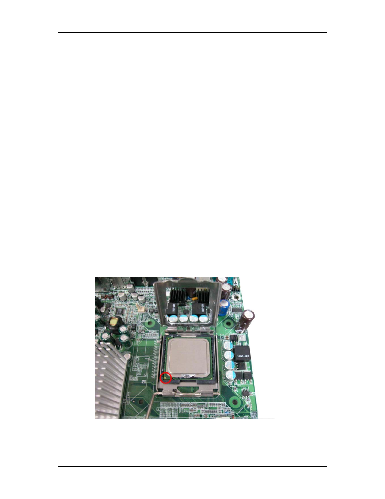
Troubleshooting
RUBY-9712VG2A User’s Manual 5-1
Chapter 5
Troubleshooting
This chapter provides a few useful tips to quickly get RUBY-9712VG2A running
with success. As basic hardware installation has been addressed in Chapter 2, this
chapter will primarily focus on system integration issues, in terms of BIOS setting,
and OS diagnostics.
5.1 Hardware Quick Installation
This chapter provides a few useful tips to quickly get RUBY-9712VG2A running
with success. As basic hardware installation has been addressed in Chapter 2, this
chapter will primarily focus on system integration issues, in terms of BIOS setting,
and OS diagnostics.
Step 1: CPU installation
This board support Intel Pentium P4 775 LGA series CPU. Be careful of CPU
orientation when you plug it into CPU socket.
(1) Pull up CPU socket cover and lever to 90-degree angel.
(2) Locate Pin 1 in the socket and look for a cut edge on CPU upper interface. Math
Pin and cut edge, then insert the CPU into the socket as Figure 5-1.
(3) Press down the CPU socket lever and finish CPU installation.
Figure 5-1
Page 70
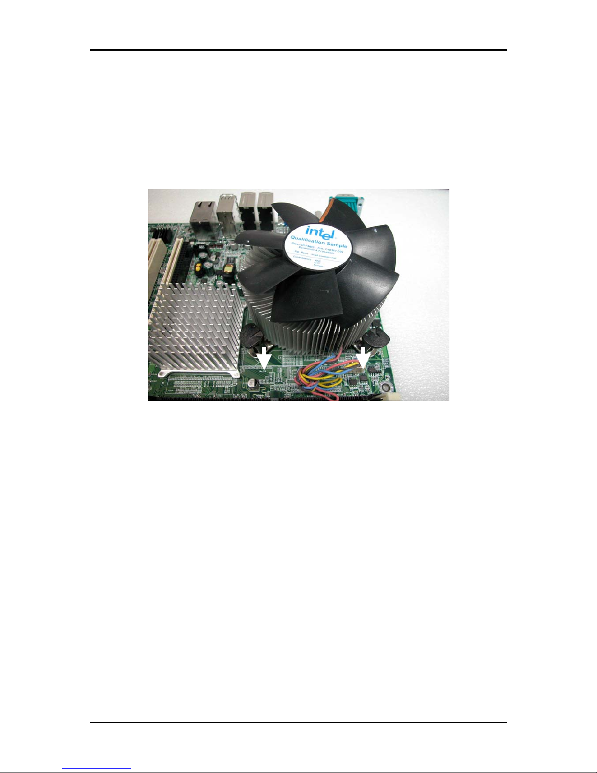
Troubleshooting
RUBY-9712VG2A User’s Manual 5-2
Step 2: CPU FAN installation
(1) Gently put the CPU FAN down on four corners correctly.
(2) Press down the four screw with force one by one, and then rotate them in a
clockwise direction.
Please make sure CPU and Fan are combined tightly, otherwise it can shutdown
automatically after running 1 minute.
Figure 5-2
Step 3: Insert DDR Memory module
(1) Make sure the DIMM module’s pin face down and match the socket’s size.
(2) Insert the module straight down to the DIMM slot with both bands and press
down firmly until the DIMM module is securely in the place.
Page 71
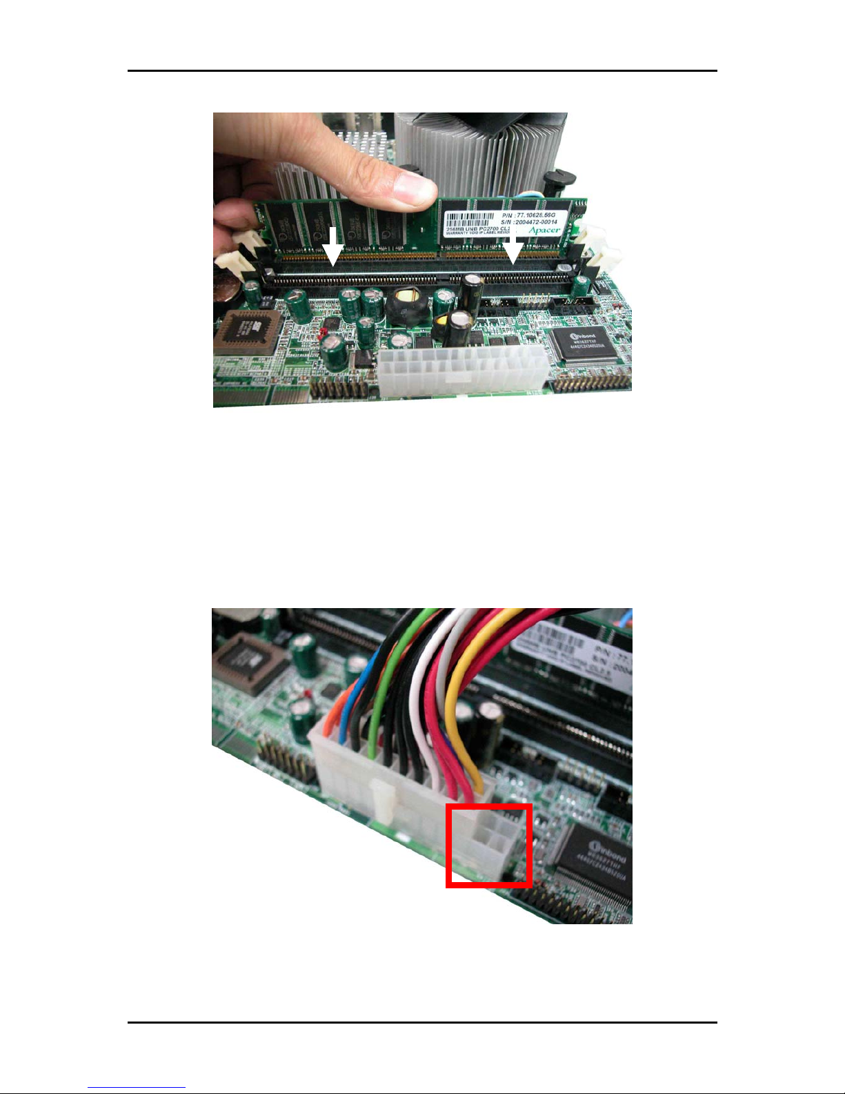
Troubleshooting
RUBY-9712VG2A User’s Manual 5-3
Figure 5-3
Step 4: Install ATX power connector
(1) Insert 20-pin ATX power connector on J27. Although it is 24-pin ATX connector,
but you still can use 20-pin ATX power supply as figure 5-4.
However, it will be better if you can adopt ATX power supply with 24-pin
connector.
Figure 5-4
Page 72
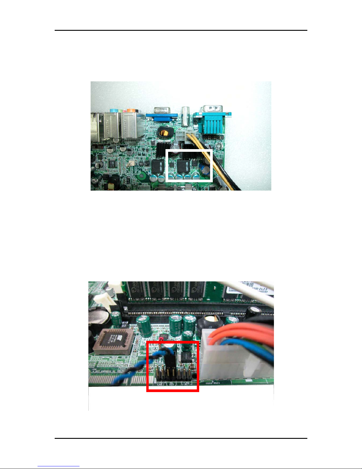
Troubleshooting
RUBY-9712VG2A User’s Manual 5-4
(2) Insert 12V 4-pin power connector on J9. Although it is 8-pin 12V power
connector, but you still can use standard 4-pin 12V power connector, if the
power supply only has 4-pin power connector.
Figure 5-5
Step 5: Boot through Power toggle switch
(1) Insert Power toggle switch on pin 6 and 8 of J30.
(2) Please make sure power is ready, and then press Power toggle switch to start the
System. Besides, you should hear short beep during booting up. Short beep
means system boot up okay. If not, please check the above steps certainty.
Figure 5-6
Page 73

Troubleshooting
RUBY-9712VG2A User’s Manual 5-5
5.2 BIOS Setting
It is assumed that users have correctly adopted modules and connected all the
device cables required before turning on power. The CPU, CPU fan, CPU fan power
cable, 184-pin DDR SDRAM, keyboard, mouse, floppy drive, IDE hard disk, printer,
VGA connector, device power cables, ATX accessories or 12V 4-pin power cable are
good examples that deserve attention. With no assurance of properly and correctly
accommodating these modules and devices, it is very possible to encounter system
failures that result in malfunction of any device.
If encounter boot failure, enter the BIOS setup program to load “Fail-Save defaults”
and change configuration accordingly.
Loading the Default Optimal Setting
When prompted with the main setup menu, please scroll down to “Load Optimal
Defaults”, press “Enter” and “Y” to load in default optimal BIOS setup. This will
force your BIOS setting back to the initial factory configuration. It is recommended
to do this so you can be sure the system is running with the BIOS setting that
Portwell has highly endorsed. As a matter of fact, users can load the default BIOS
setting any time when system appears to be unstable in boot up sequence.
Auto Detect Hard Disks
In the BIOS => Standard CMOS setup menu, pick up any one from
Primary/Secondary Master/Slave IDE ports, and press “Enter”. Setup the selected
IDE port and its access mode to “Auto”. This will force system to automatically pick
up the IDE devices that are being connected each time system boots up.
Improper Disable Operation
There are too many occasions where users disable a certain device/feature in one
application through BIOS setting. These variables may not be set back to the original
values when needed. These devices/features will certainly fail to be detected.
When the above conditions happen, it is strongly recommended to check the BIOS
settings. Make sure certain items are set as they should be. These include the floppy
drive, COM1/COM2 ports, parallel port, USB ports, external cache, on-board VGA
and Ethernet.
It is also very common that users would like to disable a certain device/port to
release IRQ resource. A few good examples are
Disable COM1 serial port to release IRQ #4
Disable COM2 serial port to release IRQ #3
Disable Parallel port to release IRQ #7
Disable PS/2 mouse to release IRQ #12 ,…, etc.
Page 74

Troubleshooting
RUBY-9712VG2A User’s Manual 5-6
A quick review of the basic IRQ mapping is given below for your reference.
IRQ# Description
IRQ #0 System Counter
IRQ #1 Keyboard
IRQ #2 Unused
IRQ #3 COM2
IRQ #4 COM1
IRQ #5 USB Controller 1.0/1.1
IRQ #5 Multimedia Controller
IRQ #5 Display Controller
IRQ #6 Floppy Controller
IRQ #7 Parallel Port
IRQ #8 Real Time Clock
IRQ #9 USB Controller 2.0 EHCI Controller
IRQ #9 USB Controller 1.0/1.1
IRQ #9 ACPI Controller
IRQ #10 USB Controller 1.0/1.1
IRQ #10 Network Controller
IRQ #11 USB Controller 1.0/1.1
IRQ #11 Network Controller
IRQ #11 SMB Controller
IRQ #12 PS/2 Mouse
IRQ #13 Unused
IRQ #14 IDE Primary Controller
IRQ #15 IDE Secondary Controller
It is then very easy to find out which IRQ resource is ready for additional peripherals.
If IRQ resource is not enough, please disable some devices listed above to release
further IRQ numbers.
Page 75
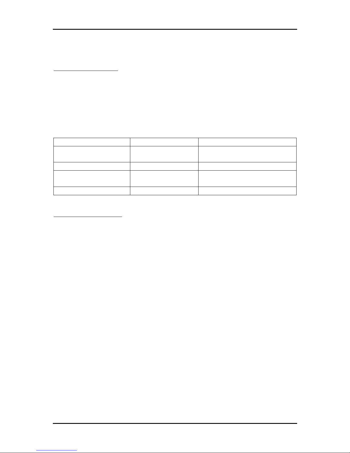
Troubleshooting
RUBY-9712VG2A User’s Manual 5-7
5.3 FAQ
Boot up failure Issues
Symptom: PUBY-9712VG2A just keeps beeping, and nothing has been shown on
the screen?
Solution: Each beep sound pattern represents different definition of error. Therefore,
refer to the table as follows. If it doesn’t still boot up normal, and you
make sure all of jumper setting, and configuration is as default, please try
to move JP3 from 1-2 to 2-3, then back to 1-2 in order to clear CMOS.
Beep sounds Meaning Action
One long beep with one
short beeps
DRAM error Change DRAM or reinstall it
One long beep constantly DRAM error Change DRAM or reinstall it
One long beep with two
short beeps
Monitor or Display
Card error
Please check Monitor connector
whether it inserts properly
Beep rapidly Power error warning Please check Power mode setting
Information & Support
Q: I am using an ATA-66 (or 100) hard drive, how can I know that ATA-66
function is started?
A: You need to use the 80-pin ATA-66 IDE flat cable to have this function ready.
During POST, you can see ATA-66 (or 100) message while hard drive is being
detected. Besides, after Microsoft series OS installation successfully, you must
install ATA-66/100 driver, then the function can be active.
Q: After changing setting of serial port from RS-232 to RS-485, why 485 function
still cannot work normally?
A: Cable must connect to same definition of pins. For example, there are only two
pins in RS-485, which are DATA – and DATA +. Its connection must be “DATA –
connects to DATA –“, and “DATA + connects to DATA +”. Otherwise, RS-485
won’t be able to transfer its data. Besides, you need to program communication of
RS-485 by yourself.
Page 76

Troubleshooting
RUBY-9712VG2A User’s Manual 5-8
Q: After installing Compact Flash, why the device on Secondary has been
missing?
A: The default setting for Compact Flash at secondary IDE channel is a salve device.
Therefore, you might want to check if your missing device is set to the same as
default setting of Compact Flash. If it is, please either set up Compact flash as
master device or your missing device as master device. The jumper to adjust slave
or master for compact flash is JP1.
Q: I am building the embedded system, but I cannot find embedded driver on
Portwell website. Where can I get them?
A: It is available on Intel website; The URL of Intel website:
http://www.intel.com/design/intarch/software/driver/index.htm. For other
devices, please visit manufacture’s website to download embedded drivers. We
will post those drivers on our website in the future.
Q: I am a customer of Portwell, where can I get new BIOS to update on IMB ?
A: You can always visit Portwell Download center to download update BIOS.
Besides, before downloading anything, please mail us to get your download
account number.
Portwell Download Center
http://www.portwell.com.tw/download.asp
To request your Account Number for Download Center, please fill out the
application form on our Web.
Note:
Please visit our technical web site at
http://www.portwell.com.tw
For additional technical information, which doesn’t covered in this manual, please email to [email protected] or contact with your sales representative, they will
be very delighted to assist you.
Page 77

Appendix A
RUBY-9712VG2A User’s Manual
System Memory Address Map
Each On-board device in the system is assigned a set of memory addresses, which
also can be identical of the device. The following table lists the system memory
address used.
Memory Area Size Device Description
0000 – 003F 1K Interrupt Area
0040 – 004F 0.3K BIOS Data Area
0050 – 006F 0.5K System Data
0070 – 04A4 16K DOS
04A5 – 0C7C 31K Program Area
0C7D – 9F3E 587K [Available]
9F3F –9FFF 3K Unused
= Conventional memory ends at 637K =
A000 – AFFF 64K VGA Graphics
B000 – B7FF 32K Unused
B800 – BFFF 32K VGA Text
C000 – CA7F 42K Video ROM
CA80 – CB00 2K Unused
CB01 – CBFE 4K High RAM
CBFF – CBFF 0.1K Unused
CC00 - D57F 38K ROM
D580 – D5FF 2K Unused
D600 – D77F 6K ROM
D780 – D949 7.2K Unused
D94A – DFFF 26K High RAM
E000 – EFFF 64K Unused
F000 – FFFF 64K System ROM
HMA 64K First 64K Extended
Page 78
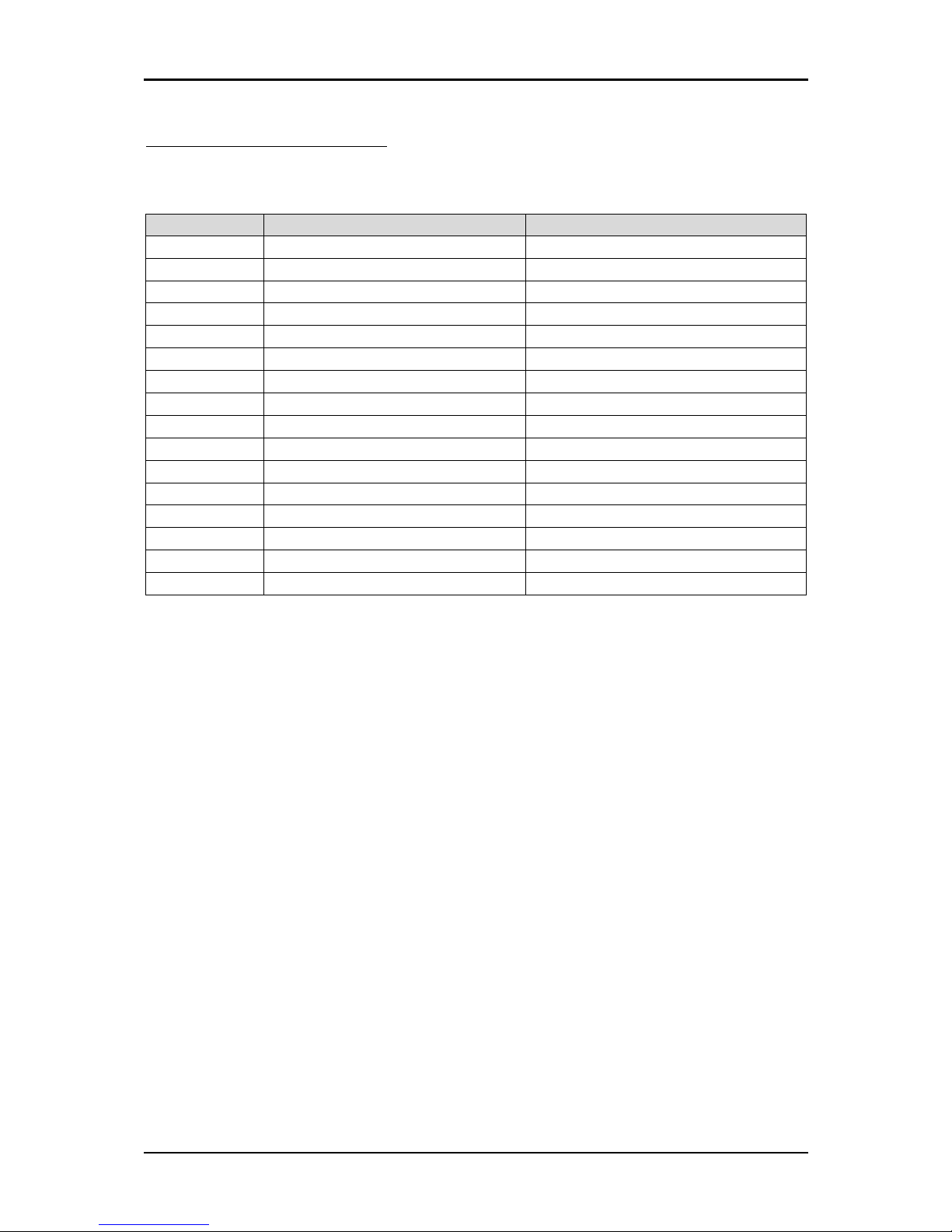
Appendix B
RUBY-9712VG2A User’s Manual
Interrupt Request Lines (IRQ)
Peripheral devices can use interrupt request lines to notify CPU for the service
required. The following table shows the IRQ used by the devices on board.
IRQ# Current Use Default Use
IRQ 0 SMARTDRV System Timer
IRQ 1 SMARTDRV Keyboard Event
IRQ 2 [Unassigned] Usable IRQ
IRQ 3 System ROM COM 2
IRQ 4 System ROM COM 1
IRQ 5 [Unassigned] Usable IRQ
IRQ 6 System ROM Diskette Event
IRQ 7 [Unassigned] Usable IRQ
IRQ 8 System ROM Real-Time Clock
IRQ 9 [Unassigned] Usable IRQ
IRQ 10 [Unassigned] Usable IRQ
IRQ 11 [Unassigned] Usable IRQ
IRQ 12 System ROM IBM Mouse Event
IRQ 13 System ROM Coprocessor Error
IRQ 14 System ROM Hard Disk Event
IRQ 15 [Unassigned] Usable IRQ
 Loading...