

Page 1

NAR-5050 Series
Communication Appliance
Users Manual
Revision: 010
P
ortwell Inc.
3F, No. 92, Sec. 1, Nei-Hu Rd., Taipei 114, Taiwan, R.O.C.
Headquarter: +886-2-2799-2020 FAX: +886-2-2799-1010
http://www.portwell.com.tw
Email: [email protected]
Page 2

NAR-5050/5070 Series User’s Manual
1
Item NO: B8980690
Table of Contents
Chapter 1 Introduction .................................................................................................................2
1.1 About This Manual.................................................................................................2
1.2 Manual Organization..............................................................................................2
1.3 Technical Support Information...............................................................................2
Chapter 2 Getting Started............................................................................................................3
2.1 Included Hardware.................................................................................................3
2.2 Before You Begin...................................................................................................3
2.3 The Chassis...........................................................................................................4
2.4 Open the Chassis..................................................................................................4
2.5 Remove and Install DIMM......................................................................................5
2.6 Remove and Install DOM.......................................................................................5
2.7 Remove and Install Battery....................................................................................6
2.8 Install HDD............................................................................................................7
2.9 Remove and Install PCI card.................................................................................9
2.10 Remove and Install PCI card.................................................................................9
2.10 Product Specifications.........................................................................................10
2.11 Hardware Configuration Setting...........................................................................11
2.12 Install a Different Processor.................................................................................14
2.13 Use a Client Computer.........................................................................................14
2.14 BIOS Setup Information.......................................................................................16
2.15 Reset to Default Information................................................................................22
2.16 WDT Information..................................................................................................25
2.17 GPIO Information.................................................................................................33
Chapter 3 Operation Guide........................................................................................................56
3.1 Brief Guide of PPAP-3710L-0200........................................................................57
3.2 System Architecture.............................................................................................57
Page 3

NAR-5050/5070 Series User’s Manual
2
Chapter 1 Introduction
1.1 About This Manual
This manual contains all required information for setting up and using the NAR-5050 series.
NAR-5050 series provides the essential platform for delivering optimal performance and
functionality in the value communications appliance market segment. This manual should
familiarize you with NAR-5050 series operations and functions. NAR-5050 series has up to
seven on-board Ethernet ports to serve communication appliances like Firewall, requiring three
Ethernet ports to connect external network (internet), demilitarized zone and internal network.
Feature of NAR-5050 series includes:
Versatile networking and I/O capabilities: 3 or 5 Ethernet ports (NAR-5050-310 and NAR-5050-510)
Two 64bit/133MHz Gigabits Ethernet (Broadcom BCM5704 (CIOB-E))
Two 64bit/66MHz Gigabits Ethernet (National Semiconductor NS83820) for NAR-5050-510 only
One 32bit/33MHz 10/100 Fast Ethernet (Intel 82551)
Up to 4GB 2.5V 200/266MHz registered DDR on 2 x 184-pin DIMM sockets, with ECC.
One on-board IDE channel (40pin or 44pin) to support up to two IDE devices
One PCI slot for ease of connectivity to the PCI bus
One PCI-X slot for ease of connectivity to the PCI-X bus
User-friendly LCD control panel
1.2 Manual Organization
This manual describes how to configure your NAR-5050 series system to meet various
operating requirements. It is divided into three chapters, with each chapter addressing the basic
concept and operation of this system.
Chapter 1: Introduction. This section describes how this document is organized. It includes brief
guidelines and overview to help find necessary information.
Chapter 2: Hardware Configuration Setting and Installation. This chapter demonstrated the
hardware assembly procedure, including detailed information. It shows the definitions
and locations of Jumpers and Connectors that can be used to configure the system.
Descriptions on how to properly mount the CPU and main memory are also included to
help perform a safe installation. This chapter will provide detailed instruction on how to
set up NAR-5050 series.
Chapter 3: Operation Information. This section provides illustrations and information on the
system architecture and how to optimize its performance.
Any updates to this manual, technical clarification and answers to frequently asked questions
would be posted on the web site: http://isc.portwell.com.tw
1.3 Technical Support Information
Users may find helpful tips or related information on Portwell's web site: http://www.portwell.com.tw.
A direct contact to Portwell's technical person is also available. For further support, users may
also contact Portwell’s headquarter in Taipei or local distributors.
Page 4

NAR-5050/5070 Series User’s Manual
3
Taipei Office Phone Number: +886-2-27992020
Chapter 2 Getting Started
This section describes how the hardware installation and system settings should be done.
2.1 Included Hardware
The following hardware is included in package:
PPAP-3710L-0200 Communication Appliance System Board
One null serial port cable
2.2 Before You Begin
To prevent damage to any system board, it is important to handle it with care. The following
measures are generally sufficient to protect your equipment from static electricity discharge:
When handling the board, use a grounded wrist strap designed for static discharge elimination
and touch a grounded metal object before removing the board from the antistatic bag. Handle
the board by its edges only; do not touch its components, peripheral chips, memory modules or
gold contacts.
When handling processor chips or memory modules, avoid touching their pins or gold edge
fingers. Restore the communications appliance system board and peripherals back into the
antistatic bag when they are not in use or not installed in the chassis.
Some circuitry on the system board can continue operating even though the power is switched
off. Under no circumstances should the Lithium battery cell used to power the real-time clock be
allowed to be shorted. The battery cell may heat up under these conditions and present a burn
hazard.
WARNING!
1. "CAUTION: DANGER OF EXPLOSION IF BATTERY IS INCORRECTLY REPLACED. REPLACE
ONLY WITH SAME OR EQUIVALENT TYPE RECOMMENDED BY THE MANUFACTURER.
DISCARD USED BATTERIES ACCORDING TO THE MANUFACTURER’S INSTRUCTIONS"
2. This guide is for technically qualified personnel who have experience installing and
configuring system boards. Disconnect the system board power supply from its power
source before you connect/disconnect cables or install/remove any system board
components. Failure to do this can result in personnel injury or equipment damage.
3. Avoid short-circuiting the lithium battery; this can cause it to superheat and cause burns if
touched.
4. Do not operate the processor without a thermal solution. Damage to the processor can occur
in seconds.
5. Do not block air vents. Minimum 1/2-inch clearance required.
Page 5
NAR-5050/5070 Series User’s Manual
4
2.3 The Chassis
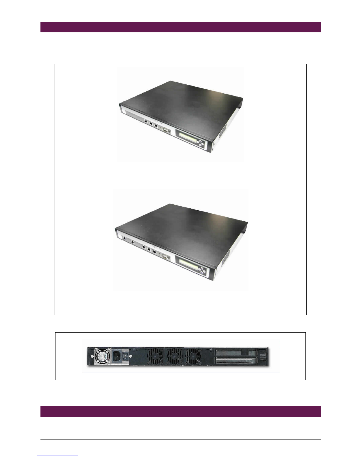
The system is integrated in a customized 1U chassis (Fig. 2-1, Fig. 2-2). On the front panel you
will find a 4-push-button LCD module (EZIO), three or five LAN ports and a COM port.
NAR-5050-310
NAR-5050-510
Fig. 2-1 Front view of the chassis
Fig. 2-2 Rear view of the chassis
2.4 Open the Chassis
Page 6
NAR-5050/5070 Series User’s Manual
5
1.
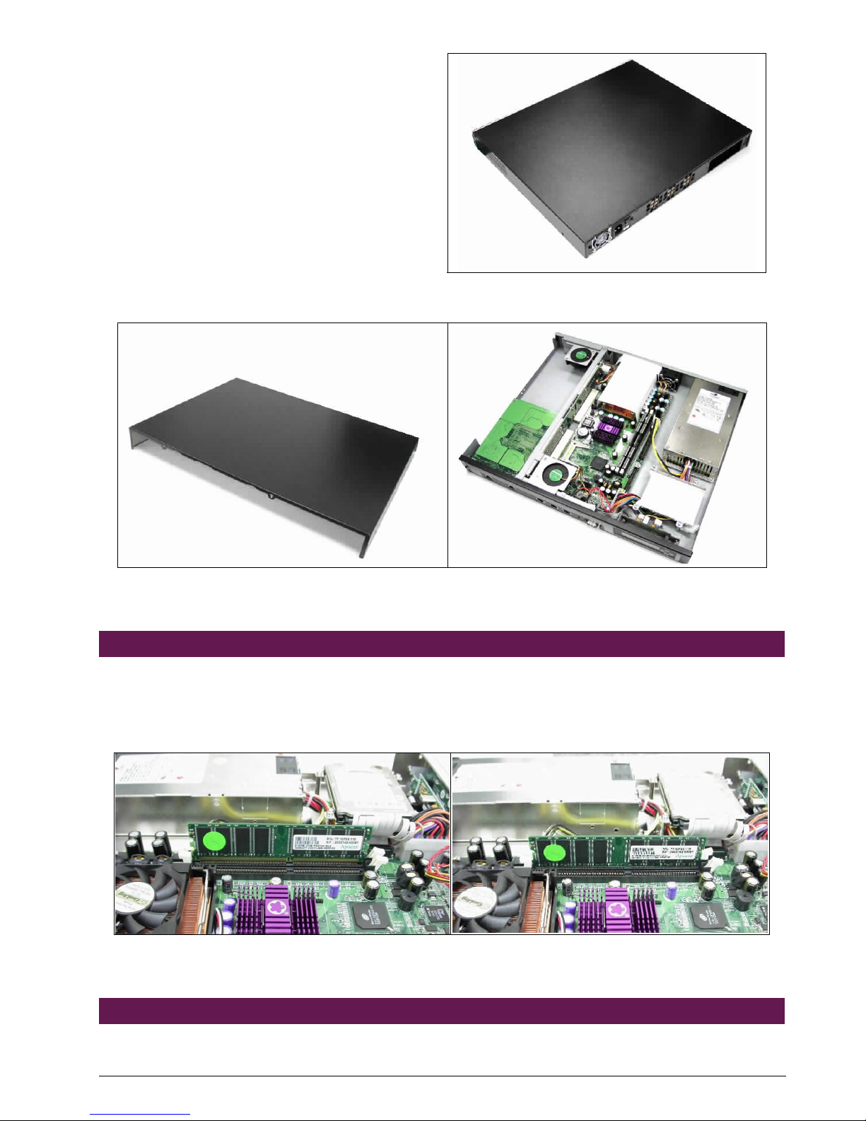
Loosen the six screws of the chassis,
two on each side and the rest two on the
back
, to remove the top lead
(Fig. 2-3).
Fig. 2-3 Take off screws
2. The top lead (Fig. 2-4) can be removed from the base stand (Fig. 2-5).
Fig. 2-4 The top lead Fig. 2-5 The base stand
2.5 Remove and Install DIMM
Follow these steps to upgrade RAM module:
1. Install the system memory by pulling the socket’s arm and pressing it into the slot gently.
(Fig. 2-6, 2-7)
Fig. 2-6 Eject a DIMM module Fig. 2-7 Install DIMM
2.6 Remove and Install Compact Flash Card
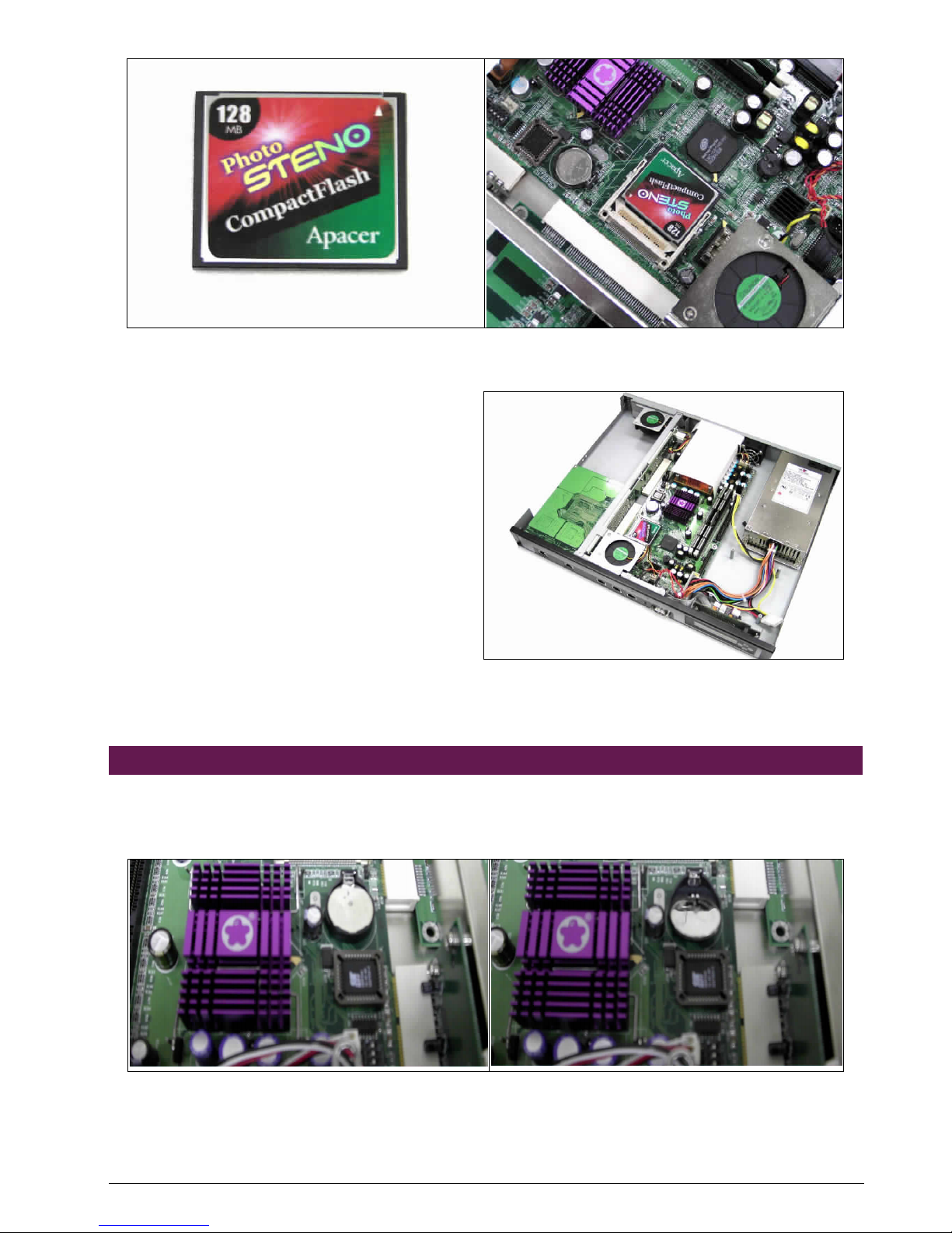
1. Insert the Compact Flash Card (Fig. 2-8) into the CF interface (Fig. 2-9).
Page 7
NAR-5050/5070 Series User’s Manual
6
Fig. 2-8 Compact Flash Card Fig. 2-9 Insert Compact Flash Card into the CF
interface
2. The completed installation of Compact
Flash Card is shown as Fig. 2-10.
Fig. 2-10 Completion of Compact Flash Card
connection
2.7 Remove and Install Battery
1. Press the metal clip back to eject the button battery (Fig. 2-11).
2. Replace it with a new one by pressing the battery with fingertip to restore the battery (Fig. 2-12).
Fig. 2-11 Eject the battery Fig. 2-12 Restore the battery
Page 8
NAR-5050/5070 Series User’s Manual
7
2.8 Install HDD
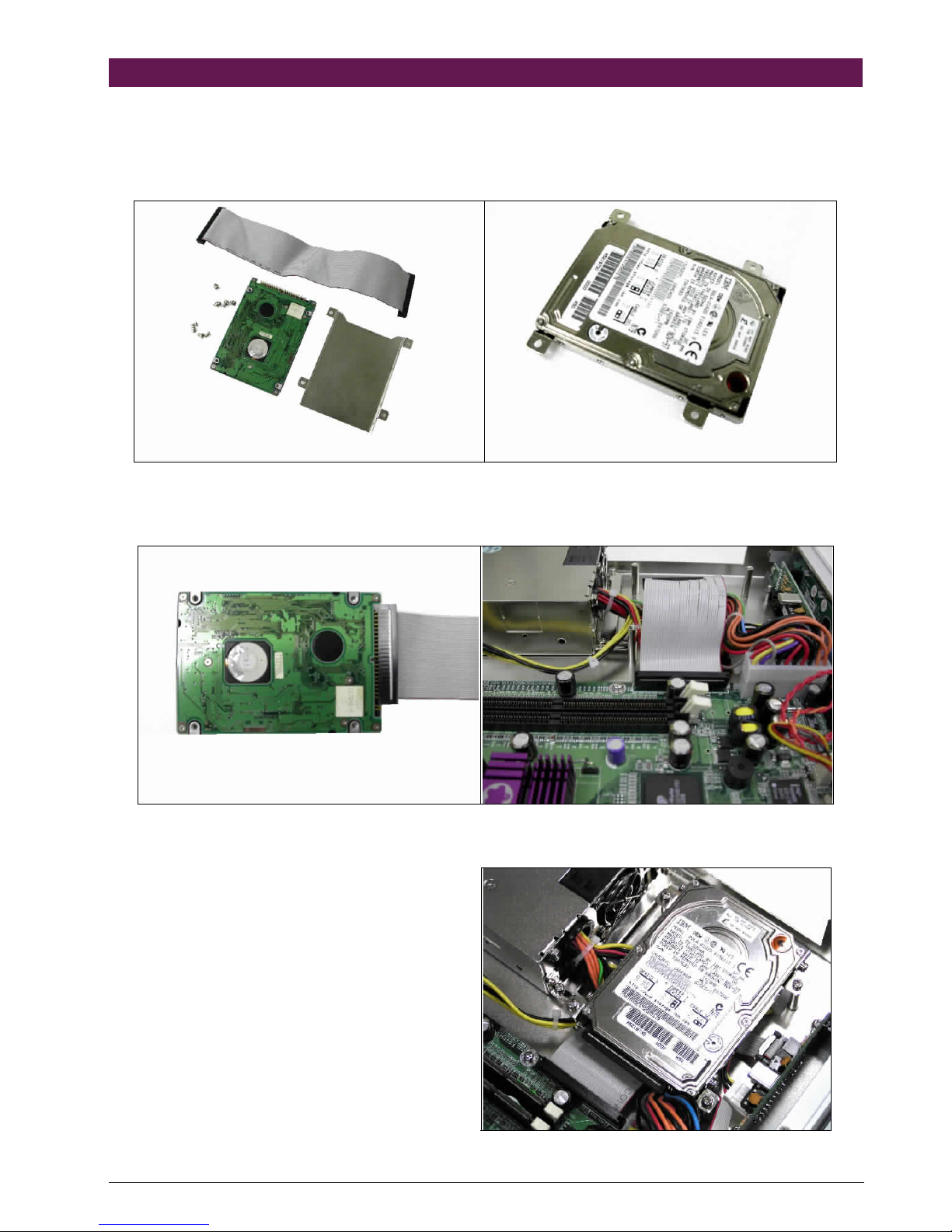
The system has an internal drive bay for one 2.5" hard disk drive. If the HDD is not pre-installed,
you can install it by yourself. Follow the steps below to install the HDD:
1. Fasten the four screws to lock HDD and bracket together (Fig. 2-13a, 2-13b).
Fig. 2-13a A 2.5” HDD and the HDD bracket Fig. 2-13b Fix HDD to the bracket
2. Connect the IDE cable to HDD (Fig. 2-14).
3. Connect IDE cable to PPAP-3710L-0200 (Fig. 2-15).
Fig. 2-14 Connect IDE cable to HDD Fig. 2-15 Connect IDE cable to PPAP-3710L-
0200
4. Fix all four screws back (Fig. 2-16).
Fig. 2-16 Drive all four screws back
Page 9
NAR-5050/5070 Series User’s Manual
8
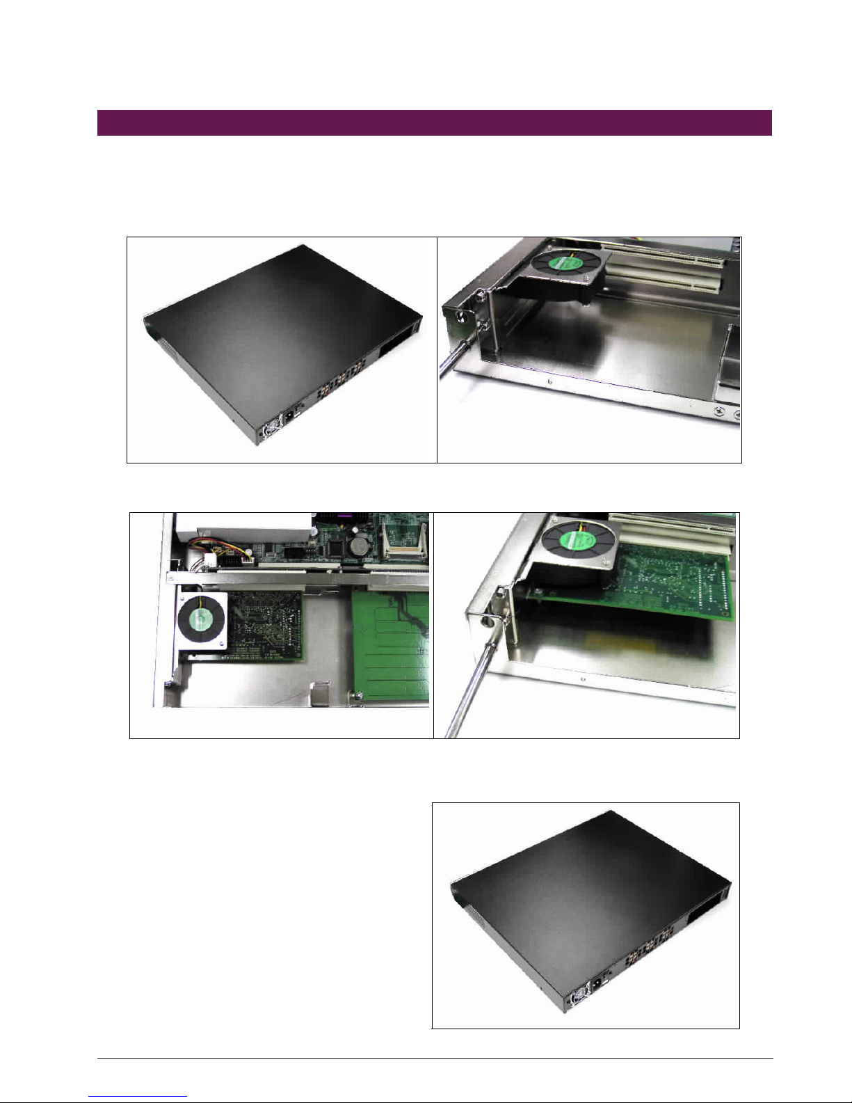
2.9 Remove and Install PCI card
One PCI slot is available to NAR-5050 series. Follow the steps below for installation:
1. Loosen the screws (on the top lead) and remove the top lead (Fig. 2-17).
2. Remove the screw on the side (Fig. 2-18).
Fig. 2-17 The top lead Fig.2-18 Remove the screw on the side
3. Push the PCI add-on card into the PCI slot (Fig. 2-19).
Fig.2-19 Push the PCI add-on card into the PCI
slot
Fig.2-20 Fasten the screw into the side
4. Fasten the screw from the side (Fig. 2-20).
5. Drive the screws on the top lead
(Fig. 2-21).
Fig. 2
-21 Drive
the screws
back to
lock the top
Page 10
NAR-5050/5070 Series User’s Manual
9
lead
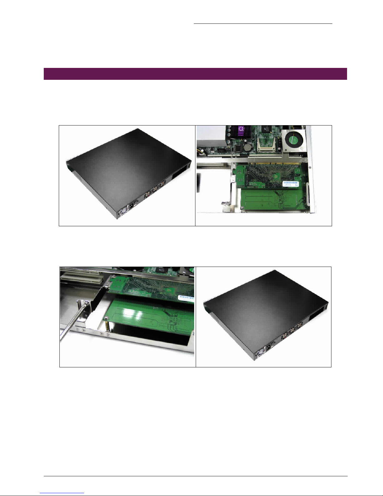
2.10 Remove and Install PCI-X card
One PCI-X slot is available to NAR-5050 series. Follow the steps below for installation:
6. Loosen the screws (on the top lead) and remove the top lead (Fig. 2-22).
7. Push the PCI-X add-on card into the PCI-X slot (Fig. 2-23).
Fig. 2-22 The top lead Fig.2-23 Push the PCI-X add-on card into the
PCI-X slot
8. Fasten the screw from the side (Fig. 2-24).
9. Drive the screws back to lock the top lead (Fig. 2-25).
Fig.2-24 Fasten the screw into the side Fig.2-25 Drive the screws back to lock the
top lead
Page 11

NAR-5050/5070 Series User’s Manual
10
2.10 Product Specifications
Model:
NAR-5050 series
Main Processor:
Intel® socket 478 Pentium® 4 processors
(400 or 533MHz system bus)
BIOS:
Award system BIOS with 512KB flash ROM to support DMI,
PnP, APM function
Main Memory:
Two 200/266MHz registered DDR on 184-pin DIMM socket
supports up to 4GB of 2.5V DIMM, with ECC.
L2 Cache Memory:
256KB/512KB PBSRAM built in (Celeron/Pentium 4) CPU
module
Chipset:
North Bridge: Server Works CMIC-SL
South Bridge: Server Works CSB5
I/O Bridge: CIOB-E
PCI IDE Interface:
One 2.5” hard disk bay for DMA/33/66/100 IDE hard disk
Serial Ports:
Support two high-speed 16550C compatible UARTs with 16-byte
T/R FIFOs
(Optional) Support LCD/Key pad module (Portwell proprietary)
USB Interface:
Support two USB1.0 ports for high speed I/O peripheral devices
Auxiliary I/O Interfaces:
System reset switch, power okay LED and HDD LED interface
Power Input:
Support one AC input jack (power requirement: 110V ~ 220V)
PCI Slot:
One PCI slot for add-on PCI card
PCI-X Slot:
One PCI-X slot for add-on PCI-X card
On-board Ethernet:
One Intel® 82551 10/100 Fast Ethernet controllers with RJ-45
interface for NAR-5050-310 and NAR-5050-510
One Intel® 82540EM 10/100/1000 Gigabit Fast Ethernet
controllers and two NS 83820 10/100/1000 Gigabit Fast Ethernet
with RJ-45 interface for NAR-5050-510
Two Broadcom® BCM5704 10/100/1000 Gigabit Fast Ethernet
controllers with RJ-45 interface
Hardware Monitor:
Support on-board hardware monitor for
CPU fan x 1
Chassis fan x 4
System voltages: Vcore, 3.3V, +5V and +12V
Power Good:
On-board power good interval: 100ms ~ 500ms
Environmental
Requirements:
Operating Temperature: 5°C ~ 40°C
Storage Temperature: 5°C ~ 70°C
Relative Humidity: 5% ∼ 95%, non-condensing
Dimension:
16.89"(D) x 14.1"(W) x 1.73“(H)
Page 12
NAR-5050/5070 Series User’s Manual
11
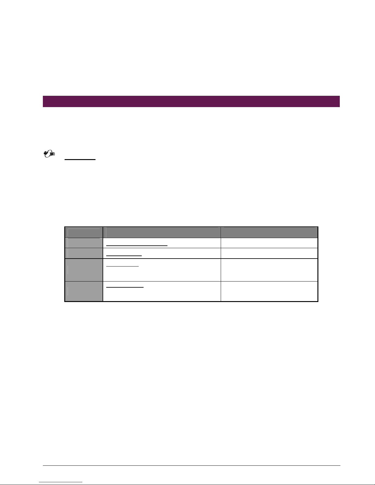
2.11 Hardware Configuration Setting
This section gives the definitions and shows the positions of jumpers, headers and connectors.
All of the configuration jumpers on PPAP-3710L-0200 are in the proper position. The default
settings set by factory are marked with a star ( ★ ).
Jumpers
In general, jumpers on PPAP-3710L-0200 system board are used to select options for
certain features. Some of the jumpers are configurable for system enhancement. The
others are for testing purpose only and should not be altered. To select any option, cover
the jumper cap over (Short) or remove (NC) it from the jumper pins according to the
following instructions. Here NC stands for “Not Connected”.
Jumper Table
Jumper Function Default Setting
JP1 1-2
Reset to Default function: NC: Normal
JP1 3-4
System Reset:
NC: Normal
JP3
CMOS Clear:
1-2: CMOS normal
2-3: CMOS clear
CMOS normal
JP4
PCI bus detect:
Open: PCI-X or PCI auto detect
Short: PCI 32 or PCI 64 only
Open: PCI-X or PCI auto detect
Page 13
NAR-5050/5070 Series User’s Manual
12
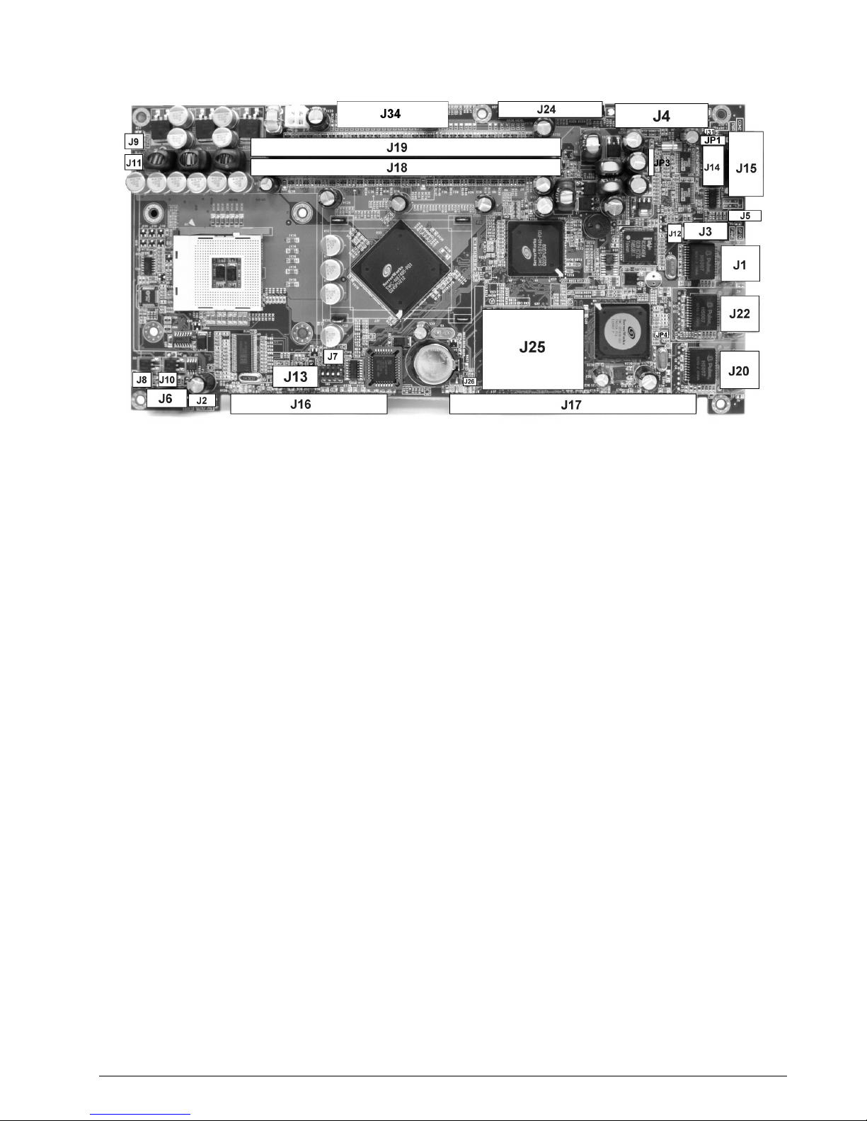
Figure 2-22 PPAP-3710L-0200 Jumper Table
Page 14

NAR-5050/5070 Series User’s Manual
13
Connector
Connector
Function
J1
LAN#1 Gbit (BUS#0,DEVSEL#2)
J2
AUX 5V OUT
J3
GPIO
J4
ATX POWER CONNECTOR
J5
POWER(GREEN) & IDE(ORANGE) LED
J6
USB
J7
CPU FAN
J8
SYSTEM FAN#1
J9
SYSTEM FAN#2
J10
SYSTEM FAN#3
J11
SYSTEM FAN#4
J12
FORNT PANEL FAN
J13
PS2 KEYBOARD/MOUSE
J14
COM2
J15
COM1
J16
PCI32
J17
PCI-X
J18
DIMM#1
J19
DIMM#2
J20
LAN#2
J22
LAN#3
J24
IDE CNANNEL0 (44pin)
J25
IDE CHANNEL1 CF CARD
J26
CHASSIS INTRUSION
J31
POWER ON
J34
IDE CNANNEL0 (40pin)
Page 15

NAR-5050/5070 Series User’s Manual
14
2.12 Install a Different Processor
Install CPU
1. Lift the handling lever of CPU socket outwards and upwards to the other end.
2. Align the processor pins with holes on the socket. Make sure that the notched corner or dot
mark (pin 1) of the CPU corresponds to the socket's bevel end. Then press the CPU gently
until it fits into place. If this operation is not easy or smooth, don't do it forcibly. You need to
check and rebuild the CPU pin uniformly.
3. Push down the lever to lock processor chip into the socket.
4. Follow the installation guide of cooling fan or heat sink to mount it on CPU surface and lock it
on the socket 478.
5. Be sure to follow particular CPU speed and voltage type to adjust the jumper settings properly
for all boards.
Remove CPU
1. Unlock the cooling fan first.
2. Lift the lever of CPU socket outwards and upwards to the other end.
3. Carefully lift up the existing CPU to remove it from the socket.
4. Follow the steps of CPU installation to change to another one or place handling bar to close
the opened socket.
Configure Processor Speed
The system was designed to self-detect its CPU speed. So it does not require any system
adjustment.
2.13 Use a Client Computer
Connection Using Hyper Terminal
If users use a headless NAR-5050 series, which has no mouse/keyboard and VGA output
connected to it, the console may be used to communicate with NAR-5050 series.
To access NAR-5050 series via the console, Hyper Terminal is one of many choices.
Follow the steps below for the setup:
Note: Terminal software may need to update for correct console output.
1. Execute HyperTerminal under C:\Program Files\Accessories\HyperTerminal
Page 16
NAR-5050/5070 Series User’s Manual
15
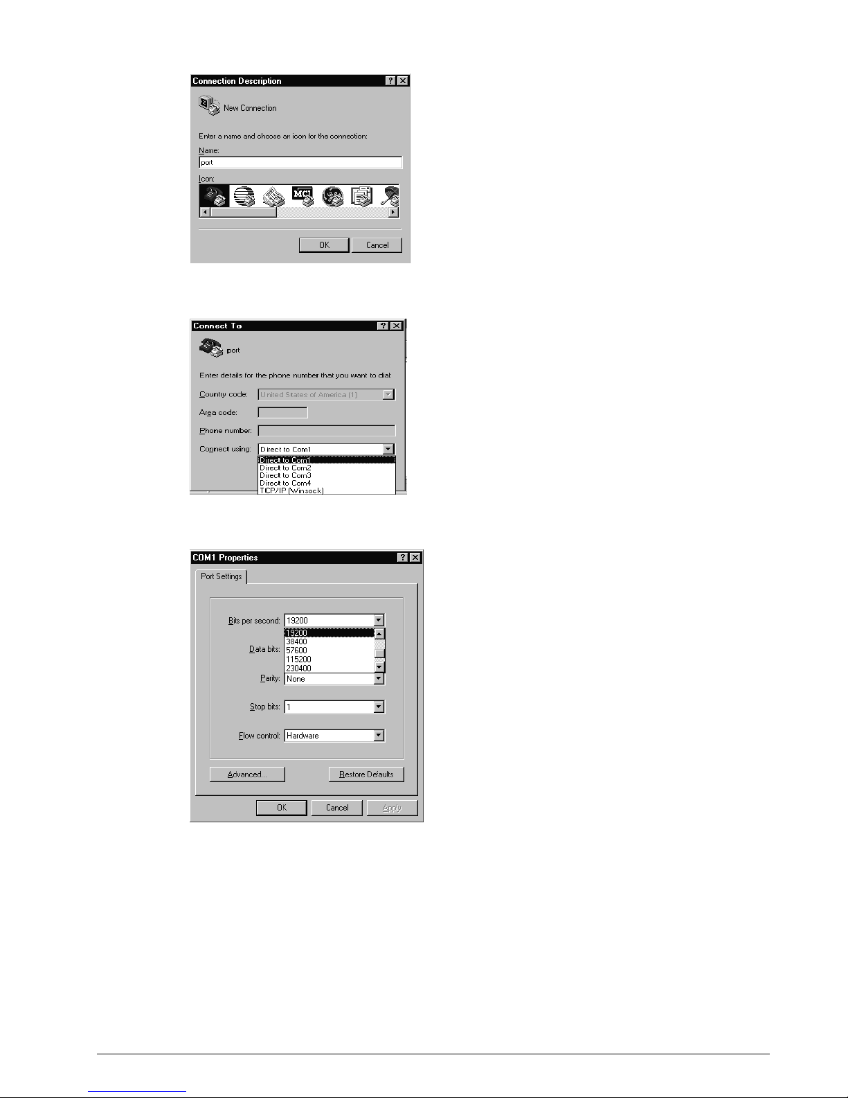
2. Enter a name to create new dial
3. For the connection settings, make it Direct to Com1.
4. Please make the port settings to Baud rate 19200, Parity None, Data bits 8, Stop bits 1
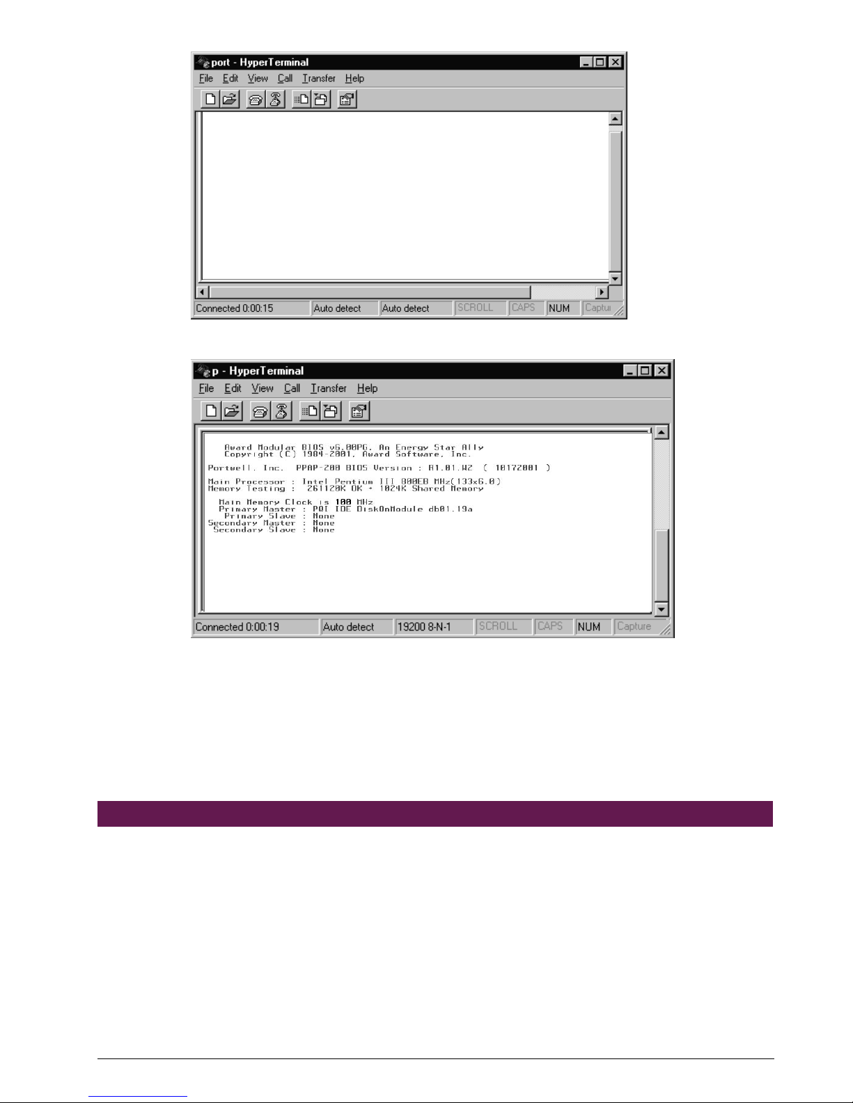
5. Turn on the power of NAR-5050 series, after following screen was shown:
Page 17
NAR-5050/5070 Series User’s Manual
16
6. You can then see the boot up information of NAR-5050 series.
7. When message “Hit <DEL> if you want to run Setup” appear during POST, after turning on or
rebooting the computer, press <Tab> key immediately to enter BIOS setup program.
This is the end of this section. If the terminal did not port correctly, please check the previous
steps.
2.14 BIOS Setup Information
NAR-5050 series is equipped with the Award BIOS within Flash ROM. The BIOS has a built-in
setup program that allows users to modify the basic system configuration easily. This type of
information is stored in CMOS RAM so that it still retains during power-off periods. When system is
turned on, NAR-5050 series communicates with peripheral devices and checks its hardware
resources against the configuration information stored in the CMOS memory. Whenever an error is
detected, or the CMOS parameters need to be initially defined, the diagnostic program will prompt
the user to enter the Setup program. Some errors are significant enough to abort the start-up.
Page 18
NAR-5050/5070 Series User’s Manual
17
Entering Setup
When message “Hit <DEL> if you want to run Setup” appear during POST, after turning
on or rebooting the computer, press <Del> key immediately to enter BIOS setup
program.
To enter Setup but fail to respond before the message disappears, please restart the
system either by first turning it off and followed by turning it on (COLD START) or simply
press the "RESET" button. “WARM START” (press <Ctrl>, <Alt>, and <Delete> keys
simultaneously) will do as well.
When no setting is stored in BIOS or the setting is missing, a message “Press <F1> to
run Setup” will appear. Then press <F1> to run Setup or resume HIFLEX BIOS Setup.
User can use the keyboard to choose among options or modify the system parameters to
match the options with your system. The table shown on next page will navigate through
all of keystroke functions in BIOS Setup.
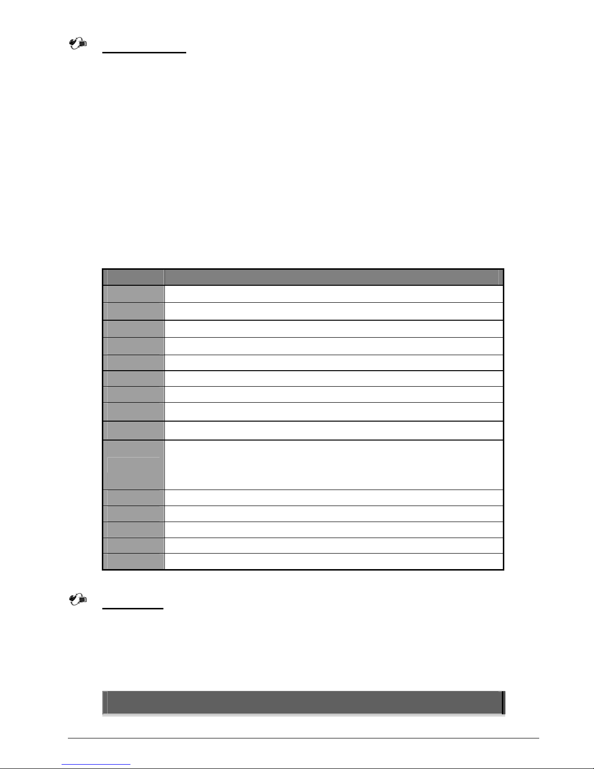
Keys to navigate within Setup menu
Key Function
Up (↑) Move to the previous item
Down (↓)
Move to the next item
Left (→) Move to the item on the left (menu bar)
Right (←) Move to the item on the right (menu bar)
Enter
Enter the item you desired
PgUp
Increase the numeric value or make changes
PgDn
Decrease the numeric value or make changes
┼ Increase the numeric value or make changes
─
Decrease the numeric value or make changes
Esc
Main Menu:
Quit and not save changes into CMOS
Status Page Setup Menu and Option Page Setup Menu:
Exit current page and return to Main Menu
F1
General help on SETUP navigation keys
F5
Load previous values from CMOS
F6
Load the fail-safe defaults from BIOS default table
F7
Load the optimized defaults
F10
Save all the CMOS changes and exit
Main Menu
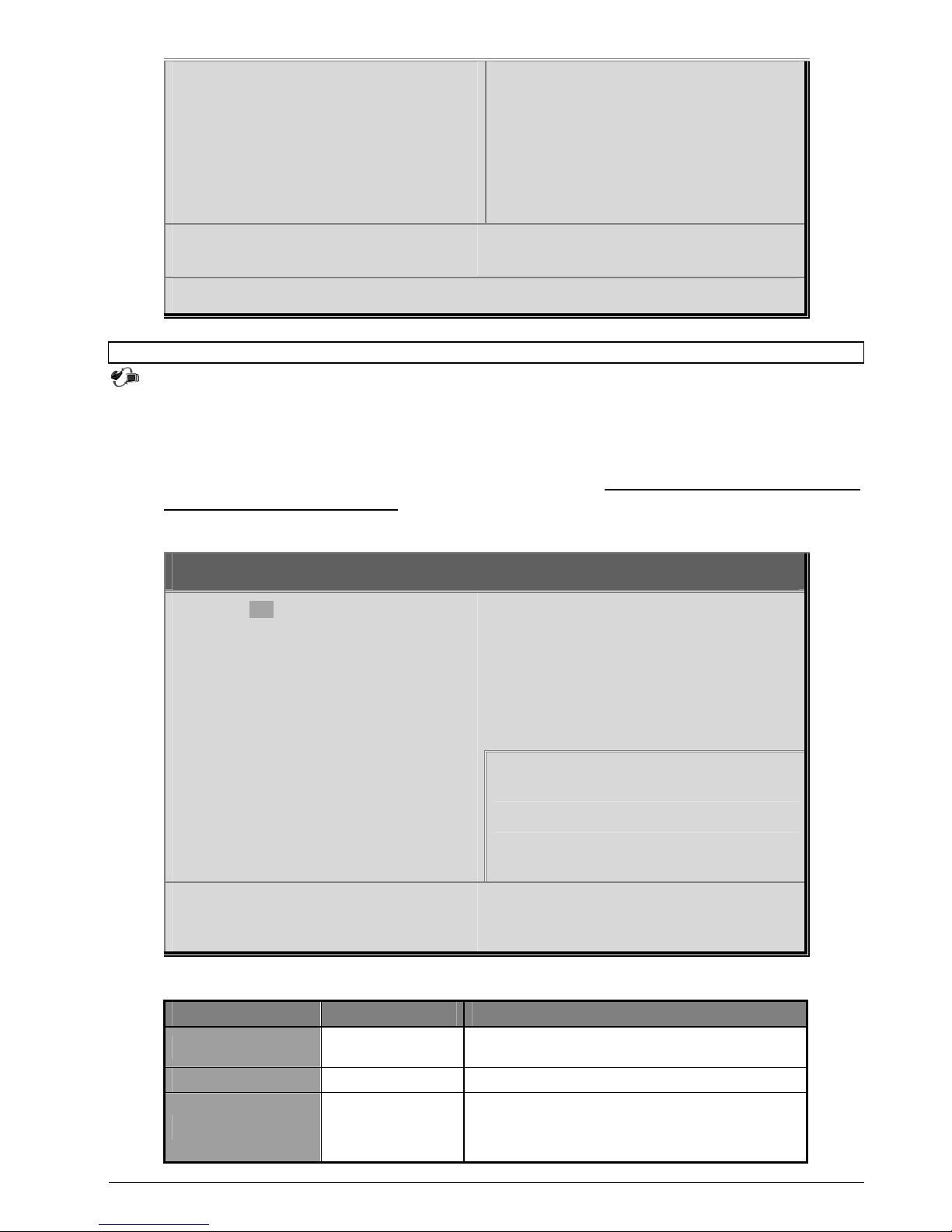
Within NAR-5050 series Award BIOS CMOS Setup utility, user should start with the Main Menu.
The Main Menu allows to select from eleven setup functions and two exit choices. Use arrow
keys to switch among items and press <Enter> to accept or bring up the sub-menu.
Phoenix – Award BIOS CMOS Setup Utility
CMOS Setup Utility
Page 19
NAR-5050/5070 Series User’s Manual
18
Standard CMOS Features
Advanced BIOS Features
Advanced Chipset Features
Integrated Peripherals
Power Management Setup
PnP/PCI Configurations
PC Health Status
Frequency /Voltage Control
Load Fail/Safe Defaults
Load Optimized Defaults
Set Supervisor Password
Set User Password
Save & Exit Setup
Exit Without Saving
ESC: Quit
F10: Save & Exit Setup
: Select Item
(Shift) F2: Change Color
Time, Date, Hard Disk Type ...
NOTE: It is strongly recommended to reload the optimized default setting if CMOS is lost or BIOS is updated.
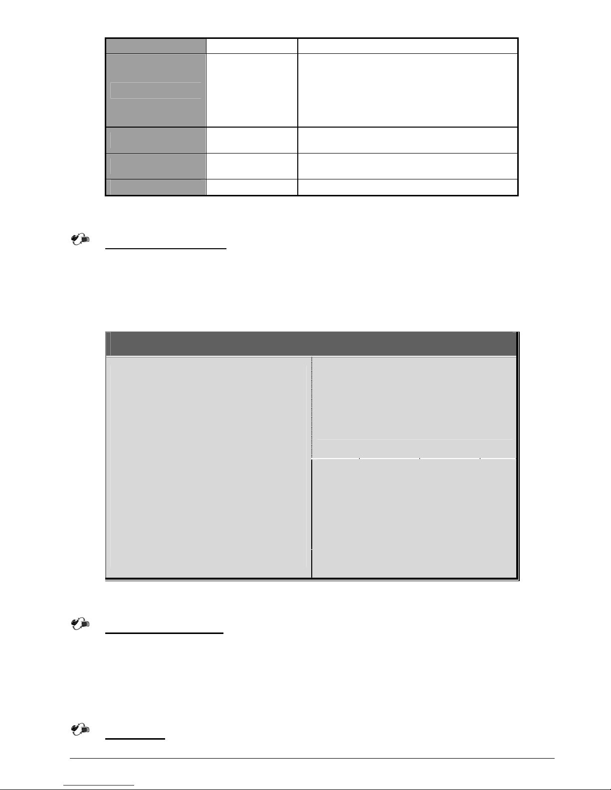
Standard CMOS Setup Menu
This setup page includes all the items within standard compatible BIOS. Use the arrow
keys to highlight the item and then use the <PgUp>/<PgDn> or <+>/<-> keys to select the
value or number you want in each item and press <Enter> to certify it.
Follow command keys in CMOS Setup table to change Date, Time, Drive type and Boot
Sector Virus Protection Status.
Screen Shot: Phoenix – Award BIOS CMOS Setup Utility
Standard CMOS Setup Utility
Date: Wed, Jan 17 2001
Time: 16:51:13
IDE Primary Master [None]
IDE Primary Slave [None]
IDE Secondary Master [None]
IDE Secondary Slave [None]
Video: EGA/VGA
Halt On: All, but Keyboard
Base Memory: 640K
Extended Memory: 64512K
Total Memory: 65536K
ESC: Quit
F1: Help
PU/PD/+/-: Modify
: Select Item
(Shift) F2: Change Color
Menu Selections
Item Options Description
Date
mm:dd:yy
Set the system date. Note that the 'Day'
automatically changes when you set the date
Time
hh:mm:ss Set the system time
Video
EGA/VGA
CGA
40CGA
Select the default video device
Page 20
NAR-5050/5070 Series User’s Manual
19
80MONO
Halt On
All Errors
No Errors
All, but Keyboard
All, but Diskette
All, but Disk/Key
Select the situation in which you want the BIOS
to stop the POST process and notify you
Base Memory
N/A
Display the amount of conventional memory
detected during boot up
Extended Memory
N/A
Display the amount of extended memory
detected during boot-up
Total Memory
N/A Display the total memory available in the system
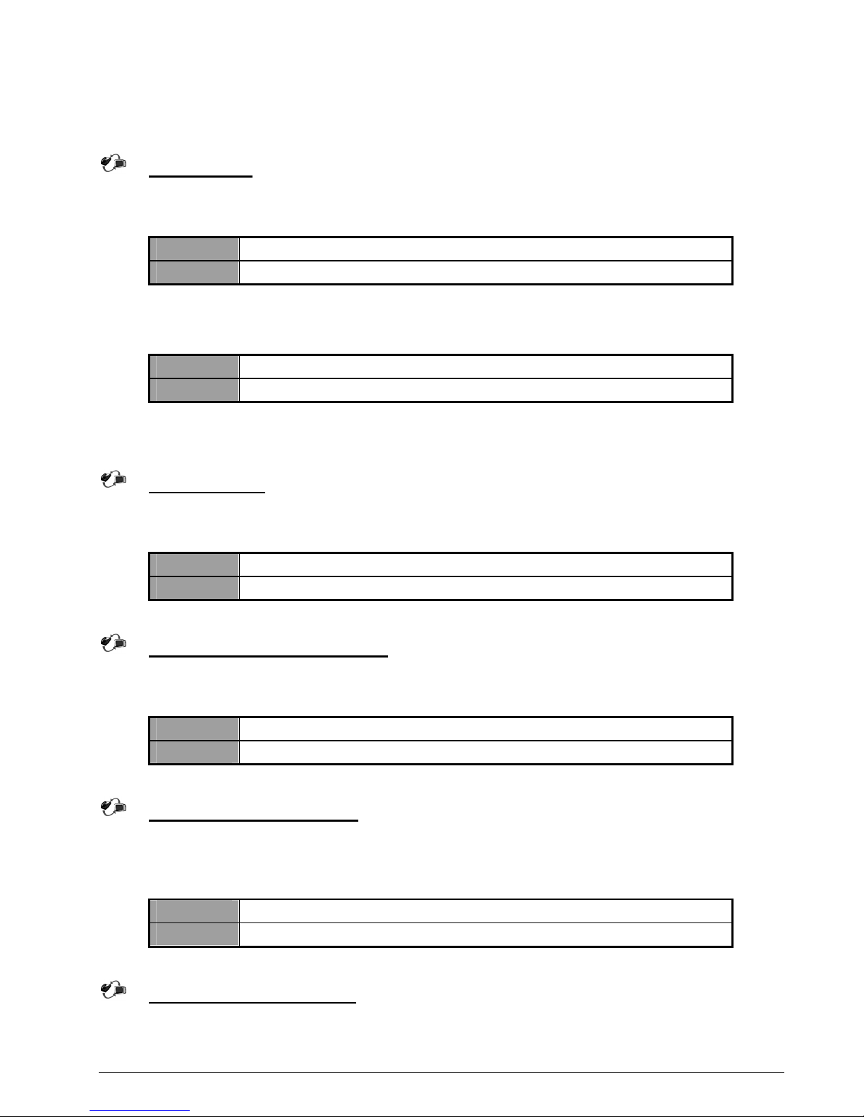
BIOS Features Setup
This section allows you to configure your system for basic operation. You are able to
select the system’s default speed, boot-up sequence, keyboard operation, shadowing and
security.
Screen Shot: Phoenix – Award BIOS CMOS Setup Utility
Advanced BIOS Features
Console Redirection: Disabled
Agent connect via: NULL
Agent wait time (min.): 1
Agent after boot: Disabled
Boot Seq & Floppy Setup [Press Enter]
Console Redirection [Press Enter]
Cache Setup [Press Enter]
Virus Warning [Disable]
Hyper-Threading Technology[Enabled]
Quick Power On Self Test: [Enabled]
Boot Up NumLock Status On
Typematic Rate Setting Disabled
Typematic Rate (Chars/Sec) 6
Typematic Delay (Msec) 250
Security Option [Setup]
OS Select for DRAM > 64MB [Non-OS2]
Small Logo(EPA) Show [Disable]
ESC: Quit
: Select Item
F1: Help
(Shift) F2: Color
F5: Old Values
F6: Load BIOS Default
F7: Load Setup Default
PU/PD/+/-: Modify
Console Redirection
Set the UNIX Console redirect to the terminal from COM1.
The choice: Enabled/Disabled.
Baud Rate
Page 21
NAR-5050/5070 Series User’s Manual
20
Set the RS-232 baud rate speed.
The choice: 9600, 19200, 38400, 57600 and 115200.
Cache Setup
CPU L1 & L2 Cache ( Enabled or Disabled CPU L1 and L2 cache )
Enabled
Enable cache
Disabled
Disable cache
CPU L2 Cache ECC Checking ( Enabled or Disabled CPU L2 cache ECC checking )
Enabled
Enable checking
Disabled
Disable checking
Virus Warning
Allows you to choose the VIRUS warning feature for IDE Hard Disk boot sector protection.
Enabled
Enable VIRUS warning
Disabled
Disabled VIRUS warning
Hyper-Threading Technology
For WindowsXP and Linux 2.4.x ( OS optimized for Hyper Threading Technology )
Enabled
Enable Hyper Threading Technology
Disabled
Disabled Hyper Threading Technology
Quick Power On Self Test
This category speeds up Power On Self Test (POST) after you power up the computer. If
it is set to Enable, BIOS will shorten or skip some check items during POST.
Enabled
Enable quick POST
Disabled
Normal POST
Boot Up NumLock Status
Select power on state for NumLock.
Page 22
NAR-5050/5070 Series User’s Manual
21
The choice: Enabled/Disabled.
Typematic Rate Setting
Keystrokes repeat at a rate determined by the keyboard controller. When enabled, the
typematic rate and typematic delay can be selected.
The choice: Enabled/Disabled.
Typematic Rate (Chars/Sec)
Set the how many number of times a second to repeat a keystroke when you hold the key
down.
The choice: 6, 8, 10, 12, 15, 20, 24 and 30.
Typematic Delay (Msec)
Set the delay time after the key is held down before it begins to repeat the keystroke.
The choice: 250, 500, 750 and 1000.
Security Option
Select whether the password is required every time the system boots or only when
entering setup.
System
The system will not boot and access to Setup will be denied if the correct
password is not entered at the prompt.
Setup
The system will boot and access to Setup will be denied if the correct password
is not entered at the prompt.
OS Select for DRAM > 64MB
Select the operating system that is running with more than 64MB of RAM on the system.
The choice: Non-OS2, OS2.
Page 23

NAR-5050/5070 Series User’s Manual
22
2.15 Reset to Default Information
This programming guide is for PPAP-3710L-0200 Reset to Default (RST2DFT)
feature.
Pin51 of NS PC87417, GPIO45, is defined as RST2DFT status pin that can be read
out to indicate RST2DFT flag.
The RST2DFT flag is defined as following:
(1) "1" : Normal State
Two events will set this flag to "1".
One is "PCI Reset Asserted", the other is "Read SET_RST2DFT I/O port".
(2) "0" : Load Default State.
The trigger event is by shorting JP1 pin1 and pin2 in a short time and then
released, i.e. making an active pulse/edge.
(JP1 "pin1 and pin2" pin header can be connected to a push button. When
the button has been pressed and released, a trigger event will clear
RST2DFT flag to "0" and System will enter to the Load Default state.
System can start the Load Default process due to RST2DFT flag is "0".)
RST2DFT flag can be polled and read its status periodically.
This flag can be set to "1" by reading the SET_RST2DFT I/O port and back to the
normal state.
SET_RST2DFT I/O port Address is "CDEFh" by BIOS initiation and can be changed by
changing two another I/O port content.
I/O Port "0F57h" contains SET_RST2DFT I/O port Address [A15..A8].
I/O Port "0F56h" contains SET_RST2DFT I/O port Address [A7..A0].
For example, SET_RST2DFT I/O port address is "CDEFh", then I/O Port "0F57h"
contains the value "CDh", and I/O Port "0F56h" contains the value "EFh".
The following Assembly code is a sample code to read the RST2DFT flag.
; RST2DFT_Flag_Read
;
; Index_IO_Port dw 002Eh
; Data_IO_Port dw 002Fh
; GPIO_LDN db 07h
; SIOCFG3 db 23h ; Index 23h
; GPSEL db F0h ; Index F0h
; GPCFG1 db F1h ; Index F1h
; GPDI4 db 0Bh ; Offset 0Bh
;
; Input : None ,
;
; Return : Carry : "1(set)" : Normal State
; : "0(clear)" : Load Default State
RST2DFT_Flag_Read PROC near
Index_IO_Port dw 002Eh ;
Data_IO_Port dw 002Fh ;
GPIO_LDN db 07h ;
SIOCFG3 db 23h ; Index 23h
GPSEL db F0h ; Index F0h
Page 24

NAR-5050/5070 Series User’s Manual
23
GPCFG1 db F1h ; Index F1h
GPDI4 db 0Bh ; Offset 0Bh
push dx
push bx
push ax
;RD_R2D Step 1: Select multiplex pin,pin51,as GPIO45 Definition
( Clear Index-23h_Bit1 )
mov dx,Index_IO_Port ; Read SIOCFG3 First
mov al,SIOCFG3
out dx,al
mov dx,Data_IO_Port
in al,dx
and al,0fdh ; Clear Bit1 to 0
mov ah,al ; keep in AH
mov dx,Index_IO_Port
mov al,SIOCFG3
out dx,al
mov dx,Data_IO_Port
mov al,ah
out dx,al ; SIOCFG3_Bit1P0
;RD_R2D Step 2 : Enable GPIO function ( Set GPIO_Index-30h_Bit0 )
mov dx,Index_IO_Port ; Point to GPIO_LDN ( LDN = 7 )
mov al,07
out dx,al
mov dx,Data_IO_Port
mov al,GPIO_LDN
out dx,al
mov dx,Index_IO_Port ; Read Index 30h First
mov al,30h
out dx,al
mov dx,Data_IO_Port
in al,dx
or al,01h ; Set Bit0 to 1
mov ah,al ; keep in AH
mov dx,Index_IO_Port
mov al,30h
out dx,al
mov dx,Data_IO_Port
mov al,ah
out dx,al ; Index30h_bit0P1
;RD_R2D Step 3 : Select GPIO Port number and Pin Number ( GPSEL_P45h )
;GPSEL_bit[6..4]=Port number , GPSEL_bit[2..0]= Pin Number
;GPIO45 : Port number = 4 , Pin number = 5
mov dx,Index_IO_Port
mov al,GPSEL
out dx,al
mov dx,Data_IO_Port
Page 25

NAR-5050/5070 Series User’s Manual
24
mov al,45h
out dx,al
;RD_R2D Step 4 :Define GPIO45 as an input pin with internal Pull high
;( GPCFG1_P46h )
mov dx,Index_IO_Port
mov al,GPCFG1
out dx,al
mov dx,Data_IO_Port
mov al,46h
out dx,al
;RD_R2D Step 5 : Read GPIO I/O Base Address
;( Index-60h contains A15---A8, Index-61h contains A7---A0 )
mov dx,Index_IO_Port ; Read Index 60h
mov al,60h
out dx,al
mov dx,Data_IO_Port
in al,dx
mov bh,al ; High Byte I/O Base Addr --> BH
mov dx,Index_IO_Port
mov al,61h ; Read Index 61h
out dx,al
mov dx,Data_IO_Port
in al,dx
mov bl,al ; High Byte I/O Base Addr --> BL
mov dx,bx ; Load Base Addr to DX
;RD_R2D Step 6 : Read GPID4_bit5 ( GPIO45 ) Status
;Offset_0B is the Addr. of GPDI4 ( R/O ), GPDI4_Bit5 is for GPIO45
xor bx,bx
mov bl,GPDI4
add dx,bx ; Point to GPDI offset
in al,dx ; Read GPIO45 Status ( Bit 5 of AL )
sub dx,bx ; dx back to I/O base Addr.
bt ax,05h ; Bit 5 copy to Carry Flag and return.
pop ax
pop bx
pop dx
ret
RST2DFT_Flag_Read ENDP
Page 26

NAR-5050/5070 Series User’s Manual
25
Folloing code segment is for reference only.
Example of RST2DFT application
SET_RST2DFT DW 0CDEFh ; Declare the I/O port
Polling_RST2DFT :
Call RST2DFT_Flag_Read ; read RST2DFT flag.
jnc LOAD_DEFAULT ; Flag is "0" ,then jump to
; LOAD_DEFAULT State
NORMAL_STATE : ; Flag is "1" ,
.... ; Do the process of normal state
....
....
jmp Polling_RST2DFT ; Go on Polling
LOAD_DEFAULT :
.... ; Do the process of LOAD_DEFAULT state
...
...
... ; Finish the process of LOAD_DEFAULT state
mov dx, SET_RST2DFT ; Clear the RST2DFT flag
in al,dx
jmp Polling_RST2DFT ; And back to Polling
2.16 WDT Information
This programming guide is for CPU boards that implement NS PC87417 Super I/O WDT
onboard. Pin55 of NS PC87417 is defined as WDT output pin that will issue an Active
low pulse, 250ms pulse, when it expires without any S/W refresh.
The following three procedures are the assembly codes to enable、refresh、and
disable WDT. Any application can use WDT to monitor S/W process. Enable WDT to start
monitoring S/W process. Refresh WDT before WDT counts down to zero to keep
monitoring S/W process. And Disable WDT if the S/W process does not need to be
monitored.
"Time" is the main concern when you want to monitor the S/W. WDT time-out period,
Twd, may have 5% tolerance. Take this tolerance into account in your application.
Enable WDT
; Index_IO_Port dw 002Eh
; Data_IO_Port dw 002Fh
; SWC_LDN db 04h
; SIOCFG2 db 22h
; WDCTL db 10h
; WDTO db 11h
; WDCFG db 12h
Page 27

NAR-5050/5070 Series User’s Manual
26
; Input : DH ; Twd , the Time-out period 0 --> 255 Minutes,
; Return : None
WDT Enable PROC near
push dx
push ax
push cx
push bx
mov ch,dh ; Save dh, Twd , value in ch
; Enable WDT Step 1: Select multiplex pin,pin55,as WDT output (Set Index-22h_Bit7)
mov dx,Index_IO_Port ; Read SIOCFG2 First
mov al,SIOCFG2
out dx,al
mov dx,Data_IO_Port
in al,dx
or al,80h ; Set Bit7 to 1
mov ah,al ; keep in AH
mov dx,Index_IO_Port
mov al,SIOCFG2
out dx,al
mov dx,Data_IO_Port
mov al,ah
out dx,al ; SIOCFG2_Bit7P1
; Enable WDT Step 2 : Enable SWC function ( Set SWC_Index-30h_Bit0 )
mov dx,Index_IO_Port ; Point to SWC_LDN ( LDN = 4 )
mov al,07
out dx,al
mov dx,Data_IO_Port
mov al,SWC_LDN
out dx,al
mov dx,Index_IO_Port ; Read Index 30h First
mov al,30h
out dx,al
mov dx,Data_IO_Port
in al,dx
or al,01h ; Set Bit0 to 1
mov ah,al ; keep in AH
mov dx,Index_IO_Port
mov al,30h
out dx,al
mov dx,Data_IO_Port
mov al,ah
out dx,al ; Index30h_bit0P1
Page 28

NAR-5050/5070 Series User’s Manual
27
; Enable WDT Step 3 : Read SWC I/O Base Address
; ( Index-60h contains A15---A8, Index-61h contains A7---A0 )
mov dx,Index_IO_Port ; Read Index 60h
mov al,60h
out dx,al
mov dx,Data_IO_Port
in al,dx
mov bh,al ; High Byte I/O Base Addr --> BH
mov dx,Index_IO_Port
mov al,61h ; Read Index 61h
out dx,al
mov dx,Data_IO_Port
in al,dx
mov bl,al ; Low Byte I/O Base Addr --> BL
mov dx,bx ; Load Base Addr to DX
; Enable WDT Step 4 : Select Bank3 of SWC ( Offset-0fh_Bit[1,0]P[1,1] )
add dx,0fh ; Point to ( I/O Base Addr + 0fh )
in al,dx ; Read this I/O port value first
or al,03 ; Select Bank 3 of SWC
out dx,al
sub dx,0fh ; dx back to I/O base Addr.
; Enable WDT Step 5 : Program WDTO,Twd. ( Offset-11h )
; Write Twd before enabling all WDT enable bits
xor bx,bx
mov bl,WDTO
add dx,bx ; Point to WDTO offset
mov al,ch ; Write the Twd value in minutes
out dx,al
sub dx,bx ; dx back to I/O base Addr.
; Enable WDT Step 6 : Enable WDEN ( Offset-10h_Bit0P1 )
; Enable WDT Function, Once set, can not be cleared except reset
xor bx,bx
mov bl,WDCTL
add dx,bx ; Point to WDCTL offset
in al,dx ; Read this I/O port value first
or al,01h ; WDCTL_bit0P1. ( Set WDEN )
out dx,al
Page 29

NAR-5050/5070 Series User’s Manual
28
sub dx,bx ; dx back to I/O base Addr.
; Enable WDT Step 7 : Enable SW_WD_TREN ( Offset-12h_Bit7P1 )
; Allow S/W to trigger WDT
xor bx,bx
mov bl,WDCFG
add dx,bx ; Point to WDCFG offset
in al,dx ; Read this I/O port value first
or al,80h ; WDCFG_bit7P1. ( Set SW_WD_TREN )
out dx,al
sub dx,bx ; dx back to I/O base Addr.
; Enable WDT Step 8 : Enable SW_WD_TRG ( Offset-10h_Bit7P1 )
; Reload Twd,and start count down.
xor bx,bx
mov bl,WDCTL
add dx,bx ; Point to WDCTL offset
in al,dx ; Read this I/O port value first
or al,80h ; WDCTL_bit7P1. ( Set SW_WD_TRG )
out dx,al
sub dx,bx ; dx back to I/O base Addr.
pop bx
pop cx
pop ax
pop dx
ret
WDT enable ENDP
Refresh WDT
; Index_IO_Port dw 002Eh
; Data_IO_Port dw 002Fh
; SWC_LDN db 04h
; SIOCFG2 db 22h
; WDCTL db 10h
; WDTO db 11h
; WDCFG db 12h
;
; Input : DH ; Twd, the Time-out period 0 --> 255 Minutes,
;
; Return : None
WDT refresh PROC near
Page 30

NAR-5050/5070 Series User’s Manual
29
push dx
push ax
push cx
push bx
mov ch,dh ; Save dh, Twd , value in ch
;Refresh WDT Step 1: Select multiplex pin,pin55,as WDT output (Set Index-22h_Bit7)
mov dx,Index_IO_Port ; Read SIOCFG2 First
mov al,SIOCFG2
out dx,al
mov dx,Data_IO_Port
in al,dx
or al,80h ; Set Bit7 to 1
mov ah,al ; keep in AH
mov dx,Index_IO_Port
mov al,SIOCFG2
out dx,al
mov dx,Data_IO_Port
mov al,ah
out dx,al ; SIOCFG2_Bit7P1
; Refresh WDT Step 2 : Enable SWC function ( Set SWC_Index-30h_Bit0 )
mov dx,Index_IO_Port ; Point to SWC_LDN ( LDN = 4 )
mov al,07
out dx,al
mov dx,Data_IO_Port
mov al,SWC_LDN
out dx,al
mov dx,Index_IO_Port ; Read Index 30h First
mov al,30h
out dx,al
mov dx,Data_IO_Port
in al,dx
or al,01h ; Set Bit0 to 1
mov ah,al ; keep in AH
mov dx,Index_IO_Port
mov al,30h
out dx,al
mov dx,Data_IO_Port
mov al,ah
out dx,al ; Index30h_bit0P1
; Refresh WDT Step 3 : Read SWC I/O Base Address
; ( Index-60h contains A15---A8, Index-61h contains A7---A0 )
mov dx,Index_IO_Port ; Read Index 60h
mov al,60h
Page 31

NAR-5050/5070 Series User’s Manual
30
out dx,al
mov dx,Data_IO_Port
in al,dx
mov bh,al ; High Byte I/O Base Addr --> BH
mov dx,Index_IO_Port
mov al,61h ; Read Index 60h
out dx,al
mov dx,Data_IO_Port
in al,dx
mov bl,al ; High Byte I/O Base Addr --> BL
mov dx,bx ; Load Base Addr to DX
;Refresh WDT Step 4 : Select Bank3 of SWC ( Offset-0fh_Bit[1,0]P[1,1] )
add dx,0fh ; Point to ( I/O Base Addr + 0fh )
in al,dx ; Read this I/O port value first
or al,03 ; Select Bank 3 of SWC
out dx,al
sub dx,0fh ; dx back to I/O base Addr.
; Need to Disable WDT First ( Step 5 and 6 ) to keep WDT_refresh work properly
; in case the Twd needs to be changed whenever Refreshing WDT.
;Refresh WDT Step 5 : Disable SW_WD_TREN ( Offset-12h_Bit7P0 )
;Not allow S/W to trigger WDT
xor bx,bx
mov bl,WDCFG
add dx,bx ; Point to WDCFG offset
in al,dx ; Read this I/O port value first
and al,7Fh ; WDCFG_bit7P0. ( Disable SW_WD_TREN )
out dx,al
sub dx,bx ; dx back to I/O base Addr.
;Refresh WDT Step 6 : Disable SW_WD_TRG ( Offset-10h_Bit7P0 )
;Inactivate WDT counting.
xor bx,bx
mov bl,WDCTL
add dx,bx ; Point to WDCTL offset
in al,dx ; Read this I/O port value first
and al,7Fh ; WDCTL_bit7P0. ( Disable SW_WD_TRG )
out dx,al
sub dx,bx ; dx back to I/O base Addr.
;Refresh WDT Step 7 : Program WDTO,Twd. ( Offset-11h )
;Write Twd before enabling all WDT enable bits
xor bx,bx
mov bl,WDTO
add dx,bx ; Point to WDTO offset
Page 32

NAR-5050/5070 Series User’s Manual
31
mov al,ch ; Write the Twd value in minutes
out dx,al
sub dx,bx ; dx back to I/O base Addr.
;Refresh WDT Step 8 : Enable WDEN ( Offset-10h_Bit0P1 )
;Enable WDT Function, Once set, can not be cleared except reset
xor bx,bx
mov bl,WDCTL
add dx,bx ; Point to WDCTL offset
in al,dx ; Read this I/O port value first
or al,01h ; WDCTL_bit0P1. ( Set WDEN )
out dx,al
sub dx,bx ; dx back to I/O base Addr.
;Refresh WDT Step 9 : Enable SW_WD_TREN ( Offset-12h_Bit7P1 )
;Allow S/W to trigger WDT
xor bx,bx
mov bl,WDCFG
add dx,bx ; Point to WDCFG offset
in al,dx ; Read this I/O port value first
or al,80h ; WDCFG_bit7P1. ( Set SW_WD_TREN )
out dx,al
sub dx,bx ; dx back to I/O base Addr.
;Refresh WDT Step 10 : Enable SW_WD_TRG ( Offset-10h_Bit7P1 ) ,
;Reload Twd,and start count down.
xor bx,bx
mov bl,WDCTL
add dx,bx ; Point to WDCTL offset
in al,dx ; Read this I/O port value first
or al,80h ; WDCTL_bit7P1. ( Set SW_WD_TRG )
out dx,al
sub dx,bx ; dx back to I/O base Addr.
pop bx
pop cx
pop ax
pop dx
ret
WDT refresh ENDP
WDT Disable
; Index_IO_Port dw 002Eh
Page 33

NAR-5050/5070 Series User’s Manual
32
; Data_IO_Port dw 002Fh
; SWC_LDN db 04h
; SIOCFG2 db 22h
; WDCTL db 10h
; WDTO db 11h
; WDCFG db 12h
;
; Input : None
; Return : None
WDT disable PROC near
push dx
push ax
push bx
;Disable WDT Step 1: Select multiplex pin,pin55,as WDT output (Set Index-22h_Bit7)
mov dx,Index_IO_Port ; Read SIOCFG2 First
mov al,SIOCFG2
out dx,al
mov dx,Data_IO_Port
in al,dx
or al,80h ; Set Bit7 to 1
mov ah,al ; keep in AH
mov dx,Index_IO_Port
mov al,SIOCFG2
out dx,al
mov dx,Data_IO_Port
mov al,ah
out dx,al ; SIOCFG2_Bit7P1
;Disable WDT Step 2 : Enable SWC function ( Set SWC_Index-30h_Bit0 )
mov dx,Index_IO_Port ; Point to SWC_LDN ( LDN = 4 )
mov al,07
out dx,al
mov dx,Data_IO_Port
mov al,SWC_LDN
out dx,al
mov dx,Index_IO_Port ; Read Index 30h First
mov al,30h
out dx,al
mov dx,Data_IO_Port
in al,dx
or al,01h ; Set Bit0 to 1
mov ah,al ; keep in AH
mov dx,Index_IO_Port
mov al,30h
out dx,al
mov dx,Data_IO_Port
mov al,ah
out dx,al ; Index30h_bit0P1
Page 34

NAR-5050/5070 Series User’s Manual
33
;Disable WDT Step 3 : Read SWC I/O Base Address
;( Index-60h contains A15---A8, Index-61h contains A7---A0 )
mov dx,Index_IO_Port ; Read Index 60h
mov al,60h
out dx,al
mov dx,Data_IO_Port
in al,dx
mov bh,al ; High Byte I/O Base Addr --> BH
mov dx,Index_IO_Port
mov al,61h ; Read Index 60h
out dx,al
mov dx,Data_IO_Port
in al,dx
mov bl,al ; High Byte I/O Base Addr --> BL
mov dx,bx ; Load Base Addr to DX
;Disable WDT Step 4 : Select Bank3 of SWC ( Offset-0fh_Bit[1,0]P[1,1] )
add dx,0fh ; Point to ( I/O Base Addr + 0fh )
in al,dx ; Read this I/O port value first
or al,03 ; Select Bank 3 of SWC
out dx,al
sub dx,0fh ; dx back to I/O base Addr.
;Disable WDT Step 5 : Disable SW_WD_TREN ( Offset-12h_Bit7P0 )
;Not allow S/W to trigger WDT
xor bx,bx
mov bl,WDCFG
add dx,bx ; Point to WDCFG offset
in al,dx ; Read this I/O port value first
and al,7Fh ; WDCFG_bit7P0. ( Disable SW_WD_TREN )
out dx,al
sub dx,bx ; dx back to I/O base Addr.
;Disable WDT Step 6 : Disable SW_WD_TRG ( Offset-10h_Bit7P0 ) ,
;Inactivate WDT counting.
xor bx,bx
mov bl,WDCTL
add dx,bx ; Point to WDCTL offset
in al,dx ; Read this I/O port value first
and al,7Fh ; WDCTL_bit7P0. ( Disable SW_WD_TRG )
out dx,al
sub dx,bx ; dx back to I/O base Addr.
Page 35

NAR-5050/5070 Series User’s Manual
34
;Disable WDT Step 7 : Program WDTO,Twd, to "00h". ( Offset-11h_P00h )
;Write Twd "00h" to stop WDT counting
xor bx,bx
mov bl,WDTO
add dx,bx ; Point to WDTO offset
mov al,00h ; Write the Twd 00h
out dx,al
sub dx,bx ; dx back to I/O base Addr.
pop bx
pop ax
pop dx
ret
WDT disable ENDP
2.17 GPIO Information
;-----------------------------------------------------------------------;
; GET_GPI_STATUS_CH ;
;-----------------------------------------------------------------------;
; GET_GPI_STATUS_CH ( Get GPI and Returned to CH )
; ;
; Index_IO_Port : NS PC87417 Index I/O Port = 2Eh
; Data_IO_Port : NS PC87417 Data I/O Port = 2Fh
; GPIO_LDN : System Wake-Up Control Logical Device Number = 07
; GPSEL : Index 0F0h from GPIO LDN ;
; Set Port# (Bit 6-4), and Pin# (Bit2-0)
; GPCFG1 : Index 0F1h from GPIO LDN ; Set GPIO direction, type, ;
; GPDO3 : Offset from I/O base Addr. for GPIO = 08h ;
; GPDI3 : Offset from I/O base Addr. for GPIO = 09h ;
;
; Input : None
; Stack present
;
; output: CH : bit 7 : GPO30 : JP1 on PPAP-LED2 test module
; 6 : GPO37 : JP2 on PPAP-LED2 test module
; 5 : GPO31 : JP3 on PPAP-LED2 test module
; 4 : GPO36 : JP4 on PPAP-LED2 test module
; 3 : GPO32 : JP5 on PPAP-LED2 test module
; 2 : GPO35 : JP6 on PPAP-LED2 test module
; 1 : GPO33 : JP7 on PPAP-LED2 test module
; 0 : GPO34 : JP8 on PPAP-LED2 test module
;
;-----------------------------------------------------------------------;
Page 36

NAR-5050/5070 Series User’s Manual
35
GET_GPI_STATUS_CH PROC NEAR
push edx
push ebx
push ax
xor ch,ch ; init ch = 0
;Get_GPI Step 1 : Enable GPIO function ( Set GPIO_Index-30h_Bit0 )
mov dx,Index_IO_Port ; Point to GPIO_LDN ( LDN = 7 )
mov al,07
out dx,al
mov dx,Data_IO_Port
mov al,GPIO_LDN
out dx,al ;
mov dx,Index_IO_Port ; Read Index 30h First
mov al,30h
out dx,al
mov dx,Data_IO_Port
in al,dx
or al,01h ; Set Bit0 to 1
mov ah,al ; keep in AH
mov dx,Index_IO_Port
mov al,30h
out dx,al
mov dx,Data_IO_Port
mov al,ah
out dx,al ; Index30h_bit0P1
;Get_GPI Step 2 : Read GPIO I/O Base Address
; ( Index-60h contains A15---A8, Index-61h contains A7---A0 )
mov dx,Index_IO_Port ; Read Index 60h
mov al,60h
out dx,al
mov dx,Data_IO_Port
in al,dx
mov bh,al ; High Byte I/O Base Addr --> BH
mov dx,Index_IO_Port
mov al,61h ; Read Index 61h
out dx,al
mov dx,Data_IO_Port
in al,dx
mov bl,al ; High Byte I/O Base Addr --> BL
mov dx,bx ; Load Base Addr to DX
rol edx,10h ; Save I/O Base Addr,to EDX_Bit[31..16]
Page 37

NAR-5050/5070 Series User’s Manual
36
;Get_GPI Step 3 : Get GPI_Bits
; Bit7 of Ch start ----------------------------- ; GPIO30 : JP1 of test module
; EBX_Bit[31..24] : GPDI3 = 09h,
; EBX_Bit[23..16] : MASK bit ( which bit ) , GPIO30 --> 00h
; EBX_Bit[15..8] : GPCFG1(LDN07_Index_F1h) Data = ( read value ) or 06h
; EBX_Bit[7..0] : GPSEL (LDN07_Index_F0h) Data , Port# and Pin# = 30h
; Call LOOP_GET_GPI_CARRY , get the bit to CARRY flag.
mov bl,30h ; EBX_Bit[7..0] = 30h
mov dx,Index_IO_Port ; Read Index F1h first
mov al,GPCFG1
out dx,al
mov dx,Data_IO_Port
in al,dx
or al,06h ; OR 06h
mov bh,al ; EBX_Bit[15..8]
ror ebx,10h ; Swap EBX high and low word
mov bl,00h ; EBX_Bit[23..16]
mov bh,GPDI3 ; EBX_Bit[31..24]
rol ebx,10h ; Restore the Swap of EBX high and low word
call LOOP_GET_GPI_CARRY ; call get GPDI
jc set_bit7 ; if carry , then Bit7=1
and ch,7fh ; else Bit7=0
jmp next_bit6
set_bit7 :
or Ch,80h
next_bit6 :
; Bit7 of Ch end ---------------------------------
; Bit6 of Ch start -----------------------------; GPIO37 : JP2 of test module
; EBX_Bit[31..24] : GPDI3 = 09h,
; EBX_Bit[23..16] : MASK bit ( which bit ) , GPIO37 --> 07h
; EBX_Bit[15..8] : GPCFG1(LDN07_Index_F1h) Data = ( read value ) or 06h
; EBX_Bit[7..0] : GPSEL (LDN07_Index_F0h) Data , Port# and Pin# = 37h
; Call LOOP_GET_GPI_CARRY , get the bit to CARRY flag.
;
mov bl,37h ; EBX_Bit[7..0] = 37h
mov dx,Index_IO_Port ; Read Index F1h first
mov al,GPCFG1
out dx,al
mov dx,Data_IO_Port
in al,dx
or al,06h ; OR 06h
mov bh,al ; EBX_Bit[15..8]
Page 38

NAR-5050/5070 Series User’s Manual
37
ror ebx,10h ; Swap EBX high and low word
mov bl,07h ; EBX_Bit[23..16]
mov bh,GPDI3 ; EBX_Bit[31..24]
rol ebx,10h ; Restore the Swap of EBX high and low word
call LOOP_GET_GPI_CARRY ; call get GPDI
jc set_bit6 ; if carry , then Bit6=1
and ch,0Bfh ; else Bit6=0
jmp next_bit5
set_bit6 :
or Ch,40h
next_bit5 :
; Bit6 of Ch end ---------------------------------
; Bit5 of Ch start ----------------------------- ; GPIO31 : JP3 of test module
; EBX_Bit[31..24] : GPDI3 = 09h,
; EBX_Bit[23..16] : MASK bit ( which bit ) , GPIO31--> 01h
; EBX_Bit[15..8] : GPCFG1(LDN07_Index_F1h) Data = ( read value ) or 06h
; EBX_Bit[7..0] : GPSEL (LDN07_Index_F0h) Data , Port# and Pin# = 31h
; Call LOOP_GET_GPI_CARRY , get the bit to CARRY flag.
mov bl,31h ; EBX_Bit[7..0] = 31h
mov dx,Index_IO_Port ; Read Index F1h first
mov al,GPCFG1
out dx,al
mov dx,Data_IO_Port
in al,dx
or al,06h ; OR 06h
mov bh,al ; EBX_Bit[15..8]
ror ebx,10h ; Swap EBX high and low word
mov bl,01h ; EBX_Bit[23..16]
mov bh,GPDI3 ; EBX_Bit[31..24]
rol ebx,10h ; Restore the Swap of EBX high and low word
call LOOP_GET_GPI_CARRY ; call get GPDI
jc set_bit5 ; if carry , then Bit5=1
and ch,0DFh ; else Bit5=0
jmp next_bit4
set_bit5 :
or Ch,20h
next_bit4 :
; Bit5 of Ch end ---------------------------------
Page 39

NAR-5050/5070 Series User’s Manual
38
; Bit4 of Ch start ----------------------------- ; GPIO36 : JP4 of test module
; EBX_Bit[31..24] : GPDI3 = 09h,
; EBX_Bit[23..16] : MASK bit ( which bit ) , GPIO26 --> 06h
; EBX_Bit[15..8] : GPCFG1(LDN07_Index_F1h) Data = ( read value ) or 06h
; EBX_Bit[7..0] : GPSEL (LDN07_Index_F0h) Data , Port# and Pin# = 36h
; Call LOOP_GET_GPI_CARRY , get the bit to CARRY flag.
mov bl,36h ; EBX_Bit[7..0] = 36h
mov dx,Index_IO_Port ; Read Index F1h first
mov al,GPCFG1
out dx,al
mov dx,Data_IO_Port
in al,dx
or al,06h ; OR 06h
mov bh,al ; EBX_Bit[15..8]
ror ebx,10h ; Swap EBX high and low word
mov bl,06h ; EBX_Bit[23..16]
mov bh,GPDI3 ; EBX_Bit[31..24]
rol ebx,10h ; Restore the Swap of EBX high and low word
call LOOP_GET_GPI_CARRY ; call get GPDI
jc set_bit4 ; if carry , then Bit4=1
and ch,0EFh ; else Bit4=0
jmp next_bit3
set_bit4 :
or Ch,10h
next_bit3 :
; Bit4 of Ch end ---------------------------------
; Bit3 of Ch start ----------------------------- ; GPIO32 : JP5 of test module
; EBX_Bit[31..24] : GPDI3 = 09h,
; EBX_Bit[23..16] : MASK bit ( which bit ) , GPIO32 --> 02h
; EBX_Bit[15..8] : GPCFG1(LDN07_Index_F1h) Data = ( read value ) or 06h
; EBX_Bit[7..0] : GPSEL (LDN07_Index_F0h) Data , Port# and Pin# = 32h
; Call LOOP_GET_GPI_CARRY , get the bit to CARRY flag.
mov bl,32h ; EBX_Bit[7..0] = 32h
mov dx,Index_IO_Port ; Read Index F1h first
mov al,GPCFG1
out dx,al
mov dx,Data_IO_Port
in al,dx
or al,06h ; OR 06h
mov bh,al ; EBX_Bit[15..8]
Page 40

NAR-5050/5070 Series User’s Manual
39
ror ebx,10h ; Swap EBX high and low word
mov bl,02h ; EBX_Bit[23..16]
mov bh,GPDI3 ; EBX_Bit[31..24]
rol ebx,10h ; Restore the Swap of EBX high and low word
call LOOP_GET_GPI_CARRY ; call get GPDI
jc set_bit3 ; if carry , then Bit3=1
and ch,0F7h ; else Bit3=0
jmp next_bit2
set_bit3 :
or Ch,08h
next_bit2 :
; Bit3 of Ch end ---------------------------------
; Bit2 of Ch start ----------------------------- ; GPIO35 : JP6 of test module
; EBX_Bit[31..24] : GPDI3 = 09h,
; EBX_Bit[23..16] : MASK bit ( which bit ) , GPIO35 --> 05h
; EBX_Bit[15..8] : GPCFG1(LDN07_Index_F1h) Data = ( read value ) or 06h
; EBX_Bit[7..0] : GPSEL (LDN07_Index_F0h) Data , Port# and Pin# = 35h
; Call LOOP_GET_GPI_CARRY , get the bit to CARRY flag.
mov bl,35h ; EBX_Bit[7..0] = 35h
mov dx,Index_IO_Port ; Read Index F1h first
mov al,GPCFG1
out dx,al
mov dx,Data_IO_Port
in al,dx
or al,06h ; OR 06h
mov bh,al ; EBX_Bit[15..8]
ror ebx,10h ; Swap EBX high and low word
mov bl,05h ; EBX_Bit[23..16]
mov bh,GPDI3 ; EBX_Bit[31..24]
rol ebx,10h ; Restore the Swap of EBX high and low word
call LOOP_GET_GPI_CARRY ; call get GPDI
jc set_bit2 ; if carry , then Bit2=1
and ch,0FBh ; else Bit2=0
jmp next_bit1
set_bit2 :
or Ch,04h
next_bit1 :
; Bit2 of Ch end ---------------------------------
Page 41

NAR-5050/5070 Series User’s Manual
40
; Bit1 of Ch start ----------------------------- ; GPIO33 : JP7 of test module
; EBX_Bit[31..24] : GPDI3 = 09h,
; EBX_Bit[23..16] : MASK bit ( which bit ) , GPIO33 --> 03h
; EBX_Bit[15..8] : GPCFG1(LDN07_Index_F1h) Data = ( read value ) or 06h
; EBX_Bit[7..0] : GPSEL (LDN07_Index_F0h) Data , Port# and Pin# = 33h
; Call LOOP_GET_GPI_CARRY , get the bit to CARRY flag.
mov bl,33h ; EBX_Bit[7..0] = 33h
mov dx,Index_IO_Port ; Read Index F1h first
mov al,GPCFG1
out dx,al
mov dx,Data_IO_Port
in al,dx
or al,06h ; OR 06h
mov bh,al ; EBX_Bit[15..8]
ror ebx,10h ; Swap EBX high and low word
mov bl,03h ; EBX_Bit[23..16]
mov bh,GPDI3 ; EBX_Bit[31..24]
rol ebx,10h ; Restore the Swap of EBX high and low word
call LOOP_GET_GPI_CARRY ; call get GPDI
jc set_bit1 ; if carry , then Bit1=1
and ch,0FDh ; else Bit1=0
jmp next_bit0
set_bit1 :
or Ch,02h
next_bit0 :
; Bit1 of Ch end ---------------------------------
; Bit0 of Ch start ----------------------------- ; GPIO34 : JP8 of test module
; EBX_Bit[31..24] : GPDI3 = 09h,
; EBX_Bit[23..16] : MASK bit ( which bit ) , GPIO34 --> 04h
; EBX_Bit[15..8] : GPCFG1(LDN07_Index_F1h) Data = ( read value ) or 46h
; EBX_Bit[7..0] : GPSEL (LDN07_Index_F0h) Data , Port# and Pin# = 34h
; Call LOOP_GET_GPI_CARRY , get the bit to CARRY flag.
mov bl,34h ; EBX_Bit[7..0] = 34h
mov dx,Index_IO_Port ; Read Index F1h first
mov al,GPCFG1
out dx,al
mov dx,Data_IO_Port
in al,dx
or al,06h ; OR 06h
Page 42

NAR-5050/5070 Series User’s Manual
41
mov bh,al ; EBX_Bit[15..8]
ror ebx,10h ; Swap EBX high and low word
mov bl,04h ; EBX_Bit[23..16]
mov bh,GPDI3 ; EBX_Bit[31..24]
rol ebx,10h ; Restore the Swap of EBX high and low word
call LOOP_GET_GPI_CARRY ; call get GPDI
jc set_bit0 ; if carry , then Bit0=1
and ch,0FEh ; else Bit0=0
jmp all_8bits_read
set_bit0 :
or Ch,01h
all_8bits_read :
; 8 GPI bits read and kept in CH and CH will be returned
; Bit0 of Ch end -------------------------------- pop ax
pop ebx
pop edx
ret
GET_GPI_STATUS_CH ENDP
;-----------------------------------------------------------------------;
; LOOP_GET_GPI_CARRY ;
;-----------------------------------------------------------------------;
; ;
; GET the GPI pin status and returned to Carry Flag ;
; ;
; INPUT : ;
; EBX_Bit[31..24] : GPDI Offset value , ;
; EBX_Bit[23..16] : MASK bit ( which bit ) ;
; EBX_Bit[15..8] : GPCFG1(LDN07_Index_F1h) Data ;
; EBX_Bit[7..0] : GPSEL (LDN07_Index_F0h) Data , Port# and Pin# ;
; STACK PRESENT ;
; EDX_Bit[31..16] : GPIO I/O Base Address ;
; ;
; OUTPUT : Carry , GPI pin status saved to carry flag and returned ;
; ;
; Modified Register : DX , AX , ;
; ;
;-----------------------------------------------------------------------;
Page 43

NAR-5050/5070 Series User’s Manual
42
LOOP_GET_GPI_CARRY PROC NEAR
mov dx,Index_IO_Port ; Program GPSEL first ( port# and Pin# )
mov al,GPSEL
out dx,al
mov dx,Data_IO_Port
mov al,bl ;
out dx,al
mov dx,Index_IO_Port ; Program GPCFG1 ( port dir. type,..)
mov al,GPCFG1
out dx,al
mov dx,Data_IO_Port
mov al,bh ;
out dx,al
ror ebx,10h ; Swap EBX High and low word
ror edx,10h ; Get GPIO I/O Base Addr to DX.
xor ax,ax
mov al,bh ; Get Offset Addr value
add dx,ax ; Point to Offset Addr.
in al,dx ; Get GPDI
push ax ; save al to stack
mov al,bh ; DX Back to I/O Base Addr.
sub dx,ax ;
rol edx,10h ; Restore GPIO I/O Base Addr to
; EDX_Bit[31..16]
pop ax ; restore al from stack
xor bh,bh ; bh=0 for bit test ( need BX )
bt ax,bx ; MASK bit relates to the GPI pin status.
; copy the bit to carry flag and return
ret ; Return
LOOP_GET_GPI_CARRY ENDP
;-----------------------------------------------------------------------;
; GPO_OUT_BYTE_DH ;
;-----------------------------------------------------------------------;
; GPO_OUT_BYTE_DH ( Output GPO value from DH ) ;
; ;
; Index_IO_Port : NS PC87417 Index I/O Port = 2Eh ;
; Data_IO_Port : NS PC87417 Data I/O Port = 2Fh ;
; GPIO_LDN : System Wake-Up Control Logical Device Number = 07 ;
; GPSEL : Index 0F0h from GPIO LDN ; ;
; Set Port# (Bit 6-4), and Pin# (Bit2-0) ;
Page 44

NAR-5050/5070 Series User’s Manual
43
; GPCFG1 : Index 0F1h from GPIO LDN ; Set GPIO direction, type, ;
; GPDO3 : Offset from I/O base Addr. for GPIO = 08h ;
; GPDI3 : Offset from I/O base Addr. for GPIO = 09h ;
; ;
; Input : DH : bit 7 : GPO30 : PPAP-LED2 D16 ;
; 6 : GPO37 : PPAP-LED2 D15 ;
; 5 : GPO31 : PPAP-LED2 D14 ;
; 4 : GPO36 : PPAP-LED2 D13 ;
; 3 : GPO32 : PPAP-LED2 D12 ;
; 2 : GPO35 : PPAP-LED2 D11 ;
; 1 : GPO33 : PPAP-LED2 D10 ;
; 0 : GPO34 : PPAP-LED2 D9 ;
; ;
; Return : None ;
;-----------------------------------------------------------------------;
GPO_OUT_BYTE_DH PROC NEAR
push edx
push ebx
push ax
push cx
mov ch,dh ; Save dh, Twd , value in ch
;GPO_OUT Step 1 : Enable GPIO function ( Set GPIO_Index-30h_Bit0 )
mov dx,Index_IO_Port ; Point to GPIO_LDN ( LDN = 7 )
mov al,07
out dx,al
mov dx,Data_IO_Port
mov al,GPIO_LDN
out dx,al ;
mov dx,Index_IO_Port ; Read Index 30h First
mov al,30h
out dx,al
mov dx,Data_IO_Port
in al,dx
or al,01h ; Set Bit0 to 1
mov ah,al ; keep in AH
mov dx,Index_IO_Port
mov al,30h
out dx,al
mov dx,Data_IO_Port
mov al,ah
out dx,al ; Index30h_bit0P1
;GPO_OUT Step 2 : Read GPIO I/O Base Address
; ( Index-60h contains A15---A8, Index-61h contains A7---A0 )
mov dx,Index_IO_Port ; Read Index 60h
mov al,60h
Page 45

NAR-5050/5070 Series User’s Manual
44
out dx,al
mov dx,Data_IO_Port
in al,dx
mov bh,al ; High Byte I/O Base Addr --> BH
mov dx,Index_IO_Port
mov al,61h ; Read Index 61h
out dx,al
mov dx,Data_IO_Port
in al,dx
mov bl,al ; High Byte I/O Base Addr --> BL
mov dx,bx ; Load Base Addr to DX
rol edx,10h ; Save I/O Base Addr,to EDX_Bit[31..16]
;GPO_OUT Step 3 : Out GPO_Bit Bit-by-bit way
; Bit7 of Ch start ----------------------------- ; GPIO30
; EBX_Bit[31..24] : GPDO Offset value = 08h,
; EBX_Bit[23..16] : GPO Data = Bit7 of Ch ---> Bit0 , other bits --> 0
; EBX_Bit[15..8] : GPCFG1(LDN07_Index_F1h) Data = ( read value ) or 07h
; EBX_Bit[7..0] : GPSEL (LDN07_Index_F0h) Data , Port# and Pin# = 30h
mov bl,30h ; EBX_Bit[7..0] = 30h
mov dx,Index_IO_Port ; Read Index F1h first
mov al,GPCFG1
out dx,al
mov dx,Data_IO_Port
in al,dx
or al,07h ; OR 07h
mov bh,al ; EBX_Bit[15..8]
ror ebx,10h ; Swap EBX high and low word
mov bl,ch
and bl,80h ; Other bits = 0 except Bit7
ror bl,07h ; Bit7 rotate to Bit0 for EBX_Bit[23..16]
mov bh,GPDO3 ; EBX_Bit[31..24]
rol ebx,10h ; Restore the Swap of EBX high and low word
call LOOP_GPO_BITS ; call output GPDO
; Bit7 of Ch end --------------------------------; ; Bit6 of Ch start ------------------------------
; ; GPIO37
; ; EBX_Bit[31..24] : GPDO Offset value = 08h,
; ; EBX_Bit[23..16] : GPO Data = Bit6 of Ch ---> Bit7 , other bits --> 0
; ; EBX_Bit[15..8] : GPCFG1(LDN07_Index_F1h) Data = ( read value ) or 07h
; ; EBX_Bit[7..0] : GPSEL (LDN07_Index_F0h) Data , Port# and Pin# = 37h
Page 46

NAR-5050/5070 Series User’s Manual
45
mov bl,37h ; EBX_Bit[7..0] = 37h
mov dx,Index_IO_Port ; Read Index F1h first
mov al,GPCFG1
out dx,al
mov dx,Data_IO_Port
in al,dx
or al,07h ; OR 07h
mov bh,al ; EBX_Bit[15..8]
ror ebx,10h ; Swap EBX high and low word
mov bl,ch
and bl,40h ; Other bits = 0 except Bit6
rol bl,01h ; Bit6 rotate to Bit7 for EBX_Bit[23..16]
mov bh,bl ; Temperoary save in BH
; Keep bit7 start ---------------------
mov bl,ch ; Bit7 of Ch needs to be saved since Programmed
and bl,80h ; Other bits = 0 except Bit7
ror bl,07h ; Bit7 rotate to Bit0 for EBX_Bit[23..16]
; Keep bit7 end ---------------------
add bl,bh ; Bit7 and Bit6 of Ch programmed
mov bh,GPDO3 ; EBX_Bit[31..24]
rol ebx,10h ; Restore the Swap of EBX high and low word
call LOOP_GPO_BITS ; call output GPDO
; ; Bit6 of Ch end ---------------------------------
; Bit5 of Ch start ----------------------------- ; GPIO31
; EBX_Bit[31..24] : GPDO Offset value = 08h,
; EBX_Bit[23..16] : GPO Data = Bit5 of Ch ---> Bit1 , other bits --> 0
; EBX_Bit[15..8] : GPCFG1(LDN07_Index_F1h) Data = ( read value ) or 07h
; EBX_Bit[7..0] : GPSEL (LDN07_Index_F0h) Data , Port# and Pin# = 31h
mov bl,31h ; EBX_Bit[7..0] = 31h
mov dx,Index_IO_Port ; Read Index F1h first
mov al,GPCFG1
out dx,al
mov dx,Data_IO_Port
in al,dx
or al,07h ; OR 07h
mov bh,al ; EBX_Bit[15..8]
ror ebx,10h ; Swap EBX high and low word
mov bl,ch
Page 47

NAR-5050/5070 Series User’s Manual
46
and bl,20h ; Other bits = 0 except Bit5
ror bl,04h ; Bit5 rotate to Bit1 for EBX_Bit[23..16]
mov bh,bl ; Temperoary save in BH
; Keep bit7,6 start -------------------- mov bl,ch
and bl,40h ; Other bits = 0 except Bit6
rol bl,01h ; Bit6 rotate to Bit7 for EBX_Bit[23..16]
add bh,bl ; Add BIt6 of ch in BH
mov bl,ch ; Bit7 of Ch needs to be saved since Programmed
and bl,80h ; Other bits = 0 except Bit7
ror bl,07h ; Bit7 rotate to Bit0 for EBX_Bit[23..16]
; Keep bit7,6 end ---------------------
add bl,bh ; Bit7 , Bit6 and Bit5 of Ch programmed
mov bh,GPDO3 ; EBX_Bit[31..24]
rol ebx,10h ; Restore the Swap of EBX high and low word
call LOOP_GPO_BITS ; call output GPDO
; Bit5 of Ch end ---------------------------------
; Bit4 of Ch start ----------------------------- ; GPIO36
; EBX_Bit[31..24] : GPDO Offset value = 08h,
; EBX_Bit[23..16] : GPO Data = Bit4 of Ch ---> Bit6 , other bits --> 0
; EBX_Bit[15..8] : GPCFG1(LDN07_Index_F1h) Data = ( read value ) or 07h
; EBX_Bit[7..0] : GPSEL (LDN07_Index_F0h) Data , Port# and Pin# = 36h
mov bl,36h ; EBX_Bit[7..0] = 36h
mov dx,Index_IO_Port ; Read Index F1h first
mov al,GPCFG1
out dx,al
mov dx,Data_IO_Port
in al,dx
or al,07h ; OR 07h
mov bh,al ; EBX_Bit[15..8]
ror ebx,10h ; Swap EBX high and low word
mov bl,ch
and bl,10h ; Other bits = 0 except Bit4
rol bl,02h ; Bit4 rotate to Bit6 for EBX_Bit[23..16]
mov bh,bl ; Temperoary save in BH
; Keep bit7,6,5 start -------------------- mov bl,ch
and bl,20h ; Other bits = 0 except Bit5
ror bl,04h ; Bit5 rotate to Bit1 for EBX_Bit[23..16]
add bh,bl ; Add BIt5 of ch in BH
Page 48

NAR-5050/5070 Series User’s Manual
47
mov bl,ch
and bl,40h ; Other bits = 0 except Bit6
rol bl,01h ; Bit6 rotate to Bit7 for EBX_Bit[23..16]
add bh,bl ; Add BIt6 of ch in BH
mov bl,ch ; Bit7 of Ch needs to be saved since Programmed
and bl,80h ; Other bits = 0 except Bit7
ror bl,07h ; Bit7 rotate to Bit0 for EBX_Bit[23..16]
; Keep bit7,6,5 end ---------------------- add bl,bh ; Bit7 ,Bit6, Bit5 and Bit4 of Ch programmed
mov bh,GPDO3 ; EBX_Bit[31..24]
rol ebx,10h ; Restore the Swap of EBX high and low word
call LOOP_GPO_BITS ; call output GPDO
; Bit4 of Ch end ---------------------------------
; Bit3 of Ch start ----------------------------- ; GPIO32
; EBX_Bit[31..24] : GPDO Offset value = 08h,
; EBX_Bit[23..16] : GPO Data = Bit3 of Ch ---> Bit2 , other bits --> 0
; EBX_Bit[15..8] : GPCFG1(LDN07_Index_F1h) Data = ( read value ) or 07h
; EBX_Bit[7..0] : GPSEL (LDN07_Index_F0h) Data , Port# and Pin# = 32h
mov bl,32h ; EBX_Bit[7..0] = 32h
mov dx,Index_IO_Port ; Read Index F1h first
mov al,GPCFG1
out dx,al
mov dx,Data_IO_Port
in al,dx
or al,07h ; OR 07h
mov bh,al ; EBX_Bit[15..8]
ror ebx,10h ; Swap EBX high and low word
mov bl,ch
and bl,08h ; Other bits = 0 except Bit3
ror bl,01h ; Bit3 rotate to Bit2 for EBX_Bit[23..16]
mov bh,bl ; Temperoary save in BH
; Keep bit7,6,5,4 start -------------------- mov bl,ch
and bl,10h ; Other bits = 0 except Bit4
rol bl,02h ; Bit4 rotate to Bit6 for EBX_Bit[23..16]
add bh,bl ; Add Bit4 of ch in BH
Page 49

NAR-5050/5070 Series User’s Manual
48
mov bl,ch
and bl,20h ; Other bits = 0 except Bit5
ror bl,04h ; Bit5 rotate to Bit1 for EBX_Bit[23..16]
add bh,bl ; Add BIt5 of ch in BH
mov bl,ch
and bl,40h ; Other bits = 0 except Bit6
rol bl,01h ; Bit6 rotate to Bit7 for EBX_Bit[23..16]
add bh,bl ; Add BIt6 of ch in BH
mov bl,ch ; Bit7 of Ch needs to be saved since Programmed
and bl,80h ; Other bits = 0 except Bit7
ror bl,07h ; Bit7 rotate to Bit0 for EBX_Bit[23..16]
; Keep bit7,6,5,4 end -----------------------
add bl,bh ; Bit7,Bit6,Bit5,Bit4 and Bit3 of Ch programmed
mov bh,GPDO3 ; EBX_Bit[31..24]
rol ebx,10h ; Restore the Swap of EBX high and low word
call LOOP_GPO_BITS ; call output GPDO
; Bit3 of Ch end ---------------------------------
; Bit2 of Ch start ----------------------------- ; GPIO35
; EBX_Bit[31..24] : GPDO Offset value = 08h,
; EBX_Bit[23..16] : GPO Data = Bit2 of Ch ---> Bit5 , other bits --> 0
; EBX_Bit[15..8] : GPCFG1(LDN07_Index_F1h) Data = ( read value ) or 07h
; EBX_Bit[7..0] : GPSEL (LDN07_Index_F0h) Data , Port# and Pin# = 35h
mov bl,35h ; EBX_Bit[7..0] = 35h
mov dx,Index_IO_Port ; Read Index F1h first
mov al,GPCFG1
out dx,al
mov dx,Data_IO_Port
in al,dx
or al,07h ; OR 07h
mov bh,al ; EBX_Bit[15..8]
ror ebx,10h ; Swap EBX high and low word
mov bl,ch
and bl,04h ; Other bits = 0 except Bit2
rol bl,03h ; Bit2 rotate to Bit5 for EBX_Bit[23..16]
mov bh,bl ; Temperoary save in BH
; Keep bit7,6,5,4,3 start -------------------- mov bl,ch
Page 50

NAR-5050/5070 Series User’s Manual
49
and bl,08h ; Other bits = 0 except Bit3
ror bl,01h ; Bit3 rotate to Bit2 for EBX_Bit[23..16]
add bh,bl ; Add Bit3 of ch in BH
mov bl,ch
and bl,10h ; Other bits = 0 except Bit4
rol bl,02h ; Bit4 rotate to Bit6 for EBX_Bit[23..16]
add bh,bl ; Add Bit4 of ch in BH
mov bl,ch
and bl,20h ; Other bits = 0 except Bit5
ror bl,04h ; Bit5 rotate to Bit1 for EBX_Bit[23..16]
add bh,bl ; Add BIt5 of ch in BH
mov bl,ch
and bl,40h ; Other bits = 0 except Bit6
rol bl,01h ; Bit6 rotate to Bit7 for EBX_Bit[23..16]
add bh,bl ; Add BIt6 of ch in BH
mov bl,ch ; Bit7 of Ch needs to be saved since Programmed
and bl,80h ; Other bits = 0 except Bit7
ror bl,07h ; Bit7 rotate to Bit0 for EBX_Bit[23..16]
; Keep bit7,6,5,4,3 end -----------------------
add bl,bh ; Bit7,Bit6,Bit5,Bit4,Bit3 and Bit2 of Ch programmed
mov bh,GPDO3 ; EBX_Bit[31..24]
rol ebx,10h ; Restore the Swap of EBX high and low word
call LOOP_GPO_BITS ; call output GPDO
; Bit2 of Ch end ---------------------------------
; Bit1 of Ch start ----------------------------- ; GPIO33
; EBX_Bit[31..24] : GPDO Offset value = 08h,
; EBX_Bit[23..16] : GPO Data = Bit1 of Ch ---> Bit3 , other bits --> 0
; EBX_Bit[15..8] : GPCFG1(LDN07_Index_F1h) Data = ( read value ) or 07h
; EBX_Bit[7..0] : GPSEL (LDN07_Index_F0h) Data , Port# and Pin# = 33h
mov bl,33h ; EBX_Bit[7..0] = 33h
mov dx,Index_IO_Port ; Read Index F1h first
mov al,GPCFG1
out dx,al
mov dx,Data_IO_Port
in al,dx
or al,07h ; OR 07h
mov bh,al ; EBX_Bit[15..8]
ror ebx,10h ; Swap EBX high and low word
mov bl,ch
Page 51

NAR-5050/5070 Series User’s Manual
50
and bl,02h ; Other bits = 0 except Bit1
rol bl,02h ; Bit1 rotate to Bit3 for EBX_Bit[23..16]
mov bh,bl ; Temperoary save in BH
; Keep bit7,6,5,4,3,2 start -------------------- mov bl,ch
and bl,04h ; Other bits = 0 except Bit2
rol bl,03h ; Bit2 rotate to Bit5 for EBX_Bit[23..16]
add bh,bl ; Add Bit2 of ch in BH
mov bl,ch
and bl,08h ; Other bits = 0 except Bit3
ror bl,01h ; Bit3 rotate to Bit2 for EBX_Bit[23..16]
add bh,bl ; Add Bit3 of ch in BH
mov bl,ch
and bl,10h ; Other bits = 0 except Bit4
rol bl,02h ; Bit4 rotate to Bit6 for EBX_Bit[23..16]
add bh,bl ; Add Bit4 of ch in BH
mov bl,ch
and bl,20h ; Other bits = 0 except Bit5
ror bl,04h ; Bit5 rotate to Bit1 for EBX_Bit[23..16]
add bh,bl ; Add BIt5 of ch in BH
mov bl,ch
and bl,40h ; Other bits = 0 except Bit6
rol bl,01h ; Bit6 rotate to Bit7 for EBX_Bit[23..16]
add bh,bl ; Add BIt6 of ch in BH
mov bl,ch ; Bit7 of Ch needs to be saved since Programmed
and bl,80h ; Other bits = 0 except Bit7
ror bl,07h ; Bit7 rotate to Bit0 for EBX_Bit[23..16]
; Keep bit7,6,5,4,3,2 end -----------------------
add bl,bh ; Bit7,Bit5,Bit4,Bit3 and Bit1 of Ch programmed
mov bh,GPDO3 ; EBX_Bit[31..24]
rol ebx,10h ; Restore the Swap of EBX high and low word
call LOOP_GPO_BITS ; call output GPDO
; Bit1 of Ch end ---------------------------------
; Bit0 of Ch start ----------------------------- ; GPIO34
; EBX_Bit[31..24] : GPDO Offset value = 08h,
; EBX_Bit[23..16] : GPO Data = Bit0 of Ch ---> Bit4 , other bits --> 0
; EBX_Bit[15..8] : GPCFG1(LDN07_Index_F1h) Data = ( read value ) or 07h
; EBX_Bit[7..0] : GPSEL (LDN07_Index_F0h) Data , Port# and Pin# = 34h
Page 52

NAR-5050/5070 Series User’s Manual
51
mov bl,34h ; EBX_Bit[7..0] = 34h
mov dx,Index_IO_Port ; Read Index F1h first
mov al,GPCFG1
out dx,al
mov dx,Data_IO_Port
in al,dx
or al,07h ; OR 07h
mov bh,al ; EBX_Bit[15..8]
ror ebx,10h ; Swap EBX high and low word
mov bl,ch
and bl,01h ; Other bits = 0 except Bit0
ror bl,04h ; Bit0 rotate to Bit4 for EBX_Bit[23..16]
mov bh,bl ; Temperoary save in BH
; Keep bit7,6,5,4,3,2,1 start -------------------- mov bl,ch
and bl,02h ; Other bits = 0 except Bit1
rol bl,02h ; Bit1 rotate to Bit3 for EBX_Bit[23..16]
add bh,bl ; Add Bit1 of ch in BH
mov bl,ch
and bl,04h ; Other bits = 0 except Bit2
rol bl,03h ; Bit2 rotate to Bit5 for EBX_Bit[23..16]
add bh,bl ; Add Bit2 of ch in BH
mov bl,ch
and bl,08h ; Other bits = 0 except Bit3
ror bl,01h ; Bit3 rotate to Bit2 for EBX_Bit[23..16]
add bh,bl ; Add Bit3 of ch in BH
mov bl,ch
and bl,10h ; Other bits = 0 except Bit4
rol bl,02h ; Bit4 rotate to Bit6 for EBX_Bit[23..16]
add bh,bl ; Add Bit4 of ch in BH
mov bl,ch
and bl,20h ; Other bits = 0 except Bit5
ror bl,04h ; Bit5 rotate to Bit1 for EBX_Bit[23..16]
add bh,bl ; Add BIt5 of ch in BH
mov bl,ch
and bl,40h ; Other bits = 0 except Bit6
rol bl,01h ; Bit6 rotate to Bit7 for EBX_Bit[23..16]
add bh,bl ; Add BIt6 of ch in BH
mov bl,ch ; Bit7 of Ch needs to be saved since Programmed
and bl,80h ; Other bits = 0 except Bit7
ror bl,07h ; Bit7 rotate to Bit0 for EBX_Bit[23..16]
; Keep bit7,6,5,4,3,2,1 end -----------------------
add bl,bh ; Bit7~0 of Ch programmed
Page 53

NAR-5050/5070 Series User’s Manual
52
mov bh,GPDO3 ; EBX_Bit[31..24]
rol ebx,10h ; Restore the Swap of EBX high and low word
call LOOP_GPO_BITS ; call output GPDO
; Bit0 of Ch end -------------------------------- pop cx
pop ax
pop ebx
pop edx
ret
GPO_OUT_BYTE_DH ENDP
;-----------------------------------------------------------------------;
; LOOP_GPO_BITS ;
;-----------------------------------------------------------------------;
; ;
; OUTPUT the GPDO value ;
; ;
; INPUT : ;
; EBX_Bit[31..24] : GPDO Offset value , ;
; EBX_Bit[23..16] : GPO Data ;
; EBX_Bit[15..8] : GPCFG1(LDN07_Index_F1h) Data ;
; EBX_Bit[7..0] : GPSEL (LDN07_Index_F0h) Data , Port# and Pin# ;
; EDX_Bit[31..16] : GPIO I/O Base Address ;
; STACK PRESENT ;
; ;
; OUTPUT : None ;
; ;
; Modified Register : DX , AX , ;
; ;
;-----------------------------------------------------------------------;
LOOP_GPO_BITS PROC NEAR
mov dx,Index_IO_Port ; Program GPSEL first ( port# and Pin# )
mov al,GPSEL
out dx,al
mov dx,Data_IO_Port
mov al,bl ;
out dx,al
mov dx,Index_IO_Port ; Program GPCFG1 ( port dir. type,..)
mov al,GPCFG1
out dx,al
mov dx,Data_IO_Port
mov al,bh ;
out dx,al
Page 54

NAR-5050/5070 Series User’s Manual
53
ror ebx,10h ; Swap EBX High and low word
ror edx,10h ; Get GPIO I/O Base Addr to DX.
xor ax,ax
mov al,bh ; Get Offset Addr value
add dx,ax ; Point to Offset Addr.
mov al,bl ; Get GPDO data
out dx,al ; Program GPDO
mov al,bh ; DX Back to I/O Base Addr.
sub dx,ax ;
rol edx,10h ; Restore GPIO I/O Base Addr to
; EDX_Bit[31..16]
ret ; Return
LOOP_GPO_BITS ENDP
;---------------------------------------------------------------;
; FIXED_DELAY ;
;---------------------------------------------------------------;
; Input : (CX) count of 15 microseconds to wait ;
; STACK PRESENT ;
; Output: NONE ;
; Register destroyed : (CX) ;
; ;
; This routine is called to wait for 15 microseconds * count in ;
; (CX), then return. Gives a programmed software delay. ;
;---------------------------------------------------------------;
FIXDELAY PROC NEAR
push dx
push ax
pushf
mov dx,61h
in al,dx ;
jmp $+2
jmp $+2
and al,00010000b ;
mov ah,al ;
fixed_delay_1:
in al,dx ;
jmp $+2
jmp $+2
and al,00010000b ;
cmp al,ah ;
jz short fixed_delay_1 ;
mov ah,al ;
loop short fixed_delay_1 ;
popf
pop ax ;
Page 55

NAR-5050/5070 Series User’s Manual
54
pop dx
ret
FIXDELAY ENDP
;---------------------------------------------------------------;
; LOOP_DISPLAY_4_CHAR ;
;---------------------------------------------------------------;
; Input : NONE ;
; STACK PRESENT ;
; Output: NONE ;
;---------------------------------------------------------------;
LOOP_DISPLAY_4_CHAR PROC NEAR
push ax
push cx
push dx
mov cx,01800h ; loop count for "/|\-"
total_count :
push cx
loop_message :
mov cx,03h
loop_message_init :
cmp cx,03h
jne loop_message1
mov ah,02h
mov dl,2fh ; cx = 3 , "/" display
int 21h
dec cx
lea dx,promp_bs ; back space , ASCII="08"
mov ah,9
int 21h
; push cx
; mov cx,0010h
; call fixdelay
; pop cx
jmp loop_message_init
loop_message1 :
cmp cx,02h
jne loop_message2
mov ah,02h
mov dl,7Ch ; cx = 2 , "|" display
int 21h
dec cx
lea dx,promp_bs ; back space , ASCII="08"
mov ah,9
int 21h
; push cx
; mov cx,0010h
Page 56

NAR-5050/5070 Series User’s Manual
55
; call fixdelay
; pop cx
jmp loop_message_init
loop_message2 :
cmp cx,01h
jne loop_message3
mov ah,02h
mov dl,5Ch ; cx = 1 , "X" display
int 21h
dec cx
lea dx,promp_bs ; back space , ASCII="08h"
mov ah,9
int 21h
; push cx
; mov cx,0010h
; call fixdelay
; pop cx
jmp loop_message_init
loop_message3 :
mov ah,02h
mov dl,2Dh ; cx = 1 , "-" display
int 21h
lea dx,promp_bs ; back space , ASCII="08h"
mov ah,9
int 21h
; push cx
; mov cx,0010h
; call fixdelay
; pop cx
pop cx ; total_count
dec cx
jz proc_return ; Return
jmp total_count
proc_return :
pop dx
pop cx
pop ax
ret
LOOP_DISPLAY_4_CHAR ENDP
END programstart
Page 57
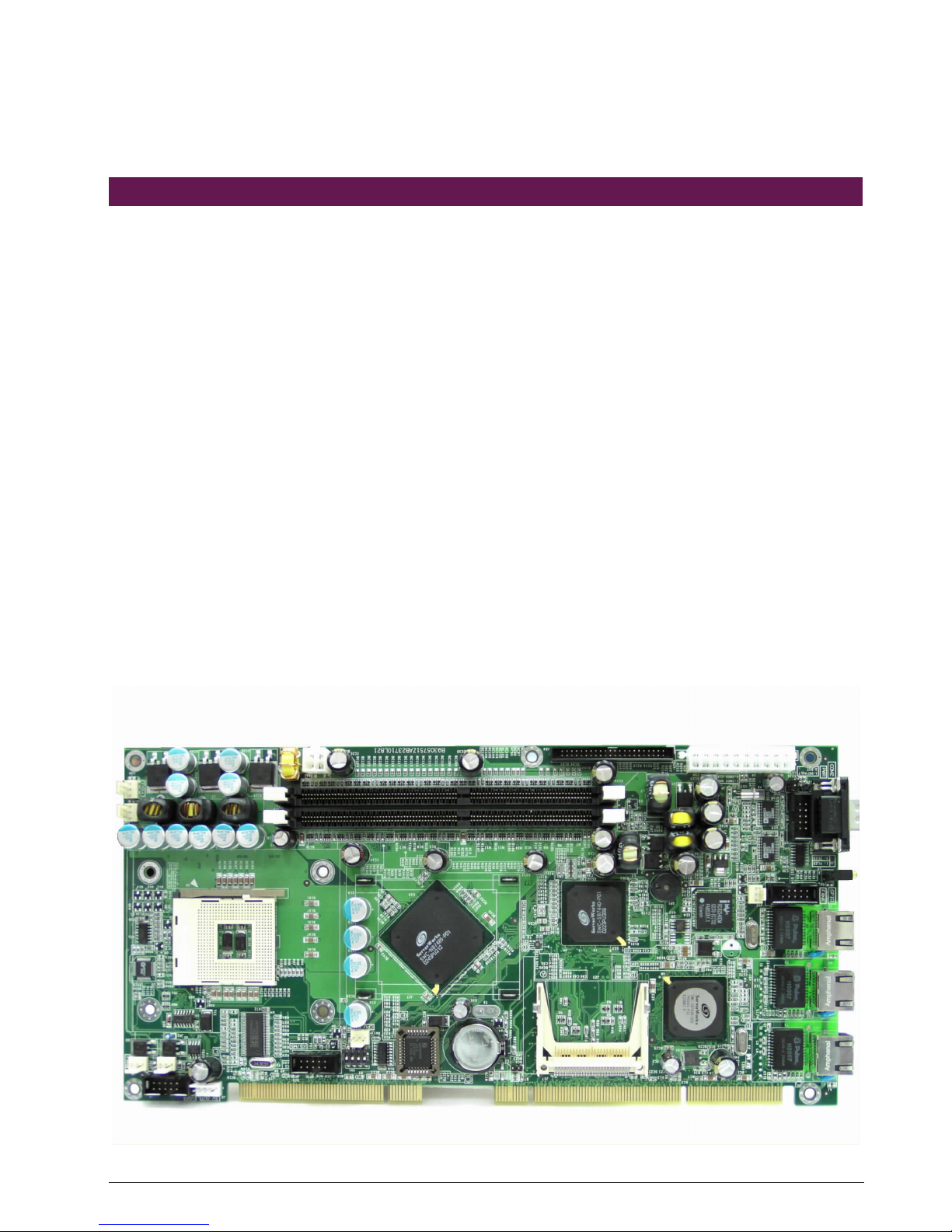
NAR-5050/5070 Series User’s Manual
56
Chapter 3 Operation Guide
3.1 Brief Guide of PPAP-3710L-0200
PPAP-3710L-0200 is a Communication Appliance computing board based on Server Works
CMIC-SL chipset technology. PPAP-3710L-0200 has three on-board LAN ports to serve
communication appliances, such as Firewall, which needs three Ethernet ports to connect
external network (internet), demilitarized zone and internal network. Different I/O management
policies can be applied respectively to individual network to achieve the highest security level.
The target market segment is communication appliance including Virtual Private Network, Load
Balancing, Quality of Service, Intrusion Detection, Virus Detection, Firewall and Voice Over IP.
This PPAP-3710L-0200 system board is utilized with Intel® mPGA Celeron® and Intel® mPGA
Pentium® 4 processors, and 184-pin DIMM up to 4 GB DRAM. The enhanced on-board PCI IDE
interface supports 2 drives up to PIO mode 4 timing and Ultra DMA/100 synchronous mode
feature. The on-board Server Works CSB5 chipset integrates two serial ports driven by two high
performance 16C550-compatible UARTs to provide 16-byte send/receive FIFOs. In addition, the
two Universal Serial Bus ports provide high-speed data communication between peripherals and
PC.
The on-board flash ROM is used to make the BIOS update easier. The high precision Real Time
Clock/Calendar is built to support Y2K for accurate scheduling and storing configuration
information. All of these features make PPAP-3710L-0200 excellent in stand-alone applications.
If any of these items is damaged or missing, please contact your vendor and save all packing
materials for future replacement and maintenance.
Figure 3-1 PPAP-3710L-0200 Board
Page 58
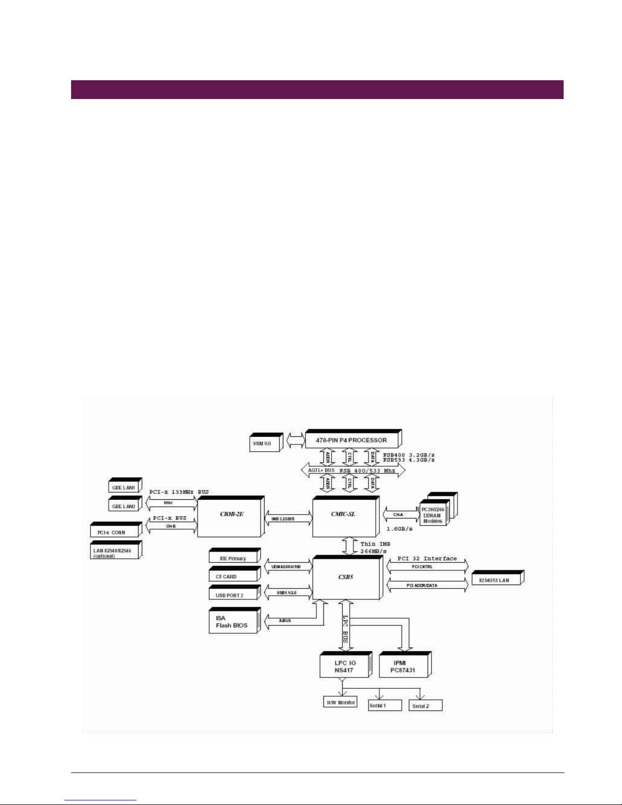
NAR-5050/5070 Series User’s Manual
57
3.2 System Architecture
The following illustration of block diagram illustrated basic design reference of PPAP-3710L0200, a highly integrated system solution. The most up-to-date system architecture of PPAP3710L-0200 includes two main VLSI chips. It contains CMIC-SL and CSB5 to support mPGA
Celeron/Pentium 4 processor, DIMM, PCI bus interface, USB port, SMBus communication, and
Ultra DMA/100 IDE Master. The on-board CSB5 chip supports two UARTs, and hardware
monitoring.
PPAP-3710L-0200 has built-in Socket 478 to support Intel mPGA Celeron/Pentium 4 processor
(400 or 533MHz FSB) for cost-effective and high performance application.
The CMIC-SL provides a completely integrated solution for the system controller and data path
components in a Celeron/Pentium 4 processor system. It provides optimized 64-bit DDRAM
interface with one 184 pin 2.5V DIMM.
The CSB5 provides a highly integrated multifunction for the best industry applications. It
supports 2-channel dedicated Ultra ATA/33/66/100 IDE master interface, Universal Serial Bus
(USB) controllers and two 32-bit PCI bus interfaces.
All detailed operating relations are shown in Fig. 3-2 (PPAP-3710L-0200 System Block
Diagram).
Figure 3-2 PPAP-3710L-0200 Block Diagram
 Loading...