0.5
General Description
η
28.0
V, Vgs = 0V,
V, Vgs = 0V,
V, Vgs = 0V,
F5001
polyfet rf devices
8/1/97
Silicon VDMOS and LDMOS
transistors designed specifically
for broadband RF applications.
Suitable for Military Radios,
PATENTED GOLD METALIZED
SILICON GATE ENHANCEMENT MODE
RF POWER
VDMOSTRANSISTOR
Cellular and Paging Amplifier Base
Stations, Broadcast FM/AM, MRI,
0.5Watts Single Ended
Laser Driver and others.
"Polyfet" process features
TM
Package Style AP
gold metal for greatly extended
lifetime. Low output capacitance
and high F enhance broadband
t
HIGH EFFICIENCY, LINEAR,
HIGH GAIN, LOW NOISE
performance
ABSOLUTE MAXIMUM RATINGS (TC = 25 C)
Total
Device
Dissipation Resistance Temperature Voltage Voltage Voltage
10Watts 13
Junction to
Case Thermal
o
C/W
Maximum
Junction
o
C
200 -65 to 150
Storage
Temperature
o
C
DC Drain
Current
o
0.4 A
C
o
Drain to
Gate
Drain to
Source
VV70 70
Gate to
Source
RF CHARACTERISTICS ( WATTS OUTPUT )
SYMBOL PARAMETER MIN TYP MAX UNITS TEST CONDITIONS
Gps
Common Source Power Gai
8
dB
Idq =
0.1
A,
28.0Vds = V,
F =2000 MHz
30V
VSWR
Drain Efficiency
Load Mismatch Toleranc
35
20:1
%
Relative
Idq =
Idq =
0.1
0.1
A,
A,
ELECTRICAL CHARACTERISTICS (EACH SIDE)
SYMBOL PARAMETER MIN TYP MAX UNITS TEST CONDITIONS
Bvdss
Idss
Igss
Vgs
gM
Rdson
Idsat
Ciss
Crss
Coss
Drain Breakdown Voltag
Zero Bias Drain Curren
Gate Leakage Curren
Gate Bias for Drain Curren
Forward Transconductanc
Saturation Resistanc
Saturation Curren
Common Source Input Capacitanc
Common Source Feedback Capacitanc
Common Source Output Capacitanc
65
0.2
1
71
0.1
4.5
0.6
4
0.4
3
V
mA
uA
V
Mho
Ohm
Amp
pF
pF
pF
POLYFET RF DEVICES
0.01Ids = A,
Vds = V, Vgs = 0V
Vds = 0 V, Vgs = 30V
Ids = A, Vgs = Vds
Vds = 10V, Vgs = 5V
Vgs = 20V, Ids = 1
Vgs = 20V, Vds = 10V
28.0Vds =
28.0Vds =
28.0Vds =
REVISION
28.0Vds = V,
28.0Vds = V,
Vgs = 0V
A
F =2000 MHz
F =2000 MHz
F = 1 MHz
F = 1 MHz
F = 1 MHz
1110 Avenida Acaso, Camarillo, CA 93012 TEL:(805) 484-4210 FAX:(805) 484-3393 EMAIL:Sales@polyfet.com URL:www.polyfet.com

F5001
8/1/97
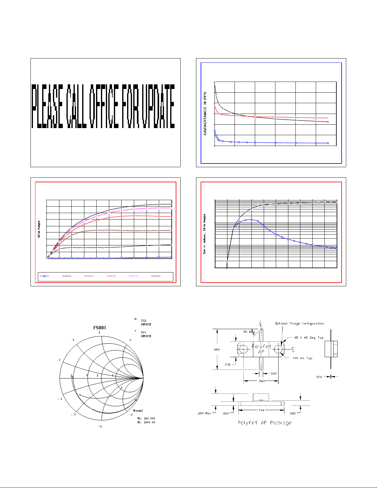
POUT VS PIN GRAPH
IV CURVE ID AND GM VS VGS
F5001 IV CURVE
0.9
0.8
0.7
0.6
0.5
0.4
0.3
0.2
0.1
0
0 2 4 6 8 10 12 14 16 18 20
Vg = 2V Vg = 4V Vg = 6V Vg = 8V Vg = 10V Vg = 12V
Vds in Volts
CAPACITANCE VS VOLTAGE
F5001 CAPACITANCE VS VDS
12
10
8
6
4
2
0
0 5 10 15 20 25 30
1
0.1
0.01
0.001
Coss
Ciss
Crss
VDS IN VOLTS
F5001 DIE GM & ID vs VG
Id
Gm
0 2 4 6 8 10 12 14 16 18 20
Vgs in Volts
S11 AND S22 SMITH CHART PACKAGE DIMENSIONS IN INCHES
POLYFET RF DEVICES
1110 Avenida Acaso, Camarillo, CA 93012 TEL:(805) 484-4210 FAX:(805) 484-3393 EMAIL:Sales@polyfet.com URL:www.polyfet.com
REVISION
 Loading...