查询LY402供应商
polyfet rf devices
General Description
Silicon VDMOS and LDMOS
transistors designed specifically
for broadband RF applications.
Suitable for Militry Radios,
Cellular and Paging Amplifier Base
Stations, Broadcast FM/AM, MRI,
Laser Driver and others.
"Polyfet" process features
low feedback and output capacitances
resulting in high F transistors with high
input impedance and high efficiency.
Dissipation
440
TM
t
ABSOLUTE MAXIMUM RATINGS ( T =
Total
Device
Watts V
Junction to
Case Thermal
Resistance
o
0.38 C/W
Maximum
Temperature
Junction
o
200
SILICON GATE ENHANCEMENT MODE
RF POWER TRANSISTORLDMOS
220.0
Watts
Push - Pull
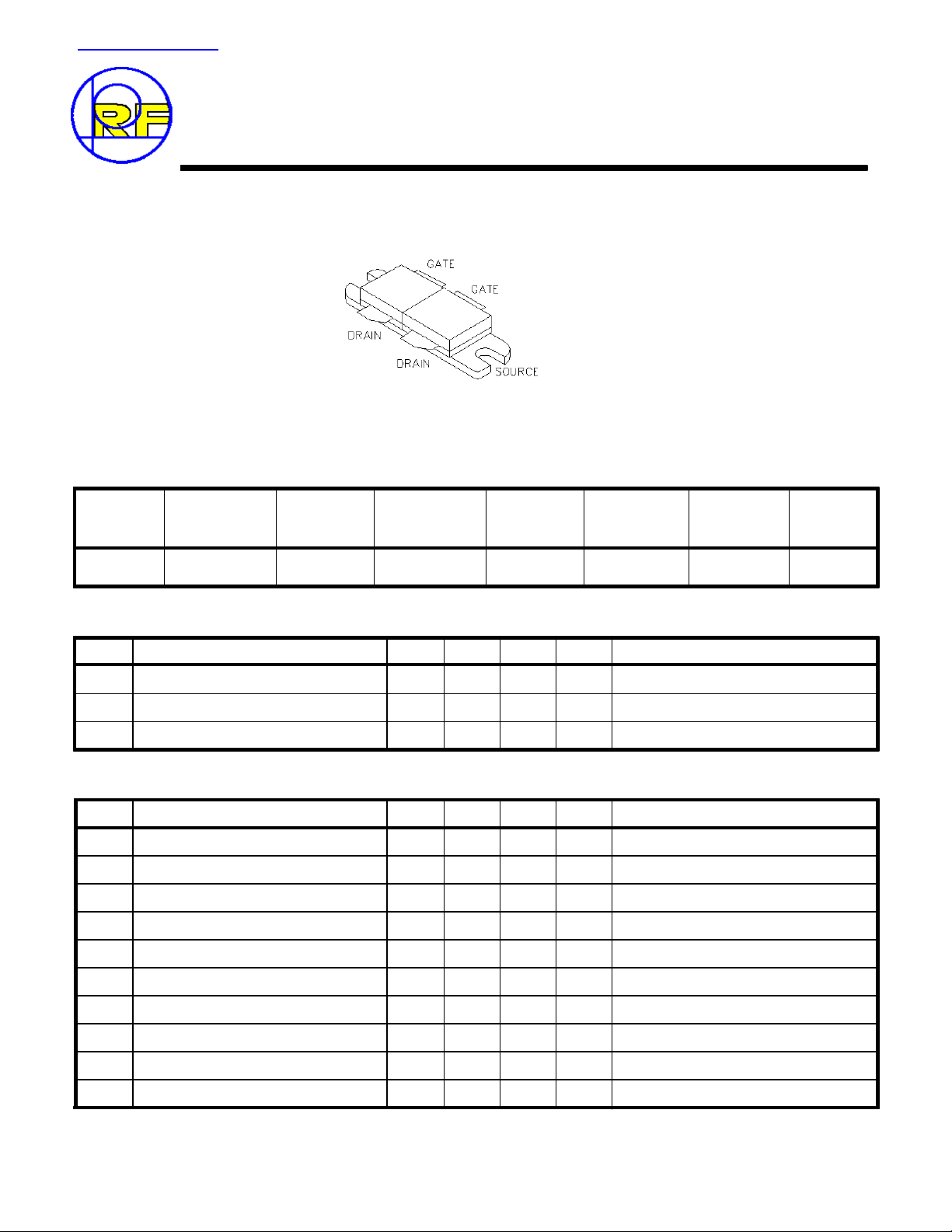
Package Style
HIGH EFFICIENCY, LINEAR
HIGH GAIN, LOW NOISE
o
25 C )
Storage
Temperature
-65 C to 150 C C A V
DC Drain
Current
oo
13.5
Drain to
Gate
Voltage
70 V
Drain to
Source
Voltage
70
LY402
AY
Gate to
Source
Voltage
20
Gps
η
Bvdss
Idss
Igss
Vgs
Idsat
Ciss
Crss
Coss
RF CHARACTERISTICS (
PARAMETERSYMBOL MIN TYP MAX UNITS TEST CONDITIONS
Common Source Power Gain
Drain Efficiency
Load Mismatch ToleranceVSWR
13
60
220.0
WATTS OUTPUT )
dB
20:1 Relative
0.80
Idq = A, Vds = V, F =
Idq =
0.80
%
Idq = 0.80
A, Vds = V, F =
A, Vds = V, F =
28.0
28.0
28.0
ELECTRICAL CHARACTERISTICS ( EACH SIDE )
PARAMETERSYMBOL MIN TYP MAX UNITS TEST CONDITIONS
Drain Breakdown Voltage
Zero Bias Drain Current
Gate Leakage Current
Gate Bias for Drain Current
Forward TransconductancegM Vds = 10V, Vgs = 5V
Saturation Current
Common Source Input Capacitance
Common Source Feedback Capacitance
Common Source Output Capacitance
65
2.0
1
1 7
5.4
0.17
34.00
160.0
8.0
100.0
V
mA
uA
V
Mho
Ohm
Amp
pF
pF
pF
0.50Ids = mA, Vgs = 0V
Vds =
Vds = 0V Vgs = 30V
Vgs = 20V, Ids = Rdson Saturation Resistance
Vgs = 20V, Vds = 10V
Vds =
Vds =
Vds =
28.0
0.30
V, Vgs = 0V
A, Vgs = VdsIds =
16.00
Vgs = 0V, F = 1 MHz28.0
Vgs = 0V, F = 1 MHz28.0
Vgs = 0V, F = 1 MHz28.0
MHz
500
500
MHz
500
MHz
A
POLYFET RF DEVICES
1110 Avenida Acaso, Camarillo, Ca 93012 Tel:(805) 484-4210 FAX: (805) 484-3393 EMAIL:Sales@polyfet.com URL:www.polyfet.com
REVISION 01/17/2002

LY402
ID IN AMPS
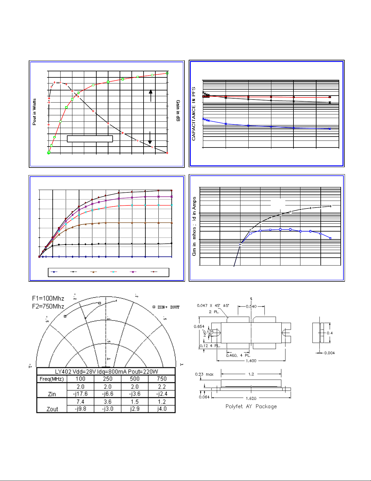
POUT VS PIN GRAPH
LY402 Pin vs Pout F=500Mhz; Vds=28Vdc, Idq=.8A
260
240
220
200
180
160
140
120
100
80
60
40
20
0
0 2 4 6 8 10 12 14 16 18 20
Efficiency @190W = 60%
Pin in Watts
L4 2 DIE IV
35
30
25
20
15
10
5
0
0 2 4 6 8 10 12 14 16 18 20
vg=2v Vg=4v Vg=6v vg=8v vg=10v vg=12v
VDS IN VOLTS
Pout
Gain
CAPACITANCE VS VOLTAGE
18
17
16
15
14
13
12
11
1000
100
10
1
0 5 10 15 20 25 30
L4 2DIE CAPACITANCE
Ciss
Coss
Crss
VDS IN VOLTS
ID & GM VS VGSIV CURVE
100
10
1
0.1
0 2 4 6 8 10 12 14
L4 2 DIE ID, GM vs VG
ID
Vgs in Volts
Zin Zout PACKAGE DIMENSIONS IN INCHES
Tolerance .XX +/-0.01 .XXX +/-.005 inches
01/17/2002
POLYFET RF DEVICES
1110 Avenida Acaso, Camarillo, Ca 93012 Tel:(805) 484-4210 FAX: (805) 484-3393 EMAIL:Sales@polyfet.com URL:www.polyfet.com
REVISION
 Loading...